


 Loading...
AN2383
Application note
A single plate induction cooker with the ST7FLITE09Y0
Introduction
This application note describes an induction cooking design which can be used to evaluate ST components or to get started quickly with your own induction cooking development project.
Induction cooking is not a radically new invention; it has been widely used all around the world. With recent improvements in technology and the consequent reduction of component costs, Induction cooking equipment is now more affordable than ever.
The design provides an opportunity to understand how an induction cooker works and to make an in-depth examination of the various blocks and parts of this type of cooking application such as the driving topology, how the resonant tank works, how the pot gets hot and how to remove it safely from the cooking element.
The design is entirely controlled by a simple ST7FLITE09Y0 8-bit microcontroller, which provides the PWM driving signals, communicates information to the user interface, and drives the fan and relay control to the plate feedback.
September 2009 |
Doc ID 12433 Rev 3 |
1/39 |
www.st.com

Contents |
AN2383 |
|
|
Contents
1 |
Induction heating basics . . . . . . . . . . . . . . . . . . . . . . . . . . . . . . . . . . . . |
. 6 |
|
2 |
Block diagram . . . . . . . . . . . . . . . . . . . . . . . . . . . . . . . . . . . . . . . . . . . . . |
. 7 |
|
3 |
Schematic . . . . . . . . . . . . . . . . . . . . . . . . . . . . . . . . . . . . . . . . . . . . . . . . |
. 8 |
|
|
3.1 |
Mains, DC link voltage and zero voltage switching . . . . . . . . . . . . . . . . . . . |
8 |
|
3.2 |
Isolated power supply . . . . . . . . . . . . . . . . . . . . . . . . . . . . . . . . . . . . . . . . . |
9 |
|
3.3 |
Power stage . . . . . . . . . . . . . . . . . . . . . . . . . . . . . . . . . . . . . . . . . . . . . . . |
10 |
|
3.4 |
Feedbacks . . . . . . . . . . . . . . . . . . . . . . . . . . . . . . . . . . . . . . . . . . . . . . . . |
11 |
|
3.5 |
MCU pin configuration . . . . . . . . . . . . . . . . . . . . . . . . . . . . . . . . . . . . . . . |
12 |
4 |
How the system works . . . . . . . . . . . . . . . . . . . . . . . . . . . . . . . . . . . . . . |
14 |
|
|
4.1 |
Standby (system off) . . . . . . . . . . . . . . . . . . . . . . . . . . . . . . . . . . . . . . . . |
14 |
|
4.2 |
System on . . . . . . . . . . . . . . . . . . . . . . . . . . . . . . . . . . . . . . . . . . . . . . . . |
14 |
|
4.3 |
Safety relay and fan management . . . . . . . . . . . . . . . . . . . . . . . . . . . . . . |
14 |
5 |
Measurements at 50 Hz . . . . . . . . . . . . . . . . . . . . . . . . . . . . . . . . . . . . . . |
15 |
|
|
5.1 |
Standby (system off) . . . . . . . . . . . . . . . . . . . . . . . . . . . . . . . . . . . . . . . . |
15 |
|
5.2 |
Powering the plate (without pot) . . . . . . . . . . . . . . . . . . . . . . . . . . . . . . . . |
16 |
|
5.3 |
Powering the plate (with pot) . . . . . . . . . . . . . . . . . . . . . . . . . . . . . . . . . . |
17 |
|
5.4 |
Working level 1 . . . . . . . . . . . . . . . . . . . . . . . . . . . . . . . . . . . . . . . . . . . . . |
18 |
|
5.5 |
Working level 9 . . . . . . . . . . . . . . . . . . . . . . . . . . . . . . . . . . . . . . . . . . . . . |
19 |
|
5.6 |
Real-time current adjustment . . . . . . . . . . . . . . . . . . . . . . . . . . . . . . . . . . |
19 |
|
5.7 |
Removing the pot . . . . . . . . . . . . . . . . . . . . . . . . . . . . . . . . . . . . . . . . . . . |
20 |
6 |
Measurements at PWM frequency . . . . . . . . . . . . . . . . . . . . . . . . . . . . . |
21 |
|
|
6.1 |
Powering the plate (with pot) . . . . . . . . . . . . . . . . . . . . . . . . . . . . . . . . . . |
21 |
|
6.2 |
Working level 1 . . . . . . . . . . . . . . . . . . . . . . . . . . . . . . . . . . . . . . . . . . . . . |
22 |
|
6.3 |
Working level 9 . . . . . . . . . . . . . . . . . . . . . . . . . . . . . . . . . . . . . . . . . . . . . |
23 |
|
6.4 |
Current waveform at 50 Hz . . . . . . . . . . . . . . . . . . . . . . . . . . . . . . . . . . . . |
24 |
7 |
Alarm management . . . . . . . . . . . . . . . . . . . . . . . . . . . . . . . . . . . . . . . . . |
25 |
|
2/39 |
Doc ID 12433 Rev 3 |

AN2383 Contents
8 |
User interface . . . . . . . . . . . . . . . . . . . . . . . . . . . . . . . . . . . . . . . . . . . . . |
26 |
|
|
8.1 |
Keyboard schematic . . . . . . . . . . . . . . . . . . . . . . . . . . . . . . . . . . . . . . . . . |
26 |
|
8.2 |
Display schematic . . . . . . . . . . . . . . . . . . . . . . . . . . . . . . . . . . . . . . . . . . |
27 |
9 |
Software management . . . . . . . . . . . . . . . . . . . . . . . . . . . . . . . . . . . . . . |
28 |
|
10 |
Thermal conditions . . . . . . . . . . . . . . . . . . . . . . . . . . . . . . . . . . . . . . . . . |
30 |
|
11 |
Bill of material . . . . . . . . . . . . . . . . . . . . . . . . . . . . . . . . . . . . . . . . . . . . . |
31 |
|
12 |
Demonstration board . . . . . . . . . . . . . . . . . . . . . . . . . . . . . . . . . . . . . . . |
34 |
|
13 |
References and related materials . . . . . . . . . . . . . . . . . . . . . . . . . . . . . |
37 |
|
14 |
Revision history . . . . . . . . . . . . . . . . . . . . . . . . . . . . . . . . . . . . . . . . . . . |
38 |
|
Doc ID 12433 Rev 3 |
3/39 |

List of tables |
AN2383 |
|
|
List of tables
Table 1. Bill of material (part 1 of 3) . . . . . . . . . . . . . . . . . . . . . . . . . . . . . . . . . . . . . . . . . . . . . . . . . 31 Table 2. Bill of material (part 2 of 3) . . . . . . . . . . . . . . . . . . . . . . . . . . . . . . . . . . . . . . . . . . . . . . . . . 32 Table 3. Bill of material (part 3 of 3) . . . . . . . . . . . . . . . . . . . . . . . . . . . . . . . . . . . . . . . . . . . . . . . . . 33 Table 4. Document revision history . . . . . . . . . . . . . . . . . . . . . . . . . . . . . . . . . . . . . . . . . . . . . . . . . 38
4/39 |
Doc ID 12433 Rev 3 |

AN2383 |
List of figures |
|
|
List of figures
Figure 1. Induction cooking design block diagram . . . . . . . . . . . . . . . . . . . . . . . . . . . . . . . . . . . . . . . . 7 Figure 2. Mains and +325 volt DC link . . . . . . . . . . . . . . . . . . . . . . . . . . . . . . . . . . . . . . . . . . . . . . . . 8 Figure 3. Isolated power supply, 5 and 15 volt . . . . . . . . . . . . . . . . . . . . . . . . . . . . . . . . . . . . . . . . . . 9 Figure 4. L6384 IGBT driver and power stage . . . . . . . . . . . . . . . . . . . . . . . . . . . . . . . . . . . . . . . . . . 10 Figure 5. Current peak, current phase and alarm . . . . . . . . . . . . . . . . . . . . . . . . . . . . . . . . . . . . . . . 11 Figure 6. MCU pin configuration . . . . . . . . . . . . . . . . . . . . . . . . . . . . . . . . . . . . . . . . . . . . . . . . . . . . 12 Figure 7. System in standby mode . . . . . . . . . . . . . . . . . . . . . . . . . . . . . . . . . . . . . . . . . . . . . . . . . . 15 Figure 8. Plate power-on (without pot on the plate) . . . . . . . . . . . . . . . . . . . . . . . . . . . . . . . . . . . . . . 16 Figure 9. Plate power-on (with pot on the plate) . . . . . . . . . . . . . . . . . . . . . . . . . . . . . . . . . . . . . . . . 17 Figure 10. System working at level 1 . . . . . . . . . . . . . . . . . . . . . . . . . . . . . . . . . . . . . . . . . . . . . . . . . . 18 Figure 11. System working at level 9 . . . . . . . . . . . . . . . . . . . . . . . . . . . . . . . . . . . . . . . . . . . . . . . . . . 19 Figure 12. Plate power-on (with pot on the plate) . . . . . . . . . . . . . . . . . . . . . . . . . . . . . . . . . . . . . . . . 21 Figure 13. System working at level 1 . . . . . . . . . . . . . . . . . . . . . . . . . . . . . . . . . . . . . . . . . . . . . . . . . . 22 Figure 14. System working at level 9 . . . . . . . . . . . . . . . . . . . . . . . . . . . . . . . . . . . . . . . . . . . . . . . . . . 23 Figure 15. Current waveform at 50 Hz . . . . . . . . . . . . . . . . . . . . . . . . . . . . . . . . . . . . . . . . . . . . . . . . . 24 Figure 16. The analog keyboard . . . . . . . . . . . . . . . . . . . . . . . . . . . . . . . . . . . . . . . . . . . . . . . . . . . . . 26 Figure 17. Display circuitry. . . . . . . . . . . . . . . . . . . . . . . . . . . . . . . . . . . . . . . . . . . . . . . . . . . . . . . . . . 27 Figure 18. The six most important software events . . . . . . . . . . . . . . . . . . . . . . . . . . . . . . . . . . . . . . . 28 Figure 19. Demonstration board photo (no cooking plate connected) . . . . . . . . . . . . . . . . . . . . . . . . . 34 Figure 20. User interface . . . . . . . . . . . . . . . . . . . . . . . . . . . . . . . . . . . . . . . . . . . . . . . . . . . . . . . . . . . 35 Figure 21. Resonant capacitors (in blue) . . . . . . . . . . . . . . . . . . . . . . . . . . . . . . . . . . . . . . . . . . . . . . . 35 Figure 22. Reverse angle. . . . . . . . . . . . . . . . . . . . . . . . . . . . . . . . . . . . . . . . . . . . . . . . . . . . . . . . . . . 36
Doc ID 12433 Rev 3 |
5/39 |

Induction heating basics |
AN2383 |
|
|
1 Induction heating basics
Put simply, an induction cooking element (what on a gas stove would be called a "burner") is a special kind of transformer. When a good-sized piece of magnetically conducting material such as, for example, a cast-iron frying pan, is placed in the magnetic field created by the cooking element, the field transfers ("induces") energy into the metal. That transferred energy causes the metal - the cooking vessel - to become hot.
By controlling the intensity of the magnetic field, we can control the amount of heat being generated in the cooking vessel and we can change that amount instantaneously.
Induction cooking has several advantages over traditional methods of cooking:
●Speed: conductive heat transfer to the food is very direct because the cookware is heated uniformly and from within. Induction cooking is even faster than gas cooking
●Safety: there are no open flames. This reduces the chances of fire and the cold stove top is also more child safe
●Efficiency: around 90%. Heat is generated directly in the pot, while for electric and gas the efficiency is around 65% and 55% respectively due to heat transfer loss.
Induction cooking functions based on the principle of the series L-C resonant circuit, where the inductance L is the cooking element itself.
By changing the switching frequency of the high voltage half-bridge driver, the alternating current flowing through the cooking element changes its value. The intensity of the magnetic field and therefore the heating energy can be controlled this way.
6/39 |
Doc ID 12433 Rev 3 |
AN2383 |
Block diagram |
|
|
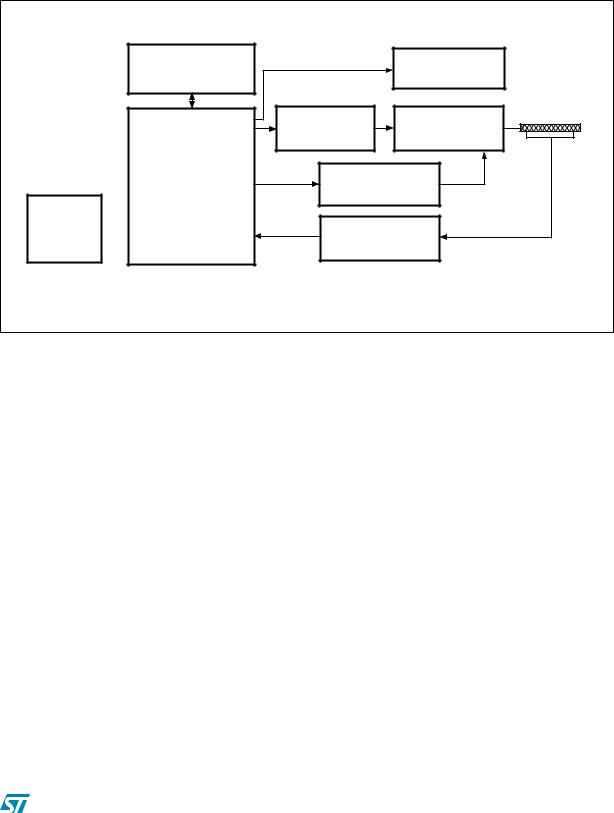
2 Block diagram
Figure 1. Induction cooking design block diagram
|
USER INTERFACE |
FAN |
|
|
|
PLATE |
|
|
DRIVER |
2x IGBTs |
|
|
MCU |
|
|
|
ST7LITE |
RELAY |
|
|
|
||
POWER |
|
|
|
SUPPLY |
PLATE FEEDBACK |
||
5 / 15V |
|||
|
|
||
|
|
AI12605 |
|
The induction cooking design consists of a small number of simple blocks.
The isolated power supply is obtained directly from the mains, 220 V AC 50 Hz. 15 volts are used to supply the IGBT driver, fan, relay and feedback circuitry, while 5 volts are needed to supply the rest of the ICs, including the MCU.
The ST7FLITE09Y0 microcontroller controls the whole process and communicates with the user interface (buttons and display), drives the fan and the relay, receives feedback from the cooking element (referred to in this document as “plate” for simplicity) and generates the PWM signal to drive the IGBTs.
Doc ID 12433 Rev 3 |
7/39 |
Schematic |
AN2383 |
|
|
3 Schematic
Although the schematic is not very complex, this section presents the different parts as separate topics:
●Mains, DC link and zero voltage switching
●Isolated power supply
●Power stage
●Feedbacks
●MCU pin configuration
The user interface schematic is not presented in this section. It is discussed and analyzed in
Section 8.
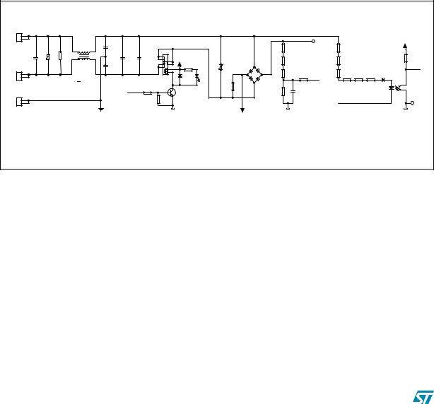
3.1Mains, DC link voltage and zero voltage switching
Figure 2. Mains and +325 volt DC link
FST1 |
|
|
|
|
|
|
|
|
|
|
|
|
|
|
|
|
|
|
|
|
NEUTRAL |
|
|
|
|
ACN |
|
|
|
|
|
|
|
|
|
|
+325V |
|
|
|
|
1 |
|
|
|
|
|
|
|
|
|
|
|
|
|
|
|
|
+5V |
|||
2 |
|
|
|
C 2 |
|
|
2 |
|
|
|
|
|
|
|
|
|
TP14 |
|
|
|
|
1 |
4 |
|
|
|
|
|
|
|
|
|
|
R6 |
R11 |
|
|
|
|||
C1 |
RV1 R1 |
|
|
|
|
|
|
|
|
|
|
|
|
|
|
|||||
|
|
|
|
|
|
|
|
|
|
|
|
|
|
|
||||||
1µF |
470K 2 |
3 |
3n3Y1 |
C4 |
C5 |
7 |
3 |
|
+15V |
|
|
|
|
|
220K |
4K3 |
50Hz |
R16 |
||
275V X2 |
C 3 |
1µF |
1µF |
4 |
6 |
R4 |
RV2 |
|
|
R7 |
R12 |
2K2 |
||||||||
FST2 |
460V 1W |
L1 |
|
275VX2 275VX2 |
|
|
~ |
|
220K |
4K3 |
|
|
|
|||||||
|
|
|
|
|
|
1 |
|
8K2 |
275V |
|
|
|
|
|||||||
LI N E 1 |
|
|
|
3n3Y1 AC L |
|
5 |
|
|
+ |
|
R10 |
|
R14 R15 R17 D13 |
|
||||||
|
|
|
|
|
8 |
D1 |
|
DL1 |
- |
R8 |
R13 |
|
||||||||
2 |
TDKFT2510H |
|
|
RL1 |
12V |
|
|
|
~ D2 270K |
4K7 |
4K3 |
4K3 4K3 4K3 1N4007 |
|
|||||||
|
|
|
1N4007 |
|
R5 |
|
|
1 |
4 |
|||||||||||
|
|
|
LED |
|
VLINK |
|
||||||||||||||
FS T3 |
|
|
|
RELAY |
16A250VAC |
Q3 |
|
470K |
25A |
R9 |
C6 |
|
|
3 |
||||||
EARTH |
|
|
|
|
|
|
|
|
|
|
|
|||||||||
|
|
|
|
R 2 |
R3 |
|
|
BC337 |
|
|
1W |
|
22nF |
|
ACL |
2 ISO2 |
||||
1 |
|
|
|
|
|
|
|
|
|
|
8K2 |
|
|
TP17 |
||||||
|
|
|
|
|
4K7 |
10K |
|
|
|
|
|
|
|
|
|
|
|
|
|
|
2 |
|
|
|
|
|
|
|
|
|
|
|
|
|
|
|
|
|
PC817 |
||
|
|
|
|
|
|
|
|
|
|
|
|
|
|
|
|
|
|
|||
|
|
|
|
|
|
|
|
|
|
|
|
|
|
|
|
|
|
|
AI12612 |
|
The mains is filtered and is not applied directly to the power diode bridge: for safety reasons, it goes through a relay. This means that the DC link voltage is not applied to the IGBT while the system is off.
The 14 V DC relay is driven by the MCU through a classic NPN transistor. An LED is also present.
When the system is on - and the AC line is applied to the power diode bridge - the IGBTs are supplied with +325 V. The resistive divider sends an image of the DC link voltage to the MCU (label VLINK). The last part of the schematic is an isolated zero voltage switching (ZVS): a square waveform at 50 Hz synchronized with the mains (label 50 Hz).
8/39 |
Doc ID 12433 Rev 3 |

AN2383 |
Schematic |
|
|
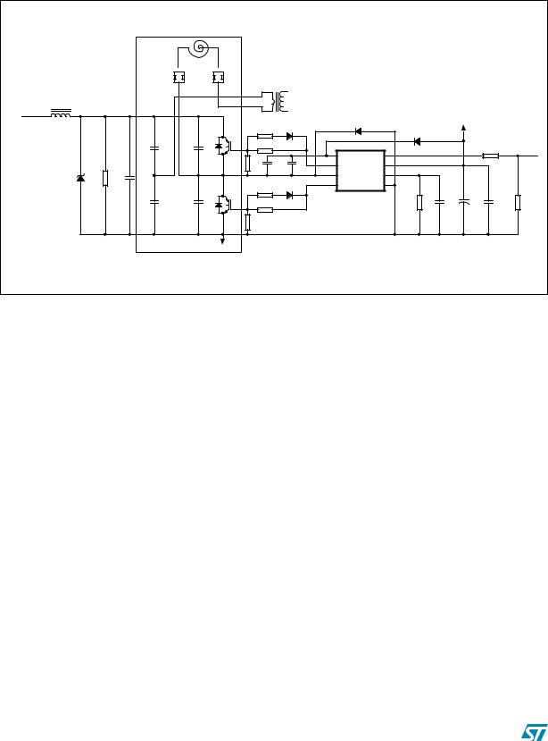
3.2Isolated power supply
Figure 3. Isolated power supply, 5 and 15 volt
|
|
|
L3 |
|
|
|
|
|
|
T1 |
|
D10 |
+15V |
|
|
|
|
|
|
|
|
330µH |
|
|
|
|
|
|
|
|
|
|
|
|
|
||
|
|
|
|
|
|
|
|
|
TRONIC |
STPS2H100 |
|
|
|
|
|
|||
ACL |
|
|
|
|
|
|
|
|
|
|
|
|
|
|
||||
|
|
|
|
|
|
|
|
|
3 |
8 |
|
|
TP 15 |
|
|
|
||
|
|
|
|
|
|
|
|
|
|
|
|
|
|
|
|
|
||
|
|
|
|
|
D15 |
|
|
|
|
|
|
R3 0 |
+ C26 |
|
|
|
|
|
|
|
|
|
|
PKC-136 |
|
|
|
|
|
n.c. |
33 0µF |
|
|
|
|||
|
|
|
|
|
|
|
|
|
|
|
|
|
|
|||||
|
|
|
|
|
|
|
|
|
|
4 |
5 |
|
|
35V |
|
|
|
|
|
|
|
|
8 |
7 |
6 |
5 |
|
|
2 |
|
|
|
|
|
U6 |
|
+5V |
|
|
|
|
Drain4 |
Drain3 |
Drain2 |
Drain1 |
|
R29 |
D14 |
|
|
+15V |
+15V |
|
|||
|
~ |
|
|
|
|
|
L7805CV |
|
||||||||||
|
|
|
4 |
10 |
BAR46 |
|
|
|
|
|
TP 16 |
|||||||
|
|
|
|
|
|
|
|
|
|
|
1 VIN |
VOUT 3 |
||||||
– |
+ |
|
|
Source2 |
Source1 |
|
VDD |
|
|
1 |
|
|
|
|
||||
|
|
|
|
|
|
R38 |
R47 |
|
|
|||||||||
|
|
|
|
|
|
3 |
|
C4 1 |
|
|
GND |
|
||||||
|
|
|
|
|
|
|
1K |
24K |
|
|
|
|||||||
|
~ |
|
|
|
FB |
|
2n2Y |
|
|
2 |
|
|
||||||
|
|
|
|
|
|
|
|
|
|
|
|
|||||||
|
|
|
|
|
|
|
|
|
|
|
|
|
|
|||||
|
D16 |
C22 + |
C23 + |
|
|
|
|
|
|
|
|
|
|
|
|
|
||
|
|
|
|
|
|
|
|
|
|
|
|
|
|
|
|
|||
ACN |
1,5A |
10µF |
10µF |
2 |
1 |
U4 |
|
|
|
|
|
|
|
|
C27 |
C28 |
|
|
|
400V |
400V |
|
|
VIPer22A |
|
3 |
4 |
R39 |
|
|
330nF |
100 nF |
|
||||
|
|
|
|
|
|
|
|
|
|
|||||||||
|
|
|
|
|
|
|
|
|
|
1 |
2 |
1K |
|
|
|
|
|
|
|
|
|
|
|
|
|
|
|
|
C24 |
R46 |
|
|
|
|
|
||
|
|
|
|
|
|
|
|
|
|
ISO1 |
|
|
|
|
|
|||
|
|
|
|
|
|
|
|
|
|
100nF 4K7 |
|
|
|
|
|
|||
|
|
|
|
|
|
|
|
|
|
815 |
|
|
+ |
C38 |
C29 |
+ |
||
|
|
|
|
|
|
|
|
|
+ C25 |
C40 |
U5 |
|
|
|||||
|
|
|
|
|
|
|
|
|
|
|
|
100µF |
10µF |
|
||||
|
|
|
|
|
|
|
|
|
10µF |
22nF |
TL431I |
|
|
|
|
|||
|
|
|
|
|
|
|
|
|
|
R48 |
|
35V |
16V |
|
||||
|
|
|
|
|
|
|
|
|
35V |
|
|
|
|
|
||||
|
|
|
|
|
|
|
|
|
|
|
|
|
4K7 |
|
|
|
|
|
|
|
|
|
|
|
F |
|
|
|
|
|
|
|
|
|
|
|
|
|
|
|
|
|
|
|
|
|
|
|
|
|
|
|
|
|
AI12611 |
|
An isolated power supply is connected immediately after the mains filtering, without passing through the safety relay. A VIPer22A and a simple voltage regulator provide 15 and 5 volts respectively. The power supply ground is isolated from the system ground.
Doc ID 12433 Rev 3 |
9/39 |
Schematic |
AN2383 |
|
|
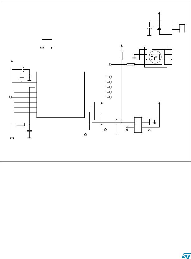
3.3Power stage
Figure 4. L6384 IGBT driver and power stage
|
|
PLATE |
|
|
|
|
|
|
|
|
|
|
|
|
|
|
|
|
|
|
FST4 |
FST5 |
|
|
T2 |
|
|
|
|
|
|
|
|
|
|
|
|
|
|
|
|
TDKCT034 |
|
|
|
|
|
|
|
|
|
|
||||
|
|
SCREW |
SCREW |
|
1:20 |
0 |
|
|
|
|
|
|
|
|
|
|
||
|
|
1 |
|
|
1 |
|
|
|
|
|
|
|
|
|
|
|||
|
|
|
|
4 |
|
1 |
|
|
|
|
|
|
|
|
|
|
||
L2 |
|
|
|
|
|
|
|
|
|
|
|
|
|
|
|
|
||
|
|
|
|
|
|
|
|
|
|
|
|
|
|
|
|
|
|
|
80µH |
|
|
|
|
|
3 |
|
2 |
|
|
|
|
|
|
|
|
|
|
+3 25V |
|
|
|
|
|
|
|
D17 |
|
|
|
+15V |
|
|
|
|||
|
|
|
|
STGY40NC60VD |
|
|
|
|
|
|
|
|
|
|
|
|||
|
|
|
|
|
R22 |
|
D8 |
|
|
|
|
|
|
|
|
|
||
|
|
|
|
|
|
|
STTH102 |
D18 |
|
|
|
|
|
|
||||
|
|
|
|
Q1 |
11R |
|
STTH102 |
|
|
|
|
|
|
|
|
|
||
|
|
|
|
|
|
|
|
|
|
ST TH102 |
|
|
|
|
|
|
||
|
|
C11 |
C13 |
|
R2147R |
|
|
|
|
|
|
R27 |
PWM0 |
|||||
|
|
|
|
|
|
8 |
|
|
1 |
|
|
1K |
|
|||||
|
|
680n |
33nF |
|
|
|
|
VBOOT |
IN |
|
|
|
|
|
|
|||
|
|
800V |
800V |
R20 |
C36 |
C15 |
7 |
2 |
|
|
|
|
|
|
||||
|
|
|
|
HVG |
VCC |
|
|
|
|
|
|
|||||||
|
|
|
|
10K |
47nF |
1µF |
|
3 |
|
|
|
|
|
|
||||
TR1 |
R19 |
C10 |
|
STGY40NC60VD |
|
R25 |
D9 |
6 VOUT DT/SD |
|
|
|
|
|
|
||||
15KE. |
470K |
3µF |
|
|
5 LVG |
GND |
4 |
|
|
|
|
|
|
|||||
|
1W |
400V |
|
Q2 |
11R |
STTH102 |
|
|
|
R26 |
C16 |
|
C17 |
|
|
|
||
|
|
|
|
|
|
|
U2 |
+ |
C37 |
|
R28 |
|||||||
|
|
C12 |
|
|
|
|
|
|
|
|
||||||||
|
|
680nF |
|
|
|
|
|
|
L6384 |
220K |
2n2 |
|
10µF |
47nF |
4K7 |
|||
|
|
800V |
C14 |
|
R24 |
|
|
|
|
|
|
|
|
35V |
|
|
|
|
|
|
|
33nF |
R23 |
|
|
|
|
|
|
|
|
|
|
|
|
||
|
|
|
800V |
47R |
|
|
|
|
|
|
|
|
|
|
|
|
||
|
|
|
10K |
|
|
|
|
|
|
|
|
|
|
|
|
|||
|
|
|
|
|
|
|
|
|
|
|
|
|
|
|
|
|
||
|
|
|
|
|
|
|
|
|
|
|
|
|
|
|
|
|
AI12613 |
|
The +325 V DC link voltage is applied through a filter to the upper-side IGBT only when the safety relay is closed and the system is on. Components inside the dotted rectangle are the core part of the power stage: the L-C resonant tank is obtained by the plate (represented in the schematic by a spiral) and the capacitors on the left side. The resonant capacitor has been divided in two identical capacitors, so that the amount of current flowing through each capacitor is reduced by half, while the voltage to the capacitors remains the same.
A current transformer has been placed in series with the plate in order to provide plate feedback information to the MCU.
The IGBTs are driven by high frequency complementary square waves with 50% duty cycle.
The PWM0 signal applied to the driver input pin is generated directly by the MCU. The frequency varies in a range between 19 kHz and 60 kHz.
For more information regarding the dead time, charging pump capacitor and driving topology, please refer to the L6384 datasheet.
10/39 |
Doc ID 12433 Rev 3 |
AN2383 |
Schematic |
|
|
3.4Feedbacks
Figure 5. Current peak, current phase and alarm
|
|
|
|
|
|
|
|
|
|
|
+15V |
|
+15V |
|
|||
T2 |
|
|
D4 |
|
|
|
|
|
|
R41 |
|
C31 |
TP19 |
|
|
R37 |
|
|
|
STTH102 |
|
|
|
|
|
100K |
+8 |
|
|||||||
|
|
|
|
|
|
|
100nF |
5 |
|
||||||||
TDK_CT03 4 |
|
|
|
|
|
|
|
|
7 |
10K TMP2 |
|||||||
1:200 |
1 |
R18 |
|
D6 |
STTH102 |
|
|
|
|
|
|
|
6 |
– |
4 |
|
|
4 |
100R |
|
|
|
R31 |
|
|
NTC2 |
|
|
R40 |
R44 U3B LM 258 |
|||||
|
|
|
|
D7 |
|
33R |
|
|
PT1000 |
|
62K |
1M |
|
|
|
||
|
|
|
|
|
|
|
|
|
|
|
|
|
|||||
3 |
2 |
|
D5 |
STTH102 |
1W |
|
|
|
|
|
|
|
|
Temperature control |
|||
|
|
|
|
|
|
|
|
|
|
|
|||||||
|
|
|
STTH102 |
|
|
|
|
|
|
|
|
|
|
|
for plate with |
||
|
|
|
|
|
|
|
|
|
|
|
|
+15V |
|
|
PT1000 sensors |
||
|
|
|
|
|
|
|
|
|
|
|
|
+15V |
|
||||
|
|
|
|
|
+5V |
|
R32 |
|
|
TP20 |
|
TP18 |
|
C21 |
|
||
|
|
|
|
|
|
|
|
|
|
100nF |
|
||||||
|
|
|
|
NTC4 |
|
R68 |
2K7 |
|
|
R35 |
|
PT1 |
|
|
8 |
R45 |
|
|
|
|
|
|
1K |
TMP1 |
|
I-CTRL |
2K2 |
|
|
3 |
1 |
12KALARM |
|||
|
|
|
|
47K |
|
|
|
|
50K |
|
+ |
||||||
|
|
|
|
R69 |
|
C44 |
|
|
|
|
|
|
|
2 |
– |
U3A |
|
|
|
|
|
|
R33 |
C18 |
R34 |
R36 |
C19 |
|
|
4 |
|
||||
|
|
|
|
100K |
|
10nF |
n.c. |
22nF |
1K8 |
4K7 |
22nF |
|
|
|
LM 258 |
|
|
|
|
|
|
|
|
|
|
|
|
|
|
||||||
|
|
|
|
|
|
|
|
|
|
|
|
|
C20 |
TH1 |
Alarm management |
||
|
|
|
|
|
|
|
|
|
|
|
|
|
22nF 110 |
|
|
||
|
|
|
|
|
|
|
|
|
|
|
|
|
|
|
|
|
AI12610 |
Feedback signals are output by the current transformer placed in series with the plate, and temperature sensors.
The most important feedback is the current signal (label I-CTRL), which sends the MCU an image of the current flowing through the plate. This signal is used to monitor the current and set it in accordance with the selected working level.
In addition, the signal coming from the current transformer is sent to an operational amplifier. If for any reason the current increases too much, exceeding the alarm threshold set by the potentiometer, the MCU immediately takes action to prevent damage to the power stage.
A NTC has been glued to the heatsink between the IGBTs. The signal is sent to the MCU to monitor the heatsink temperature and drive the fan accordingly. In the same way, a PT1000 is placed in the middle of the plate to monitor the plate temperature. The signal is amplified and sent to the MCU for processing.
Waveforms and a description of how these signals interact with the MCU are given in
Section 5: Measurements at 50 Hz.
Doc ID 12433 Rev 3 |
11/39 |
Schematic |
AN2383 |
|
|
3.5MCU pin configuration
Figure 6. MCU pin configuration
|
|
+15V |
|
|
|
|
|
J8 |
|
C3 0 |
|
|
FAN |
|
+ |
D3 |
1 |
||
100µF |
||||
|
1N4007 |
2 |
||
35 V |
|
|
|
+5V C35 220µF 16V
+
C8
100nF
TP1 I-CTRL TP2 KEYS TP3
 TMP1 TP4
 TMP2 TP5
 VLINK
VLINK
R51
1M
+5V |
Q5 |
STS5NF60L |
|
|
|
|
1 |
8 |
|
|
|
R50 |
2 |
7 |
|
|
|
3 |
6 |
|
|
ExternalI nterrupt request: |
TP12 |
10K |
||
|
|
|
|
||
|
|
|
4 |
5 |
|
|
PA0 -16- ei0 - ALARM |
|
|
||
U1 |
|
R49 |
|
|
|
PA7 - 9 - ei1 - 50Hz |
|
|
|
||
ST 7F LITE09 |
|
|
|
||
|
100 |
|
|
1 |
|
|
|
|
|
16 |
ei0 ALARM |
|
Fan control |
|||||||
|
VSS |
|
PA0 (HS)/LTIC |
|
TP6 |
|||||||||||
2 |
|
15 |
|
|
DATA |
|||||||||||
|
VDD |
|
PA1(HS) |
|
|
|
TP7 |
|||||||||
|
|
|
|
|
PWM0 |
|
||||||||||
3 |
|
|
PA 2(HS)/ATPWMO |
14 |
|
|
|
TP8 |
||||||||
|
RESET |
|
||||||||||||||
|
|
|
|
|
|
|
|
|
|
|
||||||
4 |
|
13 |
|
|
SCLK |
|
||||||||||
|
|
SS/AIN0/PB0 |
PA3(HS) |
|
|
|
TP9 |
|||||||||
|
|
|
||||||||||||||
|
|
|
|
/LE |
|
|||||||||||
5 |
|
SCK/AIN1/PB1 |
PA 4(HS) |
12 |
|
|
|
TP10 |
||||||||
|
|
|
|
+5V |
||||||||||||
6 |
|
MISO/AIN 2/PB 2 |
PA5(HS)/ICCDATA |
11 |
|
|
+5V |
|||||||||
|
|
|
|
|
|
|
|
|
|
|||||||
7 |
|
MOSI/AIN3/PB3 |
PA6/MCO/ICCCLK |
10 |
|
|
|
|
|
|
|
|
||||
8 |
|
CLKIN/AI N4/PB4 |
PA7 |
9 |
|
|
|
|
|
|
R52 |
|
||||
|
|
|
|
|||||||||||||
|
|
|
|
|
|
|
|
|
|
|
|
|
|
10K |
|
|
|
ei1 |
|
|
2 |
1 |
|
|
|
4 |
3 |
|
|
|
|
|
6 |
5 |
|
|
50Hz |
|
8 |
7 |
C9 |
|
TP13 |
10 |
9 |
|
|
RELAY |
|
|
||
10 nF |
TP11 |
|
|
J7 |
|
|
|
|
|
||
|
|
|
|
|
Reset Pin Hints:
R51 is mandatory if residual voltage is still on Reset Pin.
R52 is not mandatory, its functionality has to be checked dur ing tests.
CON10A
I CC Programmer
AI12608
The ST7FLITE09Y0 microcontroller controls the whole induction cooking system. It can be in-circuit programmed (ICP) via a standard 10-pin connector.
Starting from the left, going clockwise, the first input is the VLINK. It comes from the power diode bridge and is an image of the DC link voltage applied to the upper side IGBT. Read as analog input, this signal is used by the MCU to detect when a pot is placed on the plate or when it has been removed.
TMP1 and TMP2 provide the MCU with the temperature information coming from the heatsink and plate, respectively.
KEYS is an analog input read by the internal A/D converter of the MCU, and is connected to the keyboard in the user interface. The keyboard features 3 buttons. In order to save MCU pins, a smart schematic has been adopted, so that just one input pin is needed to read all the keys.
The I-CTRL feedback is processed as analog input. It is an image of the current flowing through the plate.
12/39 |
Doc ID 12433 Rev 3 |
Loading...