


L6219
Table of contents
 Loading...
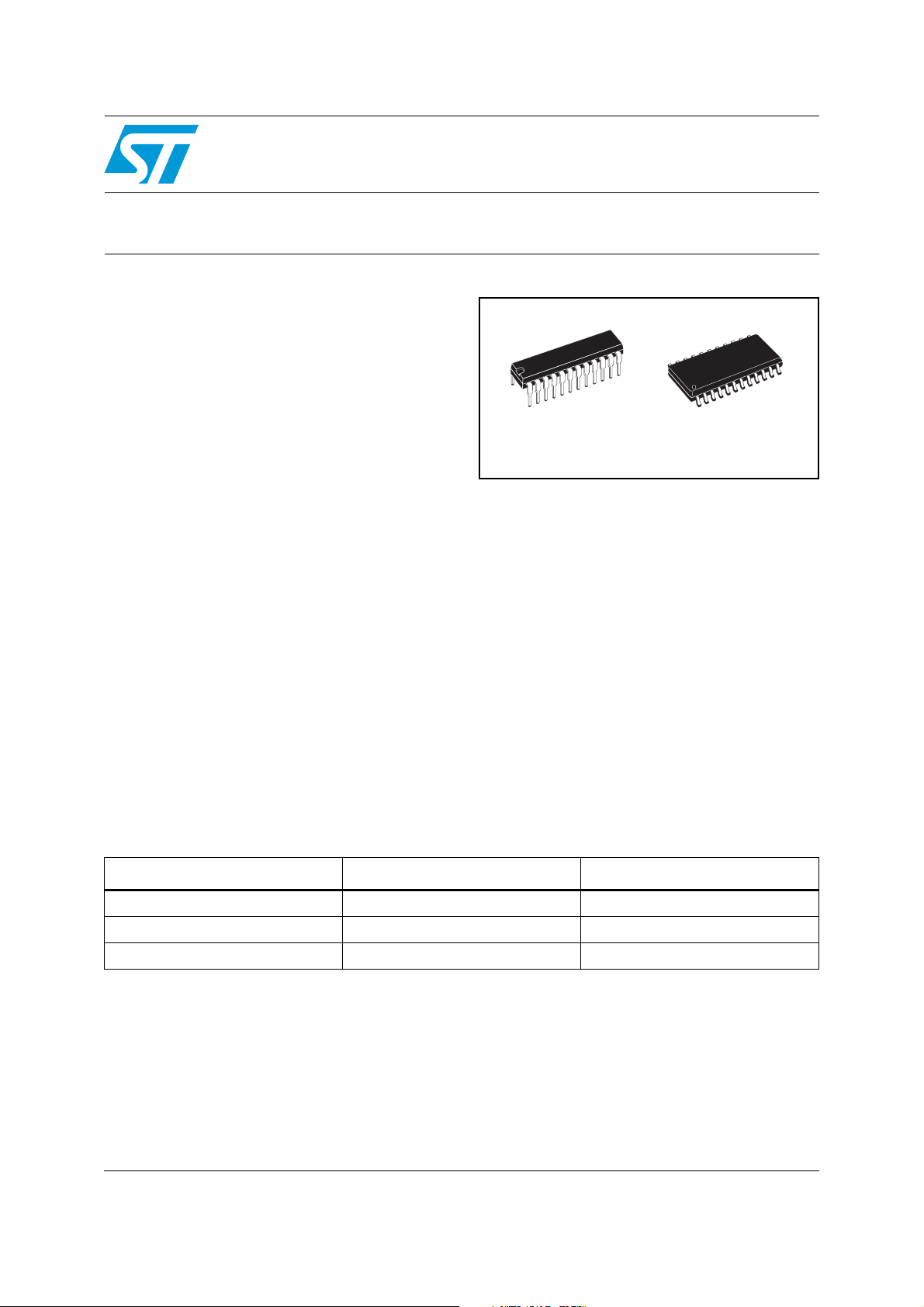
September 2008 Rev 13 1/16
1
L6219
Stepper motor driver
Features
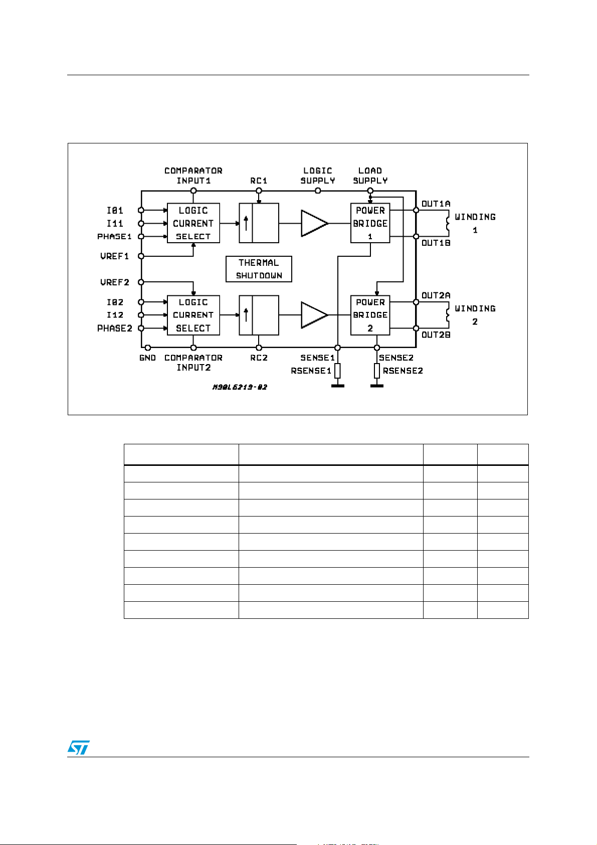
■ Able to drive both windings of bipolar stepper
motor
■ Output current up to 750 mA each winding
■ Wide voltage range: 10 V to 46 V
■ Half-step, full-step and microstepping mode
■ Built-in protection diodes
■ Internal PWM current control
■ Low output saturation voltage
■ Designed for unstabilized motor supply voltage
■ Internal thermal shutdown
Description
The L6219 is a bipolar monolithic integrated
circuits intended to control and drive both winding
of a bipolar stepper motor or bidirectionally control
two DC motors.
The L6219 with a few external components form a
complete control and drive circuit for LS-TTL or
microprocessor controlled stepper motor system.
The power stage is a dual full bridge capable of
sustaining 46V and including four diodes for
current recirculation.
A cross conduction protection is provided to avoid
simultaneous cross conduction during switching
current direction.
An internal pulse-width-modulation (PWM)
controls the output current to 750 mA with peak
startup current up to 1 A.
Wide range of current control from 750 mA (each
bridge) is permitted by means of two logic inputs
and an external voltage reference. A phase input
to each bridge determines the load current
direction. A thermal protection circuitry disables
the outputs if the chip temperature exceeds safe
operating limits.
PDIP24 (20+2+2) SO24 (20+2+2)
Table 1. Device summary
Part number Package Packing
E-L6219 PDIP24 Tube
E-L6219DS SO24 Tube
E-L6219DS013TR SO24 Tape & reel
www.st.com

Contents L6219
2/16
Contents
1 Block diagram . . . . . . . . . . . . . . . . . . . . . . . . . . . . . . . . . . . . . . . . . . . . . . 5
2 Functional description . . . . . . . . . . . . . . . . . . . . . . . . . . . . . . . . . . . . . . . 9
2.1 Input logic (I0 and I1) . . . . . . . . . . . . . . . . . . . . . . . . . . . . . . . . . . . . . . . . . 9
2.2 Phase . . . . . . . . . . . . . . . . . . . . . . . . . . . . . . . . . . . . . . . . . . . . . . . . . . . . . 9
2.3 Current sensor . . . . . . . . . . . . . . . . . . . . . . . . . . . . . . . . . . . . . . . . . . . . . . 9
2.4 Single-pulse generator . . . . . . . . . . . . . . . . . . . . . . . . . . . . . . . . . . . . . . . 10
2.5 Output stage . . . . . . . . . . . . . . . . . . . . . . . . . . . . . . . . . . . . . . . . . . . . . . . 10
2.6 VS, VSS, VRef . . . . . . . . . . . . . . . . . . . . . . . . . . . . . . . . . . . . . . . . . . . . . 11
3 Application informations . . . . . . . . . . . . . . . . . . . . . . . . . . . . . . . . . . . . 12
4 Package information . . . . . . . . . . . . . . . . . . . . . . . . . . . . . . . . . . . . . . . . 13
5 Revision history . . . . . . . . . . . . . . . . . . . . . . . . . . . . . . . . . . . . . . . . . . . 15

L6219 List of tables
3/16
List of tables
Table 1. Device summary . . . . . . . . . . . . . . . . . . . . . . . . . . . . . . . . . . . . . . . . . . . . . . . . . . . . . . . . . . 1
Table 2. Absolute maximum rating . . . . . . . . . . . . . . . . . . . . . . . . . . . . . . . . . . . . . . . . . . . . . . . . . . . 5
Table 3. Pin functions . . . . . . . . . . . . . . . . . . . . . . . . . . . . . . . . . . . . . . . . . . . . . . . . . . . . . . . . . . . . . 6
Table 4. Thermal data. . . . . . . . . . . . . . . . . . . . . . . . . . . . . . . . . . . . . . . . . . . . . . . . . . . . . . . . . . . . . 7
Table 5. Electrical characteristcs . . . . . . . . . . . . . . . . . . . . . . . . . . . . . . . . . . . . . . . . . . . . . . . . . . . . 8
Table 6. Current levels . . . . . . . . . . . . . . . . . . . . . . . . . . . . . . . . . . . . . . . . . . . . . . . . . . . . . . . . . . . . 9
Table 7. Document revision history . . . . . . . . . . . . . . . . . . . . . . . . . . . . . . . . . . . . . . . . . . . . . . . . . 15

List of figures L6219
4/16
List of figures
Figure 1. Block diagram . . . . . . . . . . . . . . . . . . . . . . . . . . . . . . . . . . . . . . . . . . . . . . . . . . . . . . . . . . . . 5
Figure 2. SO24/PDIP24 pins connection (top view). . . . . . . . . . . . . . . . . . . . . . . . . . . . . . . . . . . . . . . 6
Figure 3. Timing diagram . . . . . . . . . . . . . . . . . . . . . . . . . . . . . . . . . . . . . . . . . . . . . . . . . . . . . . . . . . . 7
Figure 4. Principle operating sequence . . . . . . . . . . . . . . . . . . . . . . . . . . . . . . . . . . . . . . . . . . . . . . . 10
Figure 5. Typical application circuit . . . . . . . . . . . . . . . . . . . . . . . . . . . . . . . . . . . . . . . . . . . . . . . . . . 12
Figure 6. SO24 mechanical data and package dimensions. . . . . . . . . . . . . . . . . . . . . . . . . . . . . . . . 13
Figure 7. PDIP24 mechanical data and package dimensions . . . . . . . . . . . . . . . . . . . . . . . . . . . . . . 14
L6219 Block diagram
5/16
1 Block diagram
Figure 1. Block diagram
Table 2. Absolute maximum rating
Parameter Description Value Unit
V
s
Supply voltage 50 V
I
O
Output current (peak) ±1 A
I
O
Output current (continuous) ±0.75 A
V
ss
Logic supply voltage 7 V
V
in
Logic input voltage range -0.3 to +7 V
V
sense
Sense output voltage 1.5 V
T
j
Junction temperature +150 °C
T
op
Operating temperature range -20 to +85 °C
T
stg
Storage temperature range -55 to +150 °C
Loading...