


TS831-5IZ
SGS Thomson Microelectronics TS831-5IZ, TS831-5ID, TS831-5, TS831-4IZ, TS831-4IN Datasheet
...
1/11
■ ULTRA LOW POWER CONSUMPTION :
12µA maximum
■ PRECISION RESETTHRESHOLD
■ THRESHOLD VOLTAGE:
4.33V typ. FOR TS831-5
4.50V typ. FOR TS831-4
2.71V typ. FOR TS831-3
■ GUARANTEED RESET OPERATION FOR
VCC DOWN TO 1V
■ OPEN DRAIN OUTPUT COMPARATOR
■ FAST RESPONSE TIME : 20µs FOR A 10mV
OVERDRIVE
■ INTERNAL BUILT-IN HYSTERESIS
■ PIN TO PIN COMPATIBLEWITH MC33064
AND MC33164
DESCRIPTION
The TS831 ultra low power integrated circuit incorporates a high stability band-gap voltage reference and a comparator with open drain output.
The threshold voltage is set at 4.33V for TS831-5,
4.5V for TS831-4 and 2.71V for TS831-3 by internal thermally matched resistances.
The comparator exhibits a 20µs response (with
10mV overdrive) and has an open drain output active when input voltage is lower than the threshold.
An internal hysteresis, 100mV for TS831-4/
TS831-5 and 60mV for TS831-3, increases the
comparator’s noise margin and prevents false reset operation.
APPLICATION
■ Power-on reset generator for microcontroller
■ Power failure detector
ORDER CODE
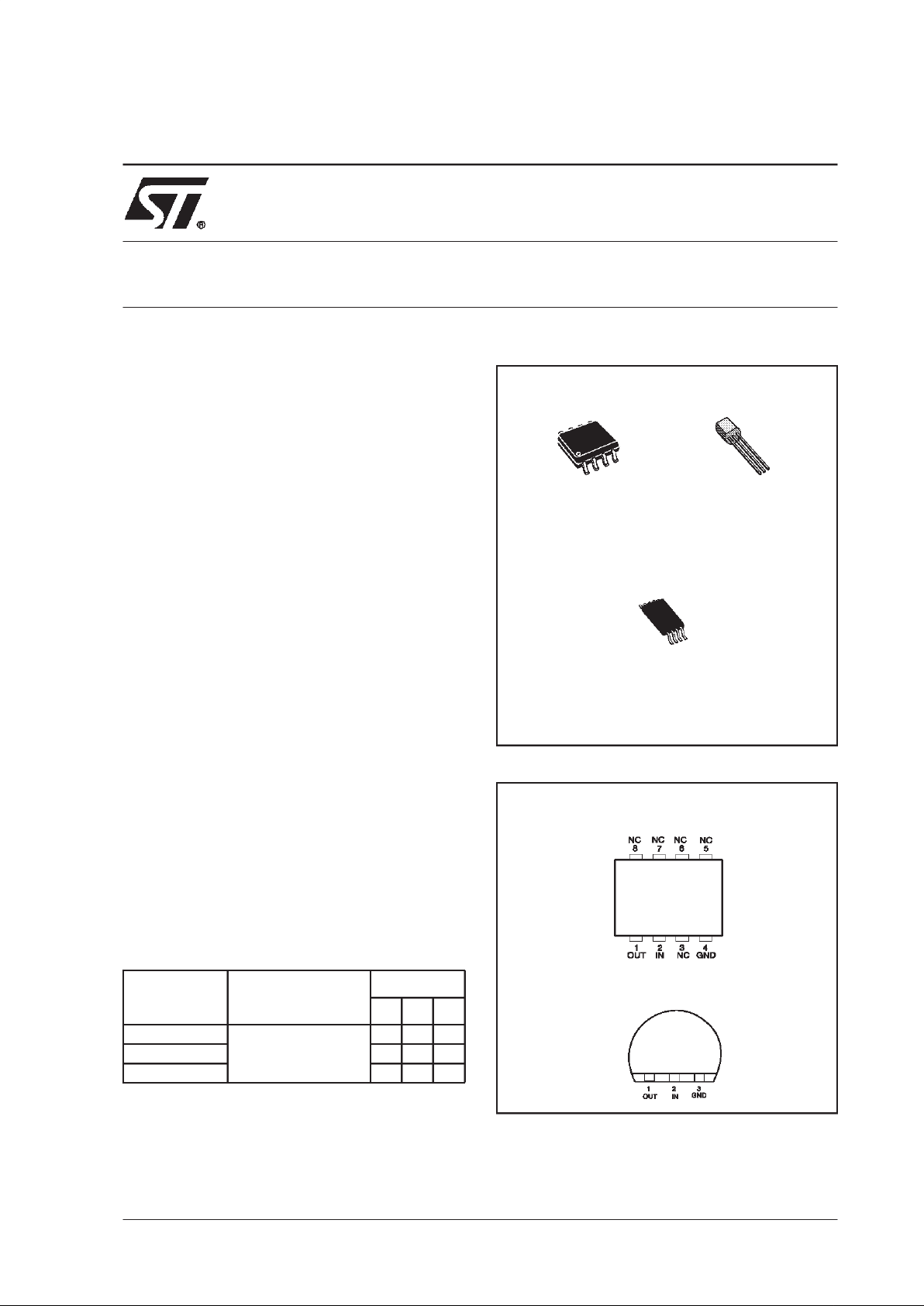
Z= TO92 Plastic package
D=Small Outline Package (SO) - also available in Tape & Reel (DT)
P=Thin Shrink Small Outline Package (TSSOP) - only available
in Tape & Reel (PT)
PIN CONNECTIONS (top view)
Part Number Temperature Range
Package
DZP
TS831-5I
-40, +125°C
•••
TS831-4I •••
TS831-3I •••
D
DIP-8
(Plastic Micropackage)
P
TSSOP-8
(Thin Shrink Small Outline Package)
Z
TO-92
(Plastic Package)
TO-92
SO8-TSSOP8
TS831
MICROPOWER VOLTAGE SUPERVISOR
RESET ACTIVE LOW
March 2000
TS831
2/11
ABSOLUTE MAXIMUM RATINGS
OPERATING CONDITIONS
TS831-5
ELECTRICAL CHARACTERISTICS Tamb = 25°C (unless otherwise specified)
Symbol Parameter Value Unit
V
CC
Supply Voltage
1)
7V
V
out
Output Voltage
-0.3 to V
cc
+ 0.3
V
I
out
Output Sink Current TS831-5 and TS831-4
TS831-3
20
5
mA
Pd
Power Dissipation
2)
TO-92
SO-8
TSSOP-8
625
700
625
mW
I
F
Clamp Diode Forward Current, pin 1 to pin 2
3)
100 mA
T
oper
Operating Free Air Temperature Range -40 to +85 °C
T
stg
Storage Temperature -65 to +150 °C
1. All voltages values, except differential voltage are with respect to network ground terminal.
2. T
j
= 150°C, T
amb
=25oC with Rthja = 200oC/W for TO-92 package
Rthja = 175
o
C/W for SO8 package
Rthja = 200
o
C/W for TSSOP8 package
3. Maximum package power dissipation limits must be observed.
Symbol Parameter Value Unit
V
CC
Supply Voltage 1 to 5.5 V
Symbol Parameter Min. Typ. Max. Unit
V
thi
Threshold Voltage - VCCIncreasing
-40°C ≤ Tamb ≤ +85°C
-40°C ≤ Tamb ≤ +125°C
4.10
4.10
4.33
4.46
4.50
V
V
thd
Threshold Voltage - VCCDecreasing
-40°C ≤ Tamb ≤ +85°C
-40°C ≤ Tamb ≤ +125°C
4.10
4.06
4.21
4.46
4.46
V
V
hys
Hysteresis Voltage 50 100 200 mV
I
CC
Current Consumption VCC=5V
12 µA
V
OL
Low Level Output Voltage VCC=4V,IOL= 8mA
-40°C ≤ Tamb ≤ +85°C
-40°C ≤ Tamb ≤ +125°C
450 800
1000
1300
mV
I
OH
Low Level Output Voltage VCC=5V
-40°C ≤ Tamb ≤ +125°C
2 100
1000
nA
tphl
Response Time High to Low
R
L
= 10kΩ,CL= 15pF,VCC=V
thd
-10mV
20 µs
Note : Limits are 100% production tested at 25°C. Limits over temperature are guaranteed through correlation and by design.
TS831
3/11
TS831-4
ELECTRICAL CHARACTERISTICS Tamb = 25°C (unless otherwise specified)
TS831-3
ELECTRICAL CHARACTERISTICS Tamb = 25°C (unless otherwise specified)
Symbol Parameter Min. Typ. Max. Unit
V
thi
Threshold Voltage - VCCIncreasing
-40°C ≤ Tamb ≤ +85°C
-40°C ≤ Tamb ≤ +125°C
4.17
4.10
4.35
4.66
4.70
V
V
thd
Threshold Voltage - VCCDecreasing
-40°C ≤ Tamb ≤ +85°C
-40°C ≤ Tamb ≤ +125°C
4.17
4.13
4.4
4.66
4.66
V
V
hys
Hysteresis Voltage 50 100 200 mV
I
CC
Current Consumption VCC=5V
12 µA
V
OL
Low Level Output Voltage VCC=4V,IOL= 8mA
-40°C ≤ Tamb ≤ +85°C
-40°C ≤ Tamb ≤ +125°C
450 800
1000
1300
mV
I
OH
Low Level Output Voltage VCC=5V
-40°C ≤ Tamb ≤ +125°C
2 100
1000
nA
tphl
Response Time High to Low
R
L
= 10kΩ,CL= 15pF,VCC=V
thd
-10mV
20 µs
Note : Limits are 100% production tested at 25°C. Limits over temperature are guaranteed through correlation and by design.
Symbol Parameter Min. Typ. Max. Unit
V
thi
Threshold Voltage - VCCIncreasing
-40°C ≤ Tamb ≤ +125°C
2.55
2.71
2.8
V
V
thd
Threshold Voltage - VCCDecreasing
-40°C ≤ Tamb ≤ +125°C
2.55
2.65
2.8
V
V
hys
Hysteresis Voltage 30 60 100 mV
I
CC
Current Consumption VCC=3V
12 µA
V
OL
Low Level Output Voltage VCC= 2.4V,IOL= 1mA
-40°C ≤ Tamb ≤ +125°C
140 400
500
mV
I
OH
Low Level Output Voltage VCC=3V
-40°C ≤ Tamb ≤ +125°C
2 100
1000
nA
tphl
Response Time High to Low
R
L
= 10kΩ,CL= 15pF,VCC=V
thd
-10mV
20 µs
Note : Limits are 100% production tested at 25°C. Limits over temperature are guaranteed through correlation and by design.
TS831
4/11
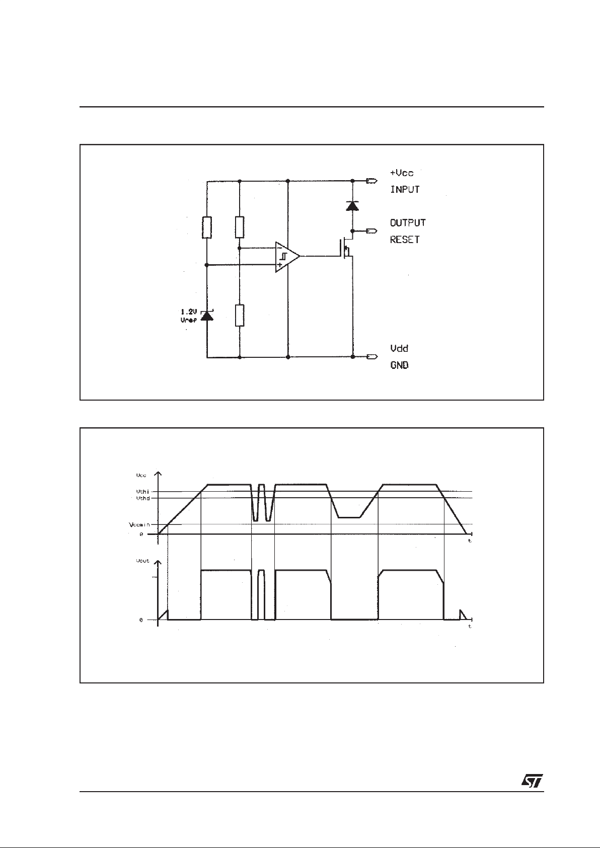
EQUIVALENT SCHEMATIC DIAGRAM
TIMING DIAGRAM
 Loading...