


KM416V256DLJ-5
Samsung KM416V256DLJ-5, KM416V256DJ-7, KM416V256DJ-6, KM416V256DJ-5, KM416V256DT-5 Datasheet
...
KM416C256D, KM416V256D CMOS DRAM
This is a family of 262,144 x 16 bit Fast Page Mode CMOS DRAMs. Fast Page Mode offers high speed random access of memory cells
within the same row. Power supply voltage (+5.0V or +3.3V), access time (-5,-6,-7), power consumption(Normal or Low power) and
package type(SOJ or TSOP-II) are optional features of this family. All of this family have CAS-before-RAS refresh, RAS-only refresh and
Hidden refresh capabilities. Furthermore, Self-refresh operation is available in L-version. This 256Kx16 fast page mode DRAM family is
fabricated using Samsung's advanced CMOS process to realize high band-width, low power consumption and high reliability.
It may be used as graphic memory unit for microcomputer, personal computer and portable machines.
¡Ü
Part Identification
- KM416C256D/DL (5V, 512K Ref.)
- KM416V256D/DL (3.3V, 512K Ref.)
¡Ü
Fast Page Mode operation
¡Ü
2 CAS Byte/Wrod Read/Write operation
¡Ü
CAS-before-RAS refresh capability
¡Ü
RAS-only and Hidden refresh capability
¡Ü
Self-refresh capability (L-ver only)
¡Ü
TTL(5V)/LVTTL(3.3V) compatible inputs and outputs
¡Ü
Early Write or output enable controlled write
¡Ü
JEDEC Standard pinout
¡Ü
Available in 40-pin SOJ 400mil and44(40)-pin
TSOP(II) 400mil packages
¡Ü
Triple +5V
¡¾
10% power supply(5V product)
¡Ü
Triple +3.3V
¡¾
0.3V power supply(3.3V product)
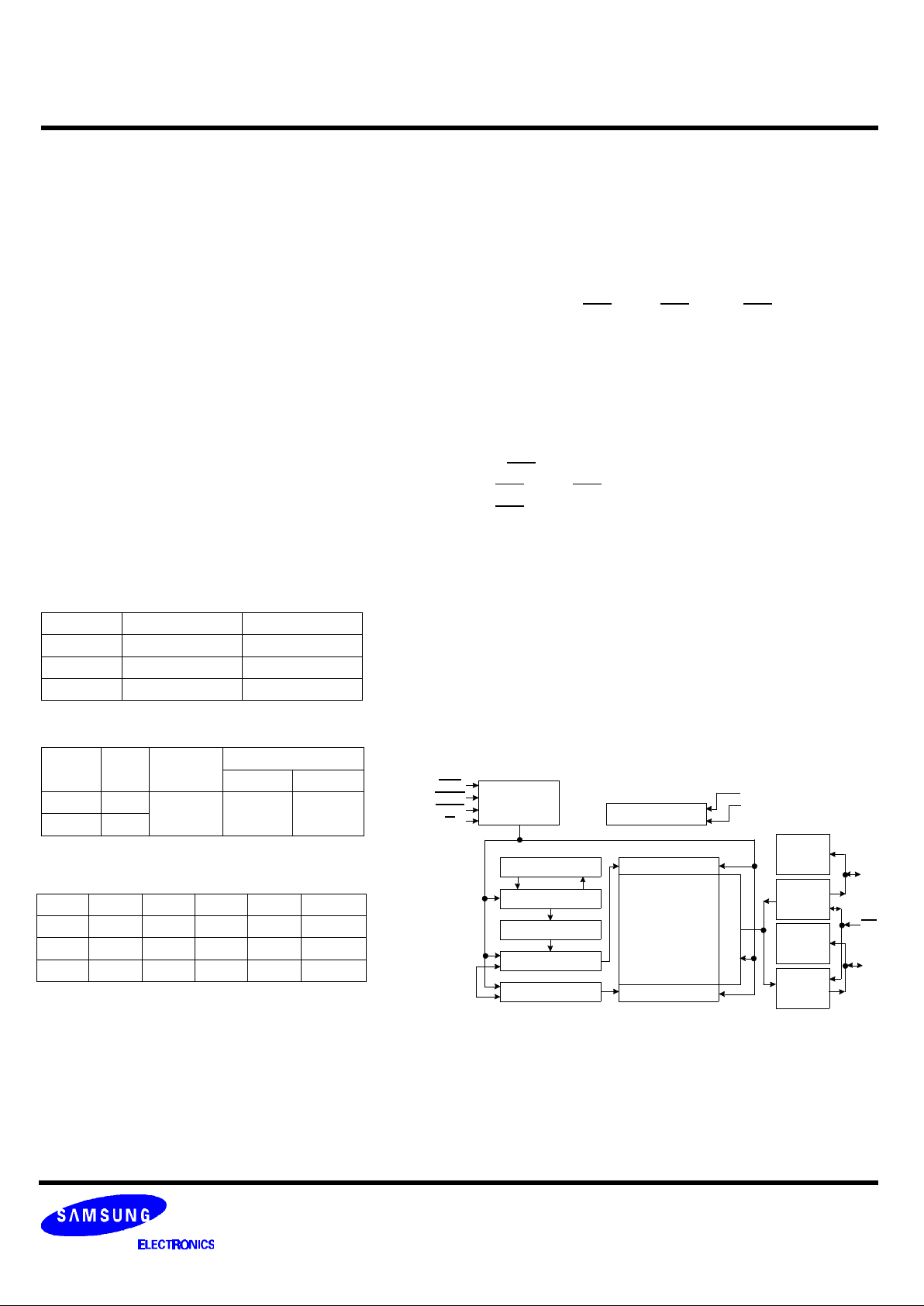
Control
Clocks
VBB Generator
Refresh Timer
Refresh Control
Refresh Counter
Row Address Buffer
Col. Address Buffer
Row Decoder
Column Decoder
Lower
Data out
Buffer
RAS
UCAS
LCAS
W
Vcc
Vss
DQ0
to
DQ7
A0
.
.
A8
Memory Array
262,144 x16
Cells
SAMSUNG ELECTRONICS CO., LTD. reserves the right to
change products and specifications without notice.
256K x 16Bit CMOS Dynamic RAM with Fast Page Mode
DESCRIPTION
FEATURES
FUNCTIONAL BLOCK DIAGRAM
¡Ü
Refresh Cycles
Part
NO.
VCC
Refresh
cycle
Refresh period
Normal L-ver
C256D 5V
512K 8ms 128ms
V256D 3.3V
¡Ü
Performance Range:
Speed
tRAC tCAC tRC tPC
Remark
-5 50ns 15ns 90ns 35ns 5V only
-6 60ns 15ns 10ns 40ns 5V/3.3V
-7 70ns 20ns 130ns 45ns 5V/3.3V
¡Ü
Active Power Dissipation
Speed 3.3V(512 Ref.) 5V(512 Ref.)
-5 - 605
-6 325 495
-7 290 440
Unit : mW
Sense Amps & I/O
Upper
Data in
Buffer
Upper
Data out
Buffer
Lower
Data in
Buffer
DQ8
to
DQ15
OE
KM416C256D, KM416V256D CMOS DRAM
VCC
DQ0
DQ1
DQ2
DQ3
VCC
DQ4
DQ5
DQ6
DQ7
N.C
N.C
W
RAS
N.C
A0
A1
A2
A3
VCC
VSS
DQ15
DQ14
DQ13
DQ12
VSS
DQ11
DQ10
DQ9
DQ8
N.C
LCAS
UCAS
OE
A8
A7
A6
A5
A4
VSS
1
2
3
4
5
6
7
8
9
10
11
12
13
14
15
16
17
18
19
20
40
39
38
37
36
35
34
33
32
31
30
29
28
27
26
25
24
23
22
21
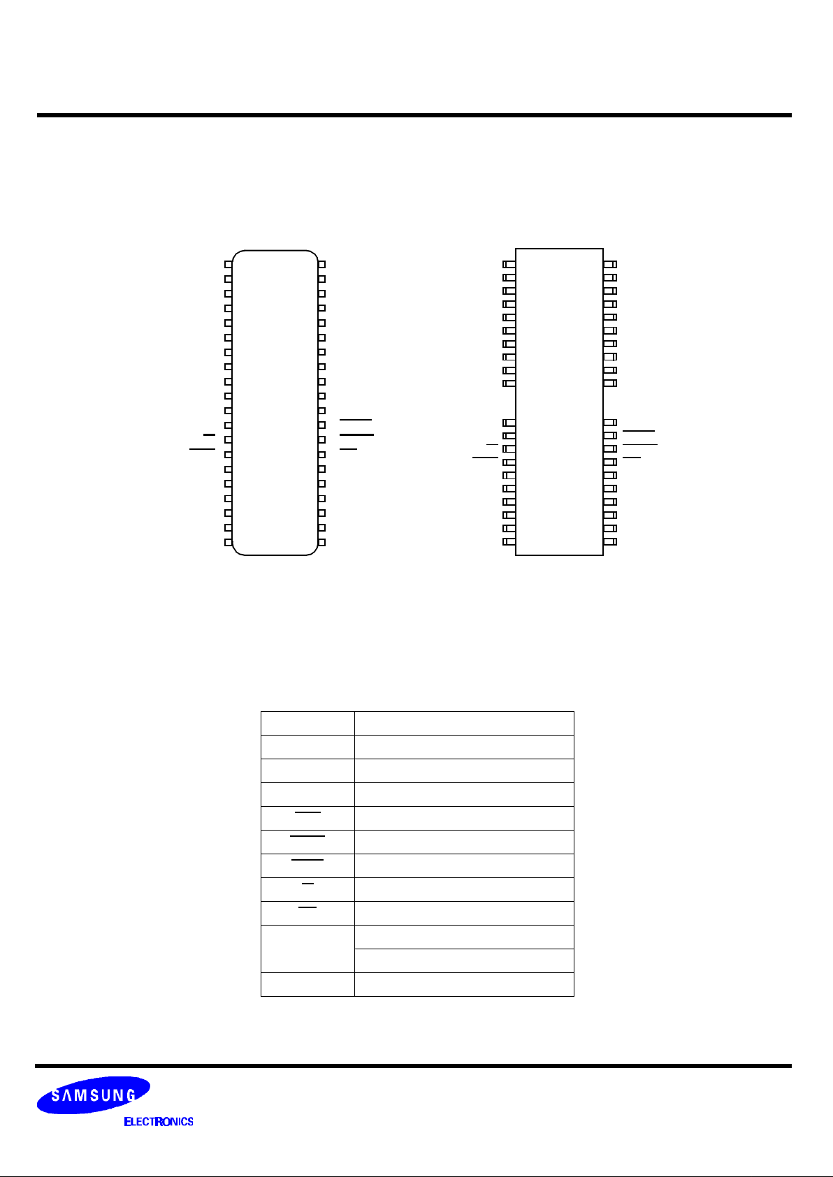
PIN CONFIGURATION (Top Views)
¡Ü
KM416C/V256DT
Pin Name Pin Function
A0 - A8 Address Inputs
DQ0 - 15 Data In/Out
VSS Ground
RAS Row Address Strobe
UCAS Upper Column Address Strobe
LCAS Lower Column Address Strobe
W Read/Write Input
OE Data Output Enable
VCC
Power(+5V)
Power(+3.3V)
N.C No Connection
¡Û
¡Û
VCC
DQ0
DQ1
DQ2
DQ3
VCC
DQ4
DQ5
DQ6
DQ7
N.C
N.C
W
RAS
N.C
A0
A1
A2
A3
VCC
VSS
DQ15
DQ14
DQ13
DQ12
VSS
DQ11
DQ10
DQ9
DQ8
N.C
LCAS
UCAS
OE
A8
A7
A6
A5
A4
VSS
1
2
3
4
5
6
7
8
9
10
11
12
13
14
15
16
17
18
19
20
40
39
38
37
36
35
34
33
32
31
30
29
28
27
26
25
24
23
22
21
¡Ü
KM416C/V256DJ
¡Û
¡Û
(SOJ) (TSOP-II)
KM416C256D, KM416V256D CMOS DRAM
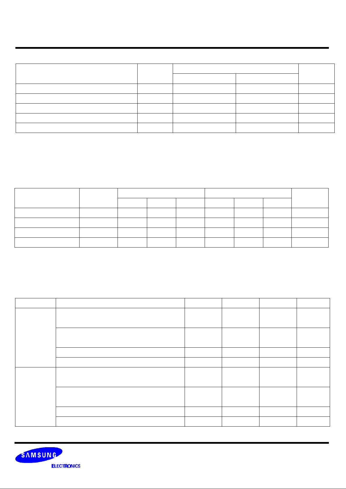
ABSOLUTE MAXIMUM RATINGS
* Permanent device damage may occur if "ABSOLUTE MAXIMUM RATINGS" are exceeded. Functional operation should be restricted to
the conditions as detailed in the operational sections of this data sheet. Exposure to absolute maximum rating conditions for ex
tended peri-
ods may affect device reliability.
Parameter Symbol
Rating
Units
3.3V 5V
Voltage on any pin relative to VSS VIN,VOUT -0.5 to +4.6 -1.0 to +7.0 V
Voltage on VCC supply relative to VSS VCC -0.5 to +4.6 -1.0 to +7.0 V
Storage Temperature Tstg -55 to +150 -55 to +150
¡É
Power Dissipation PD 1 1 W
Short Circuit Output Current IOS 50 50 mA
RECOMMENDED OPERATING CONDITIONS (Voltage referenced to Vss, TA= 0 to 70
¡É
)
*1 : VCC+1.3V/15ns(3.3V), VCC+2.0V/20ns(5V), Pulse width is measured at VCC
*2 : -1.3V/15ns(3.3V), -2.0V/20ns(5V), Pulse width is measured at VSS
Parameter Symbol
3.3V 5V
Units
Min Typ Max Min Typ Max
Supply Voltage VCC 3.0 3.3 3.6 4.5 5.0 5.5 V
Ground VSS 0 0 0 0 0 0 V
Input High Voltage VIH 2.0 - VCC+0.3 2.4 - VCC+1.0 V
Input Low Voltage VIL -0.3 - 0.8 -1.0 - 0.8 V
DC AND OPERATING CHARACTERISTICS (Recommended operating conditions unless otherwise noted.)
Max Parameter Symbol Min Max Units
3.3V
Input Leakage Current (Any input 0¡ÂVIN¡ÂVIN+0.3V,
all other input pins not under test=0 Volt)
II(L) -5 5 uA
Output Leakage Current
(Data out is disabled, 0V¡ÂVOUT¡ÂVCC)
IO(L) -5 5 uA
Output High Voltage Level(IOH=-2mA) VOH 2.4 - V
Output Low Voltage Level(IOL=2mA) VOL - 0.4 V
5V
Input Leakage Current (Any input 0¡ÂVIN¡ÂVIN+0.5V,
all other input pins not under test=0 Volt)
II(L) -5 5 uA
Output Leakage Current
(Data out is disabled, 0V¡ÂVOUT¡ÂVCC)
IO(L) -5 5 uA
Output High Voltage Level(IOH=-5mA) VOH 2.4 - V
Output Low Voltage Level(IOL=4.2mA) VOL - 0.4 V
*2
*1
*2
*1
 Loading...