


Samsung KS88P01416, KS88P01424, KS88C01424, KS88C01416, KS57P5616 Datasheet
...KS57C5616/P5616 |
PRODUCT OVERVIEW |
|
|
1 PRODUCT OVERVIEW
OVERVIEW
The KS57C5616/P5616 single-chip CMOS microcontroller is designed for high performance in the application for Caller-ID, Telephone using Samsung's newest 4-bit CPU core, SAM47 (Samsung Arrangable Microcontrollers).
Featuring a DTMF generator, up-to-960-dot LCD direct drive capability, one 8-bit timer/counter and flexible two 8-bit timer/counters, and serial I/O interface, the KS57C5616/P5616 offer an excellent design solution for a wide variety of applications requiring DTMF, LCD support.
Up to 43 (including COM/SEG) pins in the 100-pin QFP package can be dedicated to I/O. Nine vectored interrupts provide a fast response to internal and external events. In addition the advanced CMOS technology a of the KS57C5616/P5616 ensures low power consumption with a wide operating voltage range.
OTP
The KS57C5616 microcontroller is also available in OTP (One Time Programmable) version, KS57P5616. KS57P5616 microcontroller has an on-chip 16K-byte one-time-programmable EPROM instead of masked ROM. The KS57P5616 is comparable to KS57C5616, both in function and in pin configuration.
1-1

PRODUCT OVERVIEW |
KS57C5616/P5616 |
|
|
FEATURES SUMMARY
Memory
•16K × 8-bit ROM
•5,120 × 4-bit RAM (excluding LCD RAM)
I/O Pins
•Input only: 4pins (Not including COM/SEG)
6pins (Including COM/SEG)
• I/O: 15pins (Not including COM/SEG) 43pins (Including COM/SEG)
Memory-Mapped I/O Structure
•Data memory bank 15
8-bit Basic Timer
•Four interval timer functions
•Watchdog timer
8-bit Timer/Counter
•Programmable 8-bit timer
•External event counter
•Arbitrary clock frequency output
•External clock signal divider
16-Bit Timer/Counter
•Programmable 16-bit timer
•External event counter
•Arbitrary clock frequency output
•External clock signal divider
•Configurable as two 8-bit Timers
•Serial I/O interface clock generator
Watch Timer
•Time interval generation: 0.5 s, 3.9 ms at 32.768 kHz
•4 frequency outputs to BUZ pin (0.5, 1, 2, 4 kHz) at 32.768 kHz
Comparator
•4-channel mode: Internal reference (4-bit resolution); 16-step variable reference voltage
•3-channel mode: External reference
DTMF Generator
•16 dual-tone for tone dialing
8-bit Serial I/O Interface
•8-bit transmit/receive mode
•8-bit receive mode
•LSB-first or MSB-first transmission selectable
LCD Controller/Driver
•60 SEG x 16 COM terminals
•8, 12 and 16 com selectable
•COM 8–15: shared with port
•SEG40–59: shared with port
•Two kinds of LCD bias resistor value
Bit Sequential Carrier
•Supports 16-bit serial data transfer in arbitrary format
Interrupts
•Four external interrupt vectors
•Five internal interrupt vectors
•Two quasi-interrupts
Power-Down Modes
•Idle mode (only CPU clock stops)
•Stop mode (main system oscillation stops)
•Subsystem clock stop mode
Oscillation Sources
•RC, Crystal or Ceramic for system clock
•Oscillation frequency: 0.4–6.0 MHz
•CPU clock divider circuit (by 4, 8, or 64)
Instruction Execution Times
•1.12, 2.23, 17.88 µs at 3.58 MHz
•0.67, 1.33, 10.7 µs at 6.0 MHz
•122 µs at 32.768 kHz (subsystem)
Operating Temperature
•– 40 °C to 85 °C
Operating Voltage Range
• |
1.8 V |
to 5.5 V (except DTMF and Comparator) |
• |
2 V to |
5.5 V (include DTMF) |
•4.0 V to 5.5 V (include Comparator)
Package Type
•100-pin QFP (1420C)
1-2

KS57C5616/P5616 |
PRODUCT OVERVIEW |
|
|
BLOCK DIAGRAM
P7.0/SEG55/CIN0 |
|
|
|
|
|
|
|
|
P7.1/SEG54/CIN1 |
Comparator |
|
|
|
|
|
Basic |
Watchdog |
P7.2/SEG53/CIN2 |
|
|
|
|
|
|||
|
|
XIN |
XOUT |
|
|
Timer |
Timer |
|
P7.3/SEG52/CIN3 |
|
|
|
|
||||
|
|
|
|
|
|
|
|
|
P1.0-P1.3/ |
Input Port 1 |
RESET |
XTIN |
XTOUT |
|
|
|
|
|
|
|
|
|
Watch |
|
||
INT0-INT4 |
|
|
|
|
|
|
||
|
|
|
|
|
|
|
||
|
|
|
|
|
|
Timer |
|
|
|
|
|
|
|
|
|
|
|
P2.0/CLO |
I/O Port 2 |
|
|
|
|
|
|
|
P2.1/VLC1 |
Interrupt |
|
|
Instruction |
|
VLC1 |
||
P2.2 |
|
Control |
Clock |
|
||||
|
Register |
|
|
|||||
P3.0/TCLO0 |
|
Block |
|
|
|
COM0-COM7 |
||
|
|
|
|
|
LCD |
|||
P3.1/TCLO1 |
I/O Port 3 |
|
|
|
|
|
P4.0-P5.3/ |
|
P3.2/TCL0 |
|
|
|
|
|
Driver/ |
||
|
|
|
|
|
|
COM8-COM15 |
||
P3.3/TCL1 |
|
|
|
|
|
|
Controller |
|
|
|
|
|
|
|
SEG0-SEG39 |
||
P4.0-P4.3/ |
|
Internal |
|
|
Program |
|
||
I/O Port 4 |
|
|
|
P10.3-P6.0/ |
||||
|
|
Counter |
|
|||||
COM8-COM11 |
Interrupts |
|
|
|
||||
|
|
|
|
|
|
SEG40-SEG59 |
||
|
|
|
|
|
|
|
|
|
P5.0-P5.3/ |
I/O Port 5 |
|
|
|
|
|
|
|
COM12-COM15 |
|
|
|
|
|
|
|
|
|
|
|
|
|
|
Serial I/O |
|
|
|
|
Instruction Dcoder |
|
|
|
|||
P6.0-P6.3 |
|
Program |
|
|
||||
|
|
|
|
|
|
|||
SEG59-SEG56/ |
I/O Port 6 |
|
|
|
Status Word |
|
P0.0/SCK/KO |
|
KS4-KS7 |
|
|
|
|
||||
|
|
|
|
|
|
|
||
P7.0/SEG55/CIN0 |
I/O Port 7 |
Arithmetic |
|
|
|
I/O Port 0 |
P0.1/SO/K1 |
|
P7.1/SEG54/CIN1 |
and |
|
|
|
|
|
P0.2/SI/K2 |
|
|
|
|
|
Stack |
|
P0.3/BUZ/K3 |
||
P7.2/SEG53/CIN2 |
|
Logic Unit |
|
|
|
|||
|
|
|
|
|
||||
P7.3/SEG52/CIN3 |
|
|
|
|
Pointer |
DTMF |
|
|
|
|
|
|
|
|
|
DTMF |
|
P8.0/SEG51/LCDCK |
|
|
|
|
|
|
Generator |
|
|
|
|
|
|
|
|
||
P8.1/SEG50/LCDSY |
|
|
|
|
|
|
|
|
P8.2/SEG49 |
I/O Port 8 |
|
|
|
|
|
|
|
P8.3/SEG48 |
|
|
|
|
|
5K x 4-bit |
|
|
P9.0-P9.3/ |
I/O Port 9 |
|
|
16-Bit |
|
|
|
|
8-Bit |
|
|
RAM |
|
|
|||
SEG47-SEG44 |
|
|
Timer/Counter |
|
|
|||
|
Timer/ |
|
|
|
|
|||
|
|
|
(Two 8Bit |
|
|
|
|
|
|
|
Counter |
|
|
|
|
|
|
P10.0-P10.3/ |
I/O Port 10 |
Timer/Counter) |
16KB ROM |
|
|
|||
|
|
|
||||||
SEG43-SEG40 |
|
|
|
|
|
|
|
|
|
|
|
|
|
|
|
|
|
|
|
Figure 1-1. KS57C5616 Block Diagram |
|
|
||||
1-3
PRODUCT OVERVIEW |
KS57C5616/P5616 |
|
|
PIN ASSIGNMENTS
SEG8
SEG7
SEG6
SEG5
SEG4
SEG3
SEG2
SEG1
SEG0
DTMF P0.0/SCK/K0 P0.1/SO/K1 P0.2/SI/K2 P0.3/BUZ/K3
VDD
VSS
XOUT XIN
TEST
XTIN
XTOUT
RESET
P1.0/INT0
P1.1/INT1
P1.2/INT2
P1.3/INT4
P2.0/CLO
P2.1/VLC1
P2.2
P3.0/TCLO0
|
|
|
SEG9 |
|
SEG10 |
|
SEG11 |
|
SEG12 |
|
SEG13 |
|
SEG14 |
|
SEG15 |
|
SEG16 |
|
SEG17 |
|
SEG18 |
|
SEG19 |
|
SEG20 |
|
SEG21 |
|
SEG22 |
|
SEG23 |
|
SEG24 |
|
SEG25 |
|
SEG26 |
|
SEG27 |
|
SEG28 |
|
|
|||||||||||||||||||||||||||
|
|
|
|
|
|
|
|
|
|
|
|
|
|
|
|
|
|
|
|
|
|
|
|
|
|
|
|
|
|
|
|
|
|
|
|
|
|
|
|
|
|
|
|
|
|
|
|
|
|
|
|
|
|
|
|
|
|
|
|
|
|
|
|
|
|
|
|
|
|
|
|
|
|
|
|
|
|
|
|
|
|
|
|
|
|
|
|
|
|
|
|
|
|
|
|
|
|
|
|
|
|
|
|
|
|
|
|
|
|
|
|
|
|
|
|
|
|
|
|
|
|
|
|
|
|
|
|
|
|
|
|
|
|
|
|
|
|
|
|
|
|
|
|
100 |
99 |
98 |
97 |
96 |
95 |
94 |
93 |
92 |
91 |
90 |
89 |
88 |
87 |
86 |
85 |
84 |
83 |
82 |
81 |
|
|
|||||||||||||||||||||||||||||||||||||||||||||||
|
|
1 |
|
|
|
|
|
|
|
|
|
|
|
|
|
|
|
|
|
|
|
|
|
|
|
|
|
|
|
|
|
|
|
|
|
|
|
|
|
|
|
|
|
|
|
|
|
|
|
|
|
|
|
|
|
|
|
|
|
|
|
|
|
|
|
80 |
|
|
||
|
|
2 |
|
|
|
|
|
|
|
|
|
|
|
|
|
|
|
|
|
|
|
|
|
|
|
|
|
|
|
|
|
|
|
|
|
|
|
|
|
|
|
|
|
|
|
|
|
|
|
|
|
|
|
|
|
|
|
|
|
|
|
|
|
|
|
79 |
|
|
||
|
|
3 |
|
|
|
|
|
|
|
|
|
|
|
|
|
|
|
|
|
|
|
|
|
|
|
|
|
|
|
|
|
|
|
|
|
|
|
|
|
|
|
|
|
|
|
|
|
|
|
|
|
|
|
|
|
|
|
|
|
|
|
|
|
|
|
78 |
|
|
||
|
|
4 |
|
|
|
|
|
|
|
|
|
|
|
|
|
|
|
|
|
|
|
|
|
|
|
|
|
|
|
|
|
|
|
|
|
|
|
|
|
|
|
|
|
|
|
|
|
|
|
|
|
|
|
|
|
|
|
|
|
|
|
|
|
|
|
77 |
|
|
||
|
|
|
|
|
|
|
|
|
|
|
|
|
|
|
|
|
|
|
|
|
|
|
|
|
|
|
|
|
|
|
|
|
|
|
|
|
|
|
|
|
|
|
|
|
|
|
|
|
|
|
|
|
|
|
|
|
|
|
|
|
|
|
|
|
|
|
||||
|
|
5 |
|
|
|
|
|
|
|
|
|
|
|
|
|
|
|
|
|
|
|
|
|
|
|
|
|
|
|
|
|
|
|
|
|
|
|
|
|
|
|
|
|
|
|
|
|
|
|
|
|
|
|
|
|
|
|
|
|
|
|
|
|
|
|
76 |
|
|
||
|
|
|
|
|
|
|
|
|
|
|
|
|
|
|
|
|
|
|
|
|
|
|
|
|
|
|
|
|
|
|
|
|
|
|
|
|
|
|
|
|
|
|
|
|
|
|
|
|
|
|
|
|
|
|
|
|
|
|
|
|
|
|
|
|
|
|
||||
|
|
6 |
|
|
|
|
|
|
|
|
|
|
|
|
|
|
|
|
|
|
|
|
|
|
|
|
|
|
|
|
|
|
|
|
|
|
|
|
|
|
|
|
|
|
|
|
|
|
|
|
|
|
|
|
|
|
|
|
|
|
|
|
|
|
|
75 |
|
|
||
|
|
|
|
|
|
|
|
|
|
|
|
|
|
|
|
|
|
|
|
|
|
|
|
|
|
|
|
|
|
|
|
|
|
|
|
|
|
|
|
|
|
|
|
|
|
|
|
|
|
|
|
|
|
|
|
|
|
|
|
|
|
|
|
|
|
|
||||
|
|
7 |
|
|
|
|
|
|
|
|
|
|
|
|
|
|
|
|
|
|
|
|
|
|
|
|
|
|
|
|
|
|
|
|
|
|
|
|
|
|
|
|
|
|
|
|
|
|
|
|
|
|
|
|
|
|
|
|
|
|
|
|
|
|
|
74 |
|
|
||
|
|
|
|
|
|
|
|
|
|
|
|
|
|
|
|
|
|
|
|
|
|
|
|
|
|
|
|
|
|
|
|
|
|
|
|
|
|
|
|
|
|
|
|
|
|
|
|
|
|
|
|
|
|
|
|
|
|
|
|
|
|
|
|
|
|
|
||||
|
|
8 |
|
|
|
|
|
|
|
|
|
|
|
|
|
|
|
|
|
|
|
|
|
|
|
|
|
|
|
|
|
|
|
|
|
|
|
|
|
|
|
|
|
|
|
|
|
|
|
|
|
|
|
|
|
|
|
|
|
|
|
|
|
|
|
73 |
|
|
||
|
|
|
|
|
|
|
|
|
|
|
|
|
|
|
|
|
|
|
|
|
|
|
|
|
|
|
|
|
|
|
|
|
|
|
|
|
|
|
|
|
|
|
|
|
|
|
|
|
|
|
|
|
|
|
|
|
|
|
|
|
|
|
|
|
|
|
||||
|
|
9 |
|
|
|
|
|
|
|
|
|
|
|
|
|
|
|
|
|
|
|
|
|
|
|
|
|
|
|
|
|
|
|
|
|
|
|
|
|
|
|
|
|
|
|
|
|
|
|
|
|
|
|
|
|
|
|
|
|
|
|
|
|
|
|
72 |
|
|
||
|
|
|
|
|
|
|
|
|
|
|
|
|
|
|
|
|
|
|
|
|
|
|
|
|
|
|
|
|
|
|
|
|
|
|
|
|
|
|
|
|
|
|
|
|
|
|
|
|
|
|
|
|
|
|
|
|
|
|
|
|
|
|
|
|
|
|
||||
|
|
10 |
|
|
|
|
|
|
|
|
|
|
|
|
|
|
|
|
|
|
|
|
|
|
|
|
|
|
|
|
|
|
1420C)-QFP-(100 |
|
|
|
|
|
|
|
|
|
|
|
|
|
|
|
|
|
|
|
|
|
|
|
|
|
|
|
|
|
71 |
|
|
|||||
|
|
|
|
|
|
|
|
|
|
|
|
|
|
|
|
|
|
|
|
|
|
|
|
|
|
|
|
|
|
|
|
|
|
|
|
|
|
|
|
|
|
|
|
|
|
|
|
|
|
|
|
|
|
|
|
|
|
|
|
|
|
|
||||||||
|
|
11 |
|
|
|
|
|
|
|
|
|
|
|
|
|
|
|
|
|
|
|
|
|
|
|
|
|
|
|
|
|
|
|
|
|
|
|
|
|
|
|
|
|
|
|
|
|
|
|
|
|
|
|
|
|
|
|
|
|
|
|
70 |
|
|
||||||
|
|
|
|
|
|
|
|
|
|
|
|
|
|
|
|
|
|
|
|
|
|
|
|
|
|
|
|
|
|
|
|
|
|
|
|
|
|
|
|
|
|
|
|
|
|
|
|
|
|
|
|
|
|
|
|
|
|
|
|
|
|
|
||||||||
|
|
12 |
|
|
|
|
|
|
|
|
|
|
|
|
|
|
|
|
|
|
|
|
|
|
|
|
|
|
|
|
|
|
|
KS57C5616 |
|
|
|
|
|
|
|
|
|
|
|
|
|
|
|
|
|
|
|
|
|
69 |
|
|
||||||||||||
|
|
|
|
|
|
|
|
|
|
|
|
|
|
|
|
|
|
|
|
|
|
|
|
|
|
|
|
|
|
|
|
|
|
|
|
|
|
|
|
|
|
|
|
|
|
|
|
|
|
|
|
|
|
|
|
|||||||||||||||
|
|
13 |
|
|
|
|
|
|
|
|
|
|
|
|
|
|
|
|
|
|
|
|
|
|
|
|
|
|
|
|
|
|
|
|
|
|
|
|
|
|
|
|
|
|
|
|
|
|
|
|
|
|
|
|
68 |
|
|
|||||||||||||
|
|
|
|
|
|
|
|
|
|
|
|
|
|
|
|
|
|
|
|
|
|
|
|
|
|
|
|
|
|
|
|
|
|
|
|
|
|
|
|
|
|
|
|
|
|
|
|
|
|
|
|
|
|
|
|
|
|
|
|
|
|
|
|
|
|
|
||||
|
|
14 |
|
|
|
|
|
|
|
|
|
|
|
|
|
|
|
|
|
|
|
|
|
|
|
|
|
|
|
|
|
|
|
|
|
|
|
|
|
|
|
|
|
|
|
|
|
|
|
|
|
|
|
|
|
|
|
|
|
|
|
|
|
|
|
67 |
|
|
||
|
|
|
|
|
|
|
|
|
|
|
|
|
|
|
|
|
|
|
|
|
|
|
|
|
|
|
|
|
|
|
|
|
|
|
|
|
|
|
|
|
|
|
|
|
|
|
|
|
|
|
|
|
|
|
|
|
|
|
|
|
|
|
|
|
|
|
||||
|
|
15 |
|
|
|
|
|
|
|
|
|
|
|
|
|
|
|
|
|
|
|
|
|
|
|
|
|
|
|
|
|
|
|
|
|
|
|
|
|
|
|
|
|
|
|
|
|
|
|
|
|
|
|
|
|
|
|
|
|
|
|
|
|
|
|
66 |
|
|
||
|
|
|
|
|
|
|
|
|
|
|
|
|
|
|
|
|
|
|
|
|
|
|
|
|
|
|
|
|
|
|
|
|
|
|
|
|
|
|
|
|
|
|
|
|
|
|
|
|
|
|
|
|
|
|
|
|
|
|
|
|
|
|
|
|
|
|
||||
|
|
16 |
|
|
|
|
|
|
|
|
|
|
|
|
|
|
|
|
|
|
|
|
|
|
|
|
|
|
|
|
|
|
|
|
|
|
|
|
|
|
|
|
|
|
|
|
|
|
|
|
|
|
|
|
|
|
|
|
|
|
|
|
|
|
|
65 |
|
|
||
|
|
|
|
|
|
|
|
|
|
|
|
|
|
|
|
|
|
|
|
|
|
|
|
|
|
|
|
|
|
|
|
|
|
|
|
|
|
|
|
|
|
|
|
|
|
|
|
|
|
|
|
|
|
|
|
|
|
|
|
|
|
|
|
|
|
|
||||
|
|
17 |
|
|
|
|
|
|
|
|
|
|
|
|
|
|
|
|
|
|
|
|
|
|
|
|
|
|
|
|
|
|
|
|
|
|
|
|
|
|
|
|
|
|
|
|
|
|
|
|
|
|
|
|
|
|
|
|
|
|
|
|
|
|
|
64 |
|
|
||
|
|
|
|
|
|
|
|
|
|
|
|
|
|
|
|
|
|
|
|
|
|
|
|
|
|
|
|
|
|
|
|
|
|
|
|
|
|
|
|
|
|
|
|
|
|
|
|
|
|
|
|
|
|
|
|
|
|
|
|
|
|
|
|
|
|
|
||||
|
|
18 |
|
|
|
|
|
|
|
|
|
|
|
|
|
|
|
|
|
|
|
|
|
|
|
|
|
|
|
|
|
|
|
|
|
|
|
|
|
|
|
|
|
|
|
|
|
|
|
|
|
|
|
|
|
|
|
|
|
|
|
|
|
|
|
63 |
|
|
||
|
|
|
|
|
|
|
|
|
|
|
|
|
|
|
|
|
|
|
|
|
|
|
|
|
|
|
|
|
|
|
|
|
|
|
|
|
|
|
|
|
|
|
|
|
|
|
|
|
|
|
|
|
|
|
|
|
|
|
|
|
|
|
|
|
|
|
||||
|
|
19 |
|
|
|
|
|
|
|
|
|
|
|
|
|
|
|
|
|
|
|
|
|
|
|
|
|
|
|
|
|
|
|
|
|
|
|
|
|
|
|
|
|
|
|
|
|
|
|
|
|
|
|
|
|
|
|
|
|
|
|
|
|
|
|
62 |
|
|
||
|
|
|
|
|
|
|
|
|
|
|
|
|
|
|
|
|
|
|
|
|
|
|
|
|
|
|
|
|
|
|
|
|
|
|
|
|
|
|
|
|
|
|
|
|
|
|
|
|
|
|
|
|
|
|
|
|
|
|
|
|
|
|
|
|
|
|
||||
|
|
20 |
|
|
|
|
|
|
|
|
|
|
|
|
|
|
|
|
|
|
|
|
|
|
|
|
|
|
|
|
|
|
|
|
|
|
|
|
|
|
|
|
|
|
|
|
|
|
|
|
|
|
|
|
|
|
|
|
|
|
|
|
|
|
|
61 |
|
|
||
|
|
|
|
|
|
|
|
|
|
|
|
|
|
|
|
|
|
|
|
|
|
|
|
|
|
|
|
|
|
|
|
|
|
|
|
|
|
|
|
|
|
|
|
|
|
|
|
|
|
|
|
|
|
|
|
|
|
|
|
|
|
|
|
|
|
|
||||
|
|
21 |
|
|
|
|
|
|
|
|
|
|
|
|
|
|
|
|
|
|
|
|
|
|
|
|
|
|
|
|
|
|
|
|
|
|
|
|
|
|
|
|
|
|
|
|
|
|
|
|
|
|
|
|
|
|
|
|
|
|
|
|
|
|
|
60 |
|
|
||
|
|
|
|
|
|
|
|
|
|
|
|
|
|
|
|
|
|
|
|
|
|
|
|
|
|
|
|
|
|
|
|
|
|
|
|
|
|
|
|
|
|
|
|
|
|
|
|
|
|
|
|
|
|
|
|
|
|
|
|
|
|
|
|
|
|
|
||||
|
|
22 |
|
|
|
|
|
|
|
|
|
|
|
|
|
|
|
|
|
|
|
|
|
|
|
|
|
|
|
|
|
|
|
|
|
|
|
|
|
|
|
|
|
|
|
|
|
|
|
|
|
|
|
|
|
|
|
|
|
|
|
|
|
|
|
59 |
|
|
||
|
|
|
|
|
|
|
|
|
|
|
|
|
|
|
|
|
|
|
|
|
|
|
|
|
|
|
|
|
|
|
|
|
|
|
|
|
|
|
|
|
|
|
|
|
|
|
|
|
|
|
|
|
|
|
|
|
|
|
|
|
|
|
|
|
|
|
||||
|
|
23 |
|
|
|
|
|
|
|
|
|
|
|
|
|
|
|
|
|
|
|
|
|
|
|
|
|
|
|
|
|
|
|
|
|
|
|
|
|
|
|
|
|
|
|
|
|
|
|
|
|
|
|
|
|
|
|
|
|
|
|
|
|
|
|
58 |
|
|
||
|
|
|
|
|
|
|
|
|
|
|
|
|
|
|
|
|
|
|
|
|
|
|
|
|
|
|
|
|
|
|
|
|
|
|
|
|
|
|
|
|
|
|
|
|
|
|
|
|
|
|
|
|
|
|
|
|
|
|
|
|
|
|
|
|
|
|
||||
|
|
24 |
|
|
|
|
|
|
|
|
|
|
|
|
|
|
|
|
|
|
|
|
|
|
|
|
|
|
|
|
|
|
|
|
|
|
|
|
|
|
|
|
|
|
|
|
|
|
|
|
|
|
|
|
|
|
|
|
|
|
|
|
|
|
|
57 |
|
|
||
|
|
|
|
|
|
|
|
|
|
|
|
|
|
|
|
|
|
|
|
|
|
|
|
|
|
|
|
|
|
|
|
|
|
|
|
|
|
|
|
|
|
|
|
|
|
|
|
|
|
|
|
|
|
|
|
|
|
|
|
|
|
|
|
|
|
|
||||
|
|
25 |
|
|
|
|
|
|
|
|
|
|
|
|
|
|
|
|
|
|
|
|
|
|
|
|
|
|
|
|
|
|
|
|
|
|
|
|
|
|
|
|
|
|
|
|
|
|
|
|
|
|
|
|
|
|
|
|
|
|
|
|
|
|
|
56 |
|
|
||
|
|
|
|
|
|
|
|
|
|
|
|
|
|
|
|
|
|
|
|
|
|
|
|
|
|
|
|
|
|
|
|
|
|
|
|
|
|
|
|
|
|
|
|
|
|
|
|
|
|
|
|
|
|
|
|
|
|
|
|
|
|
|
|
|
|
|
||||
|
|
26 |
|
|
|
|
|
|
|
|
|
|
|
|
|
|
|
|
|
|
|
|
|
|
|
|
|
|
|
|
|
|
|
|
|
|
|
|
|
|
|
|
|
|
|
|
|
|
|
|
|
|
|
|
|
|
|
|
|
|
|
|
|
|
|
55 |
|
|
||
|
|
|
|
|
|
|
|
|
|
|
|
|
|
|
|
|
|
|
|
|
|
|
|
|
|
|
|
|
|
|
|
|
|
|
|
|
|
|
|
|
|
|
|
|
|
|
|
|
|
|
|
|
|
|
|
|
|
|
|
|
|
|
|
|
|
|
||||
|
|
27 |
|
|
|
|
|
|
|
|
|
|
|
|
|
|
|
|
|
|
|
|
|
|
|
|
|
|
|
|
|
|
|
|
|
|
|
|
|
|
|
|
|
|
|
|
|
|
|
|
|
|
|
|
|
|
|
|
|
|
|
|
|
|
|
54 |
|
|
||
|
|
|
|
|
|
|
|
|
|
|
|
|
|
|
|
|
|
|
|
|
|
|
|
|
|
|
|
|
|
|
|
|
|
|
|
|
|
|
|
|
|
|
|
|
|
|
|
|
|
|
|
|
|
|
|
|
|
|
|
|
|
|
|
|
|
|
||||
|
|
28 |
|
|
|
|
|
|
|
|
|
|
|
|
|
|
|
|
|
|
|
|
|
|
|
|
|
|
|
|
|
|
|
|
|
|
|
|
|
|
|
|
|
|
|
|
|
|
|
|
|
|
|
|
|
|
|
|
|
|
|
|
|
|
|
53 |
|
|
||
|
|
|
|
|
|
|
|
|
|
|
|
|
|
|
|
|
|
|
|
|
|
|
|
|
|
|
|
|
|
|
|
|
|
|
|
|
|
|
|
|
|
|
|
|
|
|
|
|
|
|
|
|
|
|
|
|
|
|
|
|
|
|
|
|
|
|
||||
|
|
29 |
|
|
|
|
|
|
|
|
|
|
|
|
|
|
|
|
|
|
|
|
|
|
|
|
|
|
|
|
|
|
|
|
|
|
|
|
|
|
|
|
|
|
|
|
|
|
|
|
|
|
|
|
|
|
|
|
|
|
|
|
|
|
|
52 |
|
|
||
|
|
|
|
|
|
|
|
|
|
|
|
|
|
|
|
|
|
|
|
|
|
|
|
|
|
|
|
|
|
|
|
|
|
|
|
|
|
|
|
|
|
|
|
|
|
|
|
|
|
|
|
|
|
|
|
|
|
|
|
|
|
|
|
|
|
|
||||
|
|
30 |
|
|
|
|
|
|
|
|
|
|
|
|
|
|
|
|
|
|
|
|
|
|
|
|
|
|
|
|
|
|
|
|
|
|
|
|
|
|
|
|
|
|
|
|
|
|
|
|
|
|
|
|
|
|
|
|
|
|
|
|
|
|
|
51 |
|
|
||
|
|
|
|
|
|
|
|
|
|
|
|
|
|
|
|
|
|
|
|
|
|
|
|
|
|
|
|
|
|
|
|
|
|
|
|
|
|
|
|
|
|
|
|
|
|
|
|
|
|
|
|
|
|
|
|
|
|
|
|
|
|
|
|
|
|
|
||||
|
|
31 |
|
32 |
|
33 |
|
34 |
|
35 |
|
36 |
|
37 |
|
38 |
|
39 |
40 |
|
41 |
|
42 |
|
43 |
|
44 |
|
45 |
|
46 |
|
47 |
|
48 |
|
49 |
|
50 |
|
|
|
||||||||||||||||||||||||||||
|
|
|
|
|
|
|
|
|
|
|
|
|
|
|
|
|
|
|
|
|
|
|
|
|
|
|
|
|
|
|
|
|
|
|
|
|
|
|
|
|
|
|
|
|
|
|
|
|
|
|
|
|
|
|
|
|
|
|
|
|
|
|
||||||||
|
|
|
|
|
|
|
|
|
|
|
|
|
|
|
|
|
|
|
|
|
|
|
|
|
|
|
|
|
|
|
|
|
|
|
|
|
|
|
|
|
|
|
|
|
|
|
|
|
|
|
|
|
|
|
|
|
|
|
|
|
|
|
|
|
|
|
|
|
|
|
|
|
P3.1/TCLO1 |
P3.2/TCL0 |
P3.3/TCL1 |
COM0 |
COM1 |
COM2 |
COM3 |
COM4 |
COM5 |
COM6 |
COM7 |
P4.0/COM8 |
P4.1/COM9 |
P4.2/COM10 |
P4.3/COM11 |
P5.0/COM12 |
P5.1/COM13 |
P5.2/COM14 |
P5.3/COM15 |
P6.0/SEG59/K4 |
|
|
|||||||||||||||||||||||||||||||||||||||||||||||
SEG29
SEG30
SEG31
SEG32
SEG33
SEG34
SEG35
SEG36
SEG37
SEG38
SEG39
P10.3/SEG40
P10.2/SEG41
P10.1/SEG42
P10.0/SEG43
P9.3/SEG44
P9.2/SEG45
P9.1/SEG46
P9.0/SEG47
P8.3/SEG48
P8.2/SEG49
P8.1/SEG50/LCDSY
P8.0/SEG51/LCDCK
P7.3/SEG52/CIN3
P7.2/SEG53/CIN2
P7.1/SEG54/CIN1
P7.0/SEG55/CIN0
P6.3/SEG56/K7
P6.2/SEG57/K6
P6.1/SEG58/K5
Figure 1-2. KS57C5616 Pin Assignments (100-QFP Package)
1-4
KS57C5616/P5616 PRODUCT OVERVIEW
PIN DESCRIPTIONS
Table 1-1. KS57C5616 Pin Descriptions
Pin Name |
Pin Type |
Description |
Share Pin |
|
|
|
|
P0.0 |
I/O |
4-bit I/O port. |
SCK/K0 |
P0.1 |
|
1-bit and 4-bit read/write and test is possible. |
SO/K1 |
P0.2 |
|
Individual pins are software configurable as input or |
SI/K2 |
P0.3 |
|
output. |
BUZ/K3 |
|
|
Individual pins are software configurable as open-drain or |
|
|
|
push-pull output. |
|
|
|
4-bit pull-up resistors are software assignable; pull-up |
|
|
|
resistors are automatically disabled for output pins. |
|
|
|
|
|
P1.0 |
I |
4-bit input port. |
INT0 |
P1.1 |
|
1-bit and 4-bit read and test is possible. |
INT1 |
P1.2 |
|
4-bit pull-up resistors are software assignable. |
INT2 |
P1.3 |
|
|
INT4 |
|
|
|
|
P2.0 |
I/O |
Same as port 0 except that port 2 is a 3-bit I/O port. |
CLO |
P2.1 |
|
|
VLC1 |
P2.2 |
|
|
|
|
|
|
|
P3.0 |
I/O |
Same as port 0. |
TCLO0 |
P3.1 |
|
|
TCLO1 |
P3.2 |
|
|
TCL0 |
P3.3 |
|
|
TCL1 |
|
|
|
|
P4.0–P4.3 |
I/O |
4-bit I/O ports. |
COM8–COM11 |
P5.0–P5.3 |
|
1-, 4-bit or 8-bit read/write and test is possible. |
COM12–COM15 |
|
|
Individual pins are software configurable as input or |
|
|
|
output. |
|
|
|
4-bit pull-up resistors are software assignable; pull-up |
|
|
|
resistors are automatically disabled for output pins. |
|
|
|
|
|
P6.0–P6.3 |
I/O |
Same as P4, P5. |
SEG59– |
|
|
|
SEG56/K4-K7 |
P7.0–P7.3 |
|
|
SEG55/CIN0– |
|
|
|
SEG52/CIN3 |
|
|
|
|
P8.0–P8.1 |
I/O |
Input ports. |
SEG51/LCDCK |
|
|
1-, 4-bit or 8-bit read and test is possible. |
SEG50/LCDSY |
|
|
4-bit pull-up resistors are software assignable; pull-up |
|
|
|
resistors are automatically disabled for output pins. |
|
|
|
These pins can not be used as push-pull output. Refer to |
|
|
|
the NOTES of Table 10-3. Port Mode Group Flags. |
|
|
|
|
|
P8.2–P8.3 |
I/O |
Same as P4, P5. |
SEG49 |
|
|
|
SEG48 |
P9.0–P9.3 |
|
|
SEG47–SEG44 |
|
|
|
|
P10.0–P10.3 |
I/O |
Same as P4, P5. |
SEG43–SEG40 |
|
|
|
|
SCK |
I/O |
Serial I/O interface clock signal. |
P0.0/K0 |
|
|
|
|
SO |
I/O |
Serial data output. |
P0.1/K1 |
|
|
|
|
|
|
|
|
1-5
PRODUCT OVERVIEW KS57C5616/P5616
Table 1-1. KS57C5616 Pin Descriptions (Continued)
Pin Name |
Pin Type |
Description |
Share Pin |
|
|
|
|
SI |
I/O |
Serial data input. |
P0.2/K2 |
|
|
|
|
BUZ |
I/O |
0.5, 1, 2, or 4 kHz frequency output for buzzer sound. |
P0.3/K3 |
|
|
|
|
INT0, INT1 |
I |
External interrupts. The triggering edge for INT0 and |
P1.0, P1.1 |
|
|
INT1 is selectable. |
|
|
|
|
|
INT2 |
I |
Quasi-interrupt with detection of rising or falling edges. |
P1.2 |
|
|
|
|
INT4 |
I |
External interrupt with a detection of rising and falling |
P1.3 |
|
|
edge. |
|
|
|
|
|
CLO |
I/O |
Clock output . |
P2.0 |
|
|
|
|
TCLO0 |
I/O |
Timer/counter 0 clock output. |
P3.0 |
|
|
|
|
TCLO1 |
I/O |
Timer/counter 1 clock output. |
P3.1 |
|
|
|
|
TCL0 |
I/O |
External clock input for timer/counter 0. |
P3.2 |
|
|
|
|
TCL1 |
I/O |
External clock input for timer/counter 1. |
P3.3 |
|
|
|
|
CIN0 |
I/O |
4-Channel comparator input |
P7.0/SEG55 |
CIN1 |
|
CIN0–CIN2: comparator input only |
P7.1/SEG54 |
CIN2 |
|
CIN3: comparator input or external reference input |
P7.2/SEG53 |
CIN3 |
|
|
P7.3/SEG52 |
|
|
|
|
DTMF |
O |
DTMF output |
– |
|
|
|
|
LCDCK |
I/O |
LCD clock output |
P8.0/SEG51 |
|
|
|
|
LCDSY |
I/O |
LCD synchronization clock output. |
P8.1/SEG50 |
|
|
|
|
COM0–COM7 |
O |
LCD common signal output. |
– |
|
|
|
|
COM8–COM11 |
I/O |
|
P4.0–P4.3 |
|
|
|
|
COM12–COM15 |
|
|
P5.0–P5.3 |
|
|
|
|
SEG0–SEG39 |
O |
LCD segment signal output. |
– |
|
|
|
|
SEG40–SEG59 |
I/O |
|
P10.3–P6.0 |
|
|
|
|
K0–K3 |
I/O |
External interrupt (triggering edge is selectable) |
P0.0–P0.3 |
|
|
|
|
K4–K7 |
|
|
P6.0–P6.3 |
|
|
|
|
VDD |
– |
Main power supply. |
– |
VSS |
– |
Ground. |
– |
RESET |
I |
Reset signal. |
– |
|
|
|
|
VLC1 |
– |
LCD power supply. |
P2.1 |
XIN, XOUT |
– |
Crystal, Ceramic or RC oscillator pins for system clock. |
– |
XTIN, XTOUT |
– |
Crystal oscillator pins for subsystem clock. |
– |
TEST |
I |
Chip test input pin. |
– |
|
|
Hold GND when the device is operating. |
|
|
|
|
|
NOTE: Pull-up resistors for all I/O ports are automatically disabled if they are configured to output mode.
1-6

KS57C5616/P5616 PRODUCT OVERVIEW
Table 1-2. Supplemental KS57C5616 Pin Data
Pin Names |
Share Pins |
I/O Type |
RESET Value |
Circuit Type |
|
|
|
|
|
P0.0–P0.3 |
SCK/K0, SO/K1, |
I/O |
Input |
E-4 |
|
SI/K2, BUZ/K3 |
|
|
|
|
|
|
|
|
P1.0–P1.3 |
INT0, INT1 and |
I |
Input |
A-4 |
|
INT2, INT4 |
|
|
|
|
|
|
|
|
P2.0 |
CLO |
I/O |
Input |
E-4 |
|
|
|
|
|
P2.1 |
VLC1 |
I/O |
Input |
E-7 |
|
|
|
|
|
P2.2 |
– |
I/O |
Input |
E-4 |
|
|
|
|
|
P3.0–P3.1 |
TCLO0, TCLO1 |
I/O |
Input |
E-2 |
|
|
|
|
|
P3.2–P3.3 |
TCL0, TCL1 |
I/O |
Input |
E-4 |
|
|
|
|
|
P4.0–P4.3 |
COM8–COM11 |
I/O |
Input |
H-24 |
P5.0–P5.3 |
COM12–COM15 |
|
|
|
|
|
|
|
|
P6.0–P6.3 |
SEG59/K4– |
I/O |
Input |
H-25 |
|
SEG56/K7 |
|
|
|
|
|
|
|
|
P7.0–P7.2 |
SEG55/CIN0– |
I/O |
Input |
H-26 |
|
SEG53/CIN2 |
|
|
|
|
|
|
|
|
P7.3 |
SEG52/CIN3 |
I/O |
Input |
H-27 |
|
|
|
|
|
P8.0–P8.1 |
SEG51–SEG50 |
I/O |
Input |
H-28 |
|
|
|
|
|
P8.2–P8.3 |
SEG49–SEG48 |
I/O |
Input |
H-24 |
|
|
|
|
|
P9.0–P9.3 |
SEG47–SEG44 |
I/O |
Input |
H-24 |
|
|
|
|
|
P10.0–P10.3 |
SEG43–SEG40 |
I/O |
Input |
H-24 |
|
|
|
|
|
COM0–COM7 |
– |
O |
High |
H-3 |
|
|
|
|
|
SEG0–SEG39 |
– |
O |
High |
H-3 |
|
|
|
|
|
DTMF |
– |
O |
High impedance |
G-7 |
|
|
|
|
|
VDD |
– |
– |
– |
– |
VSS |
– |
– |
– |
– |
RESET |
– |
I |
– |
B |
|
|
|
|
|
VLC1 |
– |
– |
– |
– |
XIN, XOUT |
– |
– |
– |
– |
XTIN, XTOUT |
– |
– |
– |
– |
TEST |
– |
I |
– |
– |
|
|
|
|
|
1-7

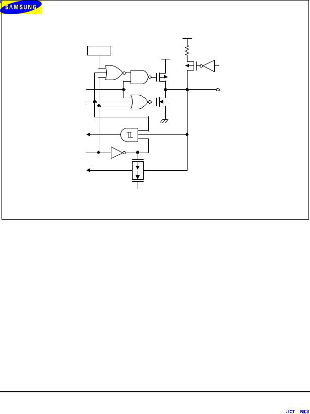
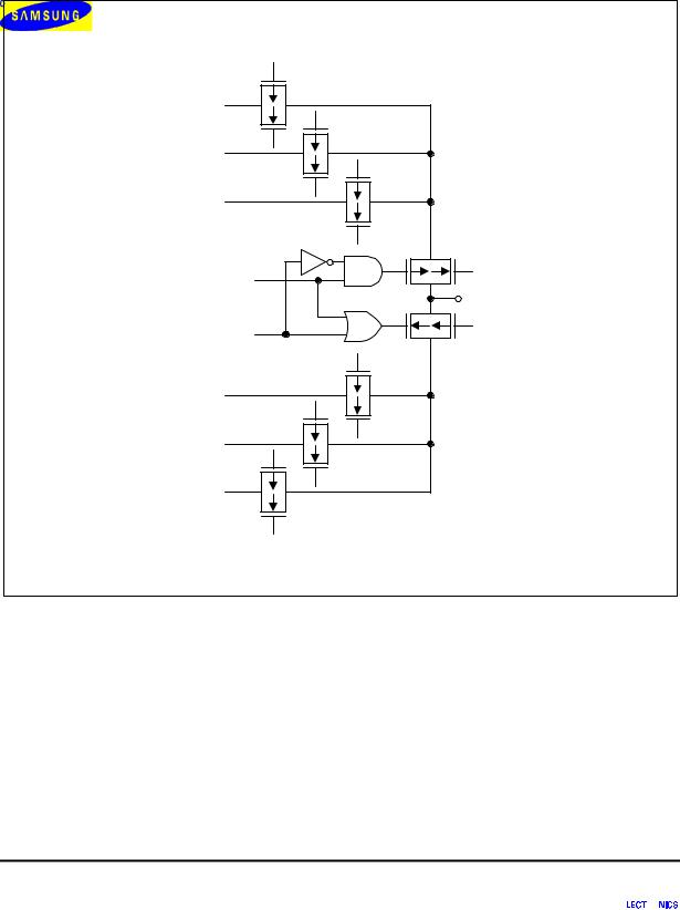
KS57C5616/P5616 (Preliminary Spec) |
PRODUCT OVERVIEW |
|
|
PIN CIRCUIT DIAGRAMS
VDD


 P-Channel
In 
N-Channel
Figure 1-3. Pin Circuit Type A
VDD
Pull-Up
Resistor
Pull-Up
Resistor
Enable
In
Schmitt Trigger
Figure 1-4. Pin Circuit Type A-4
VDD
Pull-Up
Resistor
In
Schmitt Trigger
Figure 1-5. Pin Circuit Type B
|
VDD |
Data |
P-CH |
|
|
|
Out |
Output |
N-CH |
DIsable |
|
Figure 1-6. Pin Circuit Type C
1-8

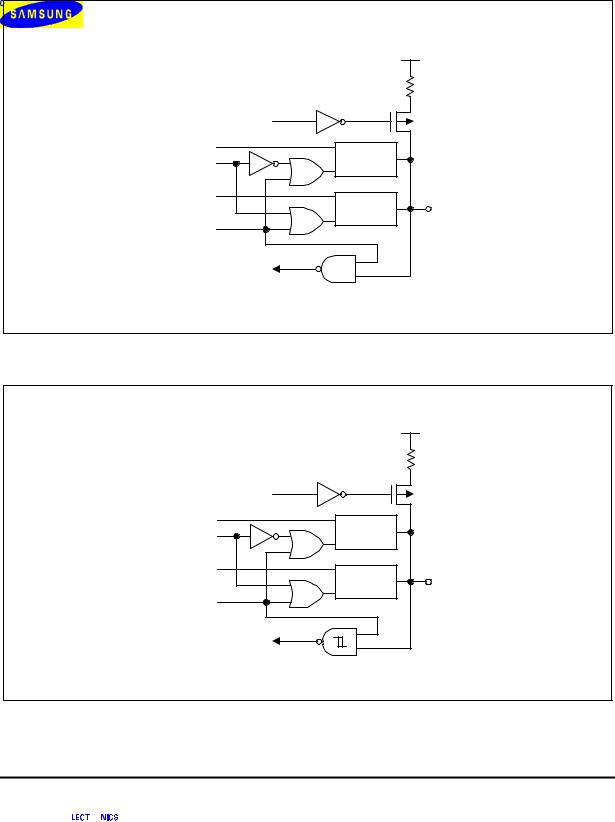
KS57C5616/P5616 |
PRODUCT OVERVIEW |
|
|
|
|
VDD |
|
PNE |
|
Pull-up |
|
VDD |
Resistor |
||
|
|||
|
|
Pull-up |
|
|
|
Resistor |
|
|
|
Enable |
|
|
|
P-CH |
|
Data |
|
I/O |
|
Output |
|
N-CH |
|
DIsable |
|
|
Figure 1-7. Pin Circuit Type E-2
|
|
VDD |
|
PNE |
|
Pull-up |
|
VDD |
Resistor |
||
|
|||
|
|
Pull-up |
|
|
|
Resistor |
|
|
|
Enable |
|
|
|
P-CH |
|
Data |
|
I/O |
|
Output |
|
N-CH |
|
DIsable |
|
|
Schmitt Trigger
Figure 1-8. Pin Circuit Type E-4
1-9
PRODUCT OVERVIEW |
KS57C5616/P5616 |
|
|
|
VDD |
|
PNE |
Pull-up |
|
Resistor |
||
VDD |
||
|
Pull-up |
|
|
Resistor |
|
|
Enable |
|
|
P-CH |
|
Data |
I/O |
|
Output |
N-CH |
|
DIsable |
||
|
||
Digital |
|
|
Input |
|
|
VLCEN |
|
|
VLC1 |
|
Figure 1-9. Pin Circuit Type E-7
1-10
KS57C5616/P5616 |
PRODUCT OVERVIEW |
|
|
VLC1
VLC2
VLC3
COM/SEG
VLC4
VLC5
VLC6
Figure 1-10. Pin Circuit Type H-3
1-11
PRODUCT OVERVIEW |
KS57C5616/P5616 |
|
|
VLC1
VLC2
VLC3
SEG/COM
Data
Out
Output
DIsable
VLC4
VLC5
VSS
Figure 1-11. Pin Circuit Type H-23
1-12
KS57C5616/P5616 |
PRODUCT OVERVIEW |
|
|
|
|
VDD |
|
Pull-up |
|
|
Resistor |
|
|
Pull-up |
|
|
Resistor |
|
COM/SEG |
Enable |
|
Circuit |
|
|
LCD_ON |
|
|
Type H-23 |
|
|
Data |
Circuit |
I/O |
|
||
|
Type C |
|
Output |
|
|
|
|
|
DIsable |
|
|
Figure 1-12. Pin Circuit Type H-24
|
|
VDD |
|
Pull-up |
|
|
Resistor |
|
|
Pull-up |
|
|
Resistor |
|
|
Enable |
|
COM/SEG |
Circuit |
|
LCD_ON |
|
|
Type H-23 |
|
|
Data |
Circuit |
I/O |
|
||
|
Type C |
|
Output |
|
|
|
|
|
DIsable |
|
|
Figure 1-13. Pin Circuit Type H-25
1-13
 Loading...