


KS88P2148T

KS88C2148/P2148 PRODUCT OVERVIEW
1-1
1 PRODUCT OVERVIEW
KS88-SERIES MICROCONTROLLES
Samsung's KS88 series of 8-bit single-chip CMOS microcontrollers offers a fast and efficient CPU, a wide range
of integrated peripherals, and various mask-programmable ROM sizes. Among the major CPU features are:
— Efficient register-oriented architecture
— Selectable CPU clock sources
— Idle and Stop power-down mode release by interrupt
— Built-in basic timer with watchdog function
A sophisticated interrupt structure recognizes up to eight interrupt levels. Each level can have one or more
interrupt sources and vectors. Fast interrupt processing (within a minimum of six CPU clocks) can be assigned to
specific interrupt levels.
KS88C2148/P2148 MICROCONTROLLER
The KS88C2148/P2148 single-chip CMOS
microcontroller is fabricated using the highly
advanced CMOS process, based on Samsung’s
newest CPU architecture.
The KS88C2148 is a microcontroller with a 48-Kbyte
mask-programmable ROM embedded.
The KS88P2148 is a microcontroller with a 48-Kbyte
one-time-programmable ROM embedded.
Using a proven modular design approach, Samsung
engineers have successfully developed the
KS88C2148/P2148 by integrating the following
peripheral modules with the powerful SAM8 core:
— Six programmable I/O ports, including five 8-bit
ports and one 7-bit port, for a total of 47 pins.
— Twelve bit-programmable pins for external
interrupts.
— One 8-bit basic timer for oscillation stabilization
and watchdog functions (system reset).
— One 8-bit timer/counter and one 16-bit
timer/counter with selectable operating modes.
— Watch timer for real time.
— 4-input A/D converter
— Serial I/O interface
The KS88C2148/P2148 is versatile microcontroller
for cordless phone, pager, etc. They are currently
available in 80-pin TQFP and 80-pin QFP package.
OTP
The KS88P2148 is an OTP (One Time Programmable) version of the KS88C2148 microcontroller. The
KS88P2148 microcontroller has an on-chip 48-Kbyte one-time-programmable EPROM instead of a masked ROM.
The KS88P2148 is comparable to the KS88C2148, both in function and in pin configuration.

PRODUCT OVERVIEW KS88C2148/P2148
1-2
FEATURES
CPU
• SAM8 CPU core
Memory
• Data memory: 1040-byte of internal register file
(Excluding LCD RAM)
• Program memory: 48-Kbyte internal program
memory (ROM)
External Interface
• 64-Kbyte external data memory area
Instruction Execution Time
• 750 ns at 8 MHz (minimum, Main oscillator)
• 183 µs at 32,768 Hz (minimum, Sub oscillator)
Interrupts
• 7 interrupt levels and 19 interrupt sources
• 19 vectors
• Fast interrupt processing feature (for one
selected interrupt level)
I/O Ports
• Five 8-bit I/O ports (P0-P4) and one 7-bit I/O
port (P5) for a total of 47 bit-programmable pins
8-Bit Basic Timer
• One programmable 8-bit basic timer (BT) for
oscillation stabilization control or watchdog timer
(software reset) function
Watch Timer
• Time internal generation: 3.91 ms, 0.5 s at
32,768 Hz
• Four frequency outputs to BUZ pin
• Clock source generation for LCD
Timers and Timer/Counters
• One 8-bit timer/counter (Timer 0) with three
operating modes: Interval, Capture, and PWM
• One 16-bit timer/counter (Timer 1) with two 8-bit
timer/counter modes
LCD Controller/Driver
• UP to 32 segment pins
• 3, 4, and 8 common selectable
• Choice of duty cycle
• All dots can be switched on/off
• Internal resistor circuit for LCD bias
Serial Port
• One synchronous SIO
A/D Converter
• 8-bit conversion resolution × 4 channel
• 34 µs conversion time(4 MHz CPU clock, fxx/4)
Oscillation Sources
• Crystal, ceramic, or RC for main system clock
• Crystal or external oscillator for subsystem clock
• Main system clock frequency: 8 MHz
• Subsystem clock frequency: 32.768 kHz
Power-Down Modes
• Main idle mode (only CPU clock stops)
• Sub idle mode
• Stop mode (main/sub system oscillation stops)
Operating Temperature Range
• – 40°C to + 85°C
Operating Voltage Range
• 2.0 V to 5.5 V at 32 kHz (sub clock)-6 MHz
(main clock)
• 2.2 V to 5.5 V at 8 MHz
Package Type
• 80-pin TQFP, 80-pin QFP
KS88C2148/P2148 PRODUCT OVERVIEW
1-3
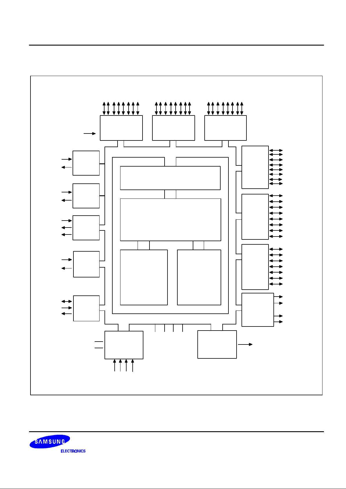
BLOCK DIAGRAM
I/O PORT and INTERRUPT
CONTROL
SAM8 CPU
INTERNAL BUS
PORT 3
48-KB ROM
1-KBYTE
REGISTER
FILE
PORT 0
P1.0-P1.7
PORT 1
TIMER 0
SIO
PORT 4
P0.0-P0.7
LCD
DRIVER
COM0-COM3
SEG0-SEG3/
COM4-COM7
SEG4-SEG31
VLC1
T1CK
TA
TB
BUZ
SCK
SI
SO
WATCH
TIMER
RESET
MAIN
OSC
SUB
OSC
TIMER 1
A and B
A/D
CONVERTER
PORT 5
P2.0-P2.7
PORT 2
P3.0-P3.7
P4.0-P4.7
P5.0-P5.6
VDD1 (INTERNAL)
VSS1 (INTERNAL)
VDD2 (EXTERNAL)
VSS2 (EXTERNAL)
ADC0-ADC3
AV
SS
AV
REF
T0CK
T0/T0CAP/
T0PWM
X
IN
X
OUT
X
IN
X
OUT
Figure 1-1. KS88C2148 Simplified Block Diagram
PRODUCT OVERVIEW KS88C2148/P2148
1-4
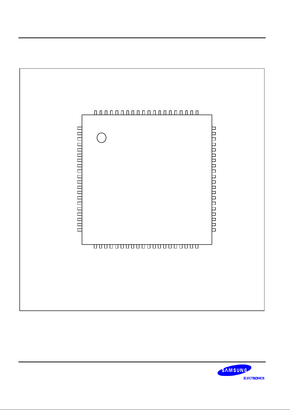
PIN ASSIGNMENTS
KS88C2148T
(80-TQFP-1212)
80
79
78
77
76
75
74
73
72
71
70
69
68
67
66
65
64
63
62
61
P1.0/SEG24/AD0
P0.7/SEG23/A15
P0.6/SEG22/A14
P0.5/SEG21/A13
P0.4/SEG20/A12
P0.3/SEG19/A11
P0.2/SEG18/A10
P0.1/SEG17/A9
P0.0/SEG16/A8
SEG15
SEG14
SEG13
SEG12
SEG11
SEG10
SEG9
SEG8
SEG7
SEG6
SEG5
1
2
3
4
5
6
7
8
9
10
11
12
13
14
15
16
17
18
19
20
P1.1/SEG25/AD1
P1.2/SEG26/AD2
P1.3/SEG27/AD3
P1.4/SEG28/AD4
P1.5/SEG29/AD5
P1.6/SEG30/AD6
P1.7/SEG31/AD7
P2.0/AS
P2.1/DR
VDD1 (INT)
VSS1
X
OUT
XIN
TEST
XTIN
XT
OUT
RESET
P2.2/
DW
P2.3/
DM
P2.4/INT0/T0CK
21
22
23
24
25
26
27
28
29
30
31
32
33
34
35
36
37
38
39
40
P2.5/INT1/T1CK
P2.6/INT2/TA
P2.7/INT3/TB
AV
REF
P3.0/ADC0
P3.1/ADC1
P3.2/ADC2
P3.3/ADC3
AV
SS
P3.4
P3.5
P3.6
P3.7/T0/T0PWM/T0CAP
P4.0/INT4
P4.1/INT5
P4.2/INT6
P4.3/INT7
P4.4/INT8
P4.5/INT9
P4.6/INT10
SEG4
SEG3/COM7
SEG2/COM6
SEG1/COM5
SEG0/COM4
COM3
COM2
COM1
COM0
VDD2(EXT)
VSS2
VLC1
P5.6
P5.5
P5.4
P5.3/BUZ
P5.2/SO
P5.1/SI
P5.0/SCK
P4.7/INT11
60
59
58
57
56
55
54
53
52
51
50
49
48
47
46
45
44
43
42
41
Figure 1-2. KS88C2148 Pin Assignments (80TQFP)
KS88C2148/P2148 PRODUCT OVERVIEW
1-5
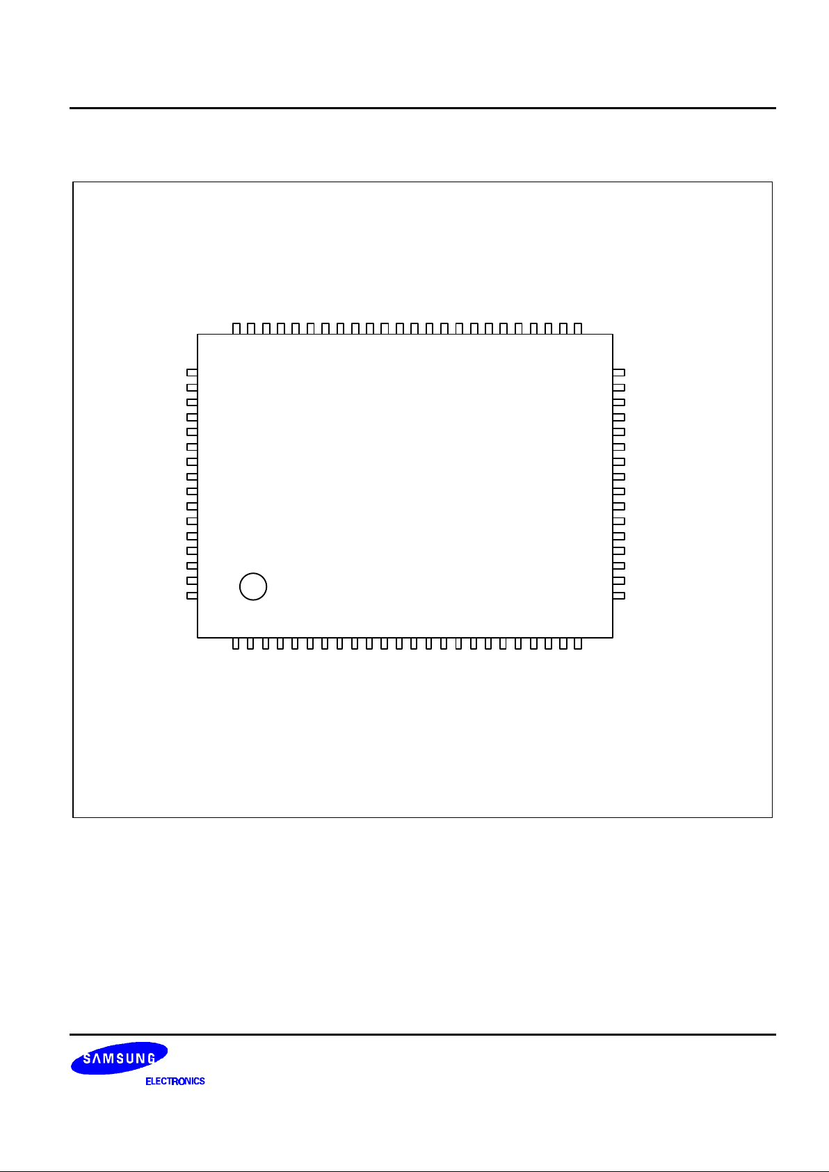
PIN ASSIGNMENTS (Continued)
KS88C2148Q
(80-QFP-1420C)
65
66
67
68
69
70
71
72
73
74
75
76
77
78
79
80
64
63
62
61
60
59
58
57
56
55
54
53
52
51
50
49
48
47
46
45
44
43
42
41
P4.4/INT8
P4.3/INT7
P4.2/INT6
P4.1/INT5
P4.0/INT4
P3.7/T0/T0PWM/T0CAP
P3.6
P3.5
P3.4
AVSS
P3.3/ADC3
P3.2/ADC2
P3.1/ADC1
P3.0/ADC0
AV
REF
P2.7/INT3/TB
SEG6
SEG5
SEG4
SEG3/COM7
SEG2/COM6
SEG1/COM5
SEG0/COM4
COM3
COM2
COM1
COM0
V
DD2
(EXT)
V
SS2
VLC1
P5.6
P5.5
P5.4
P5.3/BUZ
P5.2/SO
P5.1/SI
P5.0/SCK
P4.7/INT11
P4.6/INT10
P4.5/INT9
40
39
38
37
36
35
34
33
32
31
30
29
28
27
26
25
SEG7
SEG8
SEG9
SEG10
SEG11
SEG12
SEG13
SEG14
SEG15
P0.0/SEG16/A8
P0.1/SEG17/A9
P0.2/SEG18/A10
P0.3/SEG19/A11
P0.4/SEG20/A12
P0.5/SEG21/A13
P0.6/SEG22/A14
P0.7/SEG23/A15
P1.0/SEG24/AD0
P1.1/SEG25/AD1
P1.2/SEG26/AD2
P1.3/SEG27/AD3
P1.4/SEG28/AD4
P1.5/SEG29/AD5
P1.6/SEG30/AD6
P1.7/SEG31/AD7
P2.0/AS
P2.1/DR
V
DD1
(INT)
V
SS1
X
OUT
X
IN
TEST
XT
IN
XT
OUT
RESET
P2.2/DW
P2.3/DM
P2.4/INT0/T0CK
P2.5/INT1/T1CK
P2.6/INT2/TA
1 2 3 4 5 6 7 8 9
10
11
12
13
14
15
16
17
18
19
20
21
22
23
24
Figure 1-3. KS88C2148 Pin Assignments (80QFP)

PRODUCT OVERVIEW KS88C2148/P2148
1-6
PIN DESCRIPTIONS
Table 1-1. KS88C2148 Pin Descriptions
Pin
Names
Pin
Type
Pin
Description
Circuit
Type
Pin
Numbers
(note)
Share
Pins
P0.0-P0.7 I/O 4-bit-programmable I/O port.
Pull-up resistors and open-drain outputs
are software assignable. Pull-up resistors
are automatically disabled for output pins.
Configurable as LCD segments/ external
interface address and data lines
H-32 72-79
(74-80, 1)
SEG16/A8
–
SEG23/A15
P1.0-1.7 I/O 4-bit-programmable I/O port.
Pull-up resistors and open-drain outputs
are software assignable. Pull-up resistors
are automatically disabled for output pins.
Configurable as LCD segments/ external
interface address and data lines
H-32 80, 1-7
(2-9)
SEG24/AD0
–
SEG31/AD7
P2.0
P2.1
P2.2
P2.3
P2.4
P2.5
P2.6
P2.7
I/O
1-bit-programmable I/O port.
Pull-up resistors are software assignable,
and automatically disabled for output
pins. P2.0-P2.3 can alternately be used
as external interface lines. P2.4-P2.7 are
configurable as alternate functions or
external interrupts at falling edge with
noise filters.
D-4
8 (10)
9 (11)
18 (20)
19 (21)
20 (22)
21 (23)
22 (24)
23 (25)
AS
DR
DW
DM
INT0/T0CK
INT1/T1CK
INT2/TA
INT3/TB
P3.0-P3.3
P3.4-P3.6
P3.7
I/O 1-bit-programmable I/O port.
Pull-up resistors are software assignable,
and automatically disabled for output
pins. P3.0-P3.3 can alternately be used
as ADC. P3.7 is configurable as an
alternate function.
F-16
D-4
D-4
25-28
(27-30)
30-32
(32-34)
33 (35)
ADC0-ADC3
T0/T0PWM/
T0CAP
P4.0–P4.7 I/O 1-bit-programmable I/O port.
Pull-up resistors and open-drain outputs
are software assignable. Pull-up resistors
are automatically disabled for output pins.
P4.0-P4.7 are configurable as external
interrupts at a selectable edge with noise
filters.
E-4 34-41
(36-43)
INT4-INT11
P5.0
P5.1
P5.2
P5.3
P5.4-P5.6
I/O
1-bit-programmable I/O port.
Pull-up resistors are software assignable,
and automatically disabled for output
pins.
P5.0-P5.3 are configurable as alternate
functions. If SCK and SI are used as
input, these pins have noise filters.
D-4
42 (44)
43 (45)
44 (46)
45 (47)
46-48
(48-50)
SCK
SI
SO
BUZ
NOTE: Parentheses indicate pin number for 80-QFP package.
KS88C2148/P2148 PRODUCT OVERVIEW
1-7
Table 1-1. KS88C2148 Pin Descriptions (Continued)
Pin
Names
Pin
Type
Pin
Description
Circuit
Type
Pin
Numbers
(note)
Share
Pins
VSS1, VDD1
– Power input pins for internal power block – 10, 11 (12, 13) –
X
OUT
,
X
IN
– Main oscillator pins – 12, 13 (14, 15) –
TEST –
Chip test input pin
Hold GND when the device is operating
– 14 (16) –
XTIN, XT
OUT
– Sub oscillator pins for sub-system clock – 15,16 (17,18) –
RESET
I
RESET signal input pin. Schmitt trigger
input with internal pull-up resistor.
B 17 (19) –
INT0-INT3 I/O External interrupts input with noise filter. D-4 20-23 (22-25) P2.4–
P2.7
T0CK I/O 8Bit Timer 0 external clock input. D-4 20 (22) P2.4
T1CK I/O Timer 1/A external clock input. D-4 21 (23) P2.5
TA I/O Timer 1/A clock output D-4 22 (24) P2.6
TB I/O Timer B clock output D-4 23 (25) P2.7
T0 I/O Timer 0 clock output D-4 33 (35) P3.7
T0PWM I/O Timer 0 PWM output D-4 33 (35) P3.7
T0CAP I/O Timer 0 capture input D-4 33 (35) P3.7
ADC0-ADC3 I/O Analog input pins for A/D converts
module
F-16 25-28 (27-30) P3.0–
P3.3
AV
REF
, AV
SS
– A/D converter reference voltage and
ground
– 24, 29 (26, 31) –
INT4-INT11 I/O External interrupts input with noise filter. E-4 34-41 (36-43)
P4.0–
P4.7
BUZ I/O Buzzer signal output D-4 45 (47) P5.3
SCK, SI, SO I/O Serial clock, serial data input, serial data
output
D-4 42-44 (44-46) P5.0–
P5.2
VLC1
– LCD bias voltage input pins – 49 (51) –
VSS2, VDD2
– Power input pins for external power block – 50, 51 (52, 53) –
COM0-COM3 O LCD Common signal output H-30 52-55 (54-57) –
SEG0-SEG3
(COM4-COM7)
O LCD Common or Segment signal output H-31 56-59 (58-61) –
SEG4-SEG15 O LCD segment signal output H-29 60-71 (62-73) –
NOTE: Parentheses indicate pin number for 80-QFP package.

PRODUCT OVERVIEW KS88C2148/P2148
1-8
Table 1-1. KS88C2148 Pin Descriptions (Concluded)
Pin
Names
Pin
Type
Pin
Description
Circuit
Type
Pin
Numbers
Share
Pins
SEG16-SEG23 I/O LCD segment signal output H-32 72-79 (74-80, 1) P0.0-P0.7
SEG24-SEG31 I/O LCD segment signal output H-32 80, 1-7(2-9) P1.0-P1.7
A8-A15 I/O External interface address lines H-32 72-79(74-80, 1) P0.0-P0.7
AD0-AD7 I/O External interface address/data lines H-32 80, 1-7(2-9) P1.0-P1.7
AS
I/O Address strobe D-4 8 (10) P2.0
DR
I/O Data read D-4 9 (11) P2.1
DW
I/O Data write D-4 18 (20) P2.2
DM
I/O Data memory select D-4 19 (21) P2.3
NOTE: Parentheses indicate pin number for 80-QFP package.
KS88C2148/P2148 PRODUCT OVERVIEW
1-9
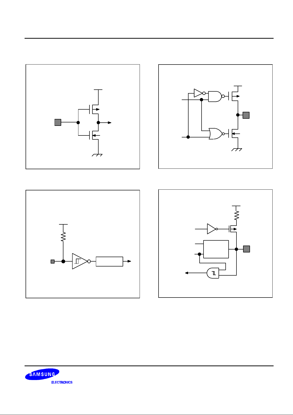
PIN CIRCUITS
V
DD
P-CHANNEL
N-CHANNEL
INPUT
Figure 1-4. Pin Circuit Type A
PULL-UP
RESISTOR
RESET
Noise Filter
V
DD
Figure 1-5. Pin Circuit Type B
OUTPUT
V
SS
DATA
OUTPUT
DISABLE
V
DD
Figure 1-6. Pin Circuit Type C
PULL-UP
ENABLE
DATA
OUTPUT
DISABLE
SCHMITT TRIGER
I/O
V
DD
CIRCUIT
TYPE C
Figure 1-7. Pin Circuit Type D-4
PRODUCT OVERVIEW KS88C2148/P2148
1-10
PULL-UP
RESISTOR
V
DD
I/O
V
SS
OPEN-DRAIN EN
PULL-UP
ENABLE
OUTPUT
DISABLE
V
DD
DATA
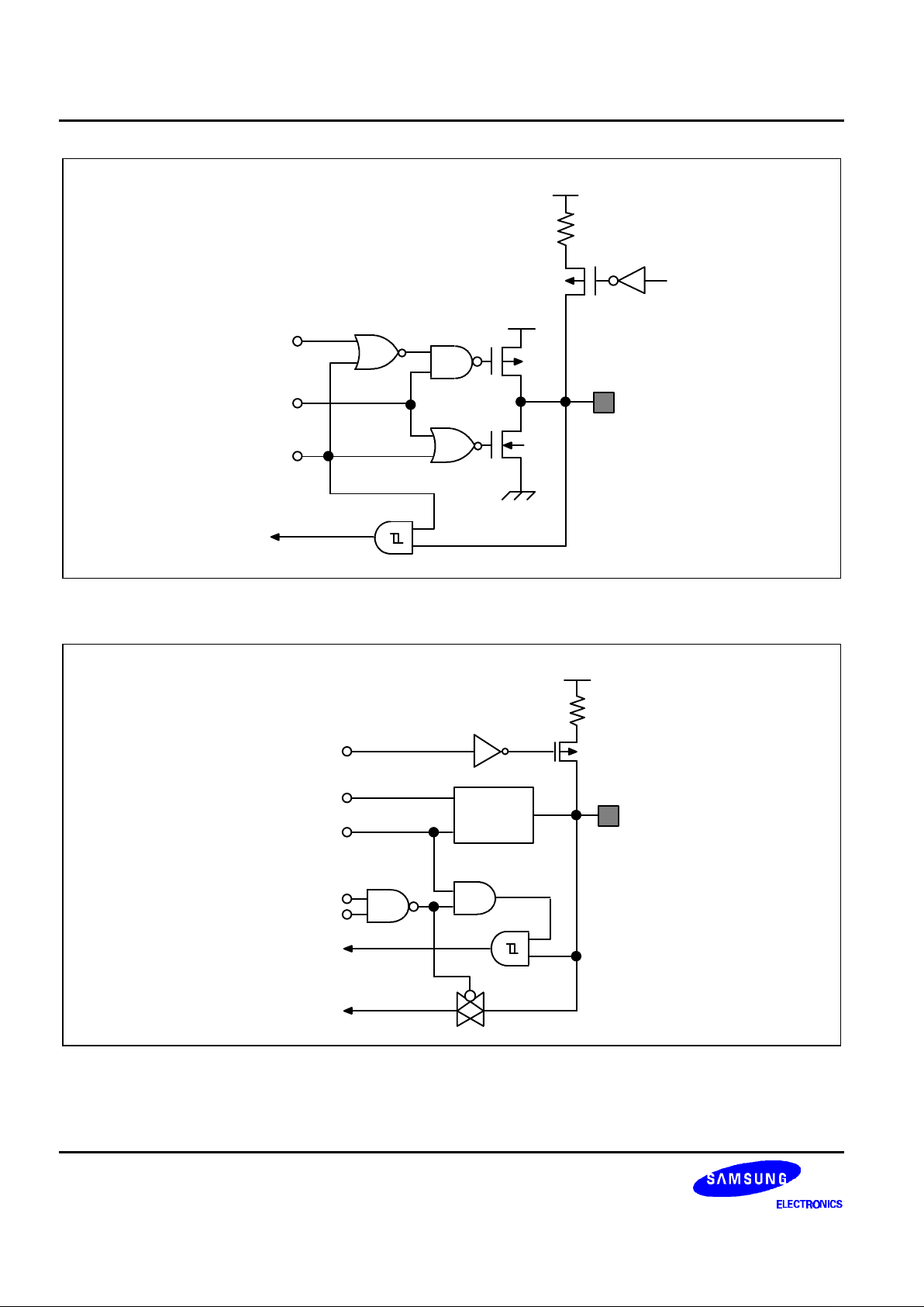
Figure 1-8. Pin Circuit Type E-4
PULL-UP
ENABLE
DATA
OUTPUT
DISABLE
I/O
V
DD
CIRCUIT
TYPE C
DATA
ADEN
ADSELECT
T0 ADC
Figure 1-9. Pin Circuit Type F-16

KS88C2148/P2148 PRODUCT OVERVIEW
1-11
V
LC1
V
LC3
V
SS
V
LC4
OUTPUT
Figure 1-10. Pin Circuit Type H-29
V
LC1
V
LC2
V
SS
V
LC5
OUTPUT
Figure 1-11. Pin Circuit Type H-30
V
LC1
V
LC2
OUTPUT
V
LC3
V
LC4
V
LC5
V
SS
Figure 1-12. Pin Circuit Type H-31
 Loading...