


KS88C6216/C6224/C6232/P6232 |
PRODUCT OVERVIEW |
|
|
1 PRODUCT OVERVIEW
SAM8 PRODUCT FAMILY
Samsung's SAM8 family of 8-bit single-chip CMOSmicrocontrollers offers a fast and efficient CPU with a wide range of integrated peripherals, in various mask-programmable ROM sizes. Analog its major CPU features are:
—Efficient register-oriented architecture
—Selectable CPU clock sources
—Idle and Stop power-down mode release by interrupt
—Built-in basic timer with watchdog function
The sophisticated interrupt structure recognizes up to eight interrupt levels. Each level can have one or more interrupt sources and vectors. Fast interrupt processing (within a minimum of six CPU clocks) can be assigned to specific interrupt levels.
KS88C6216/C6224/C6232/P6232 MICROCONTROLLERS
KS88C6216/C6224/C6232/P6232 single-chip 8-bit microcontrollers are based on the powerful SAM8 CPU architecture. The internal register file is logically expanded to increase the on-chip register space. KS88C6216/C6224/C6232/P6232 contain 16/32 K bytes of on-chip program ROM.
In line with Samsung's modular design approach, the following peripherals are integrated with the SAM8 core:
—Four programmable I/O ports (total 27 pins)
—One 8-bit basic timer for oscillation stabilization and watchdog functions
—One 8-bit general-purpose timer/counter with selectable clock sources
—One 12-bit counter with selectable clock sources, including Hsync or Csync input
—One interval timer
—PWM block with seven 8-bit PWM circuits
—Sync processor block (for Vsync and Hsync I/O, Csync input, and Clamp signal output)
—DDC and normal Multi-master IIC-bus
—4-channel A/D converter (8-bit resolution)
KS88C6216/C6224/C6232/P6232 are a versatile microcontrollers which are ideal for use in multi-sync monitors or in general-purpose applications that require sophisticated timer/counter, PWM, sync signal processing, A/D converter, and multi-master IIC-bus support with DDC. They are available in a 42pin SDIP or a 44-pin QFP package.
OTP
KS88C6216/C6224/C6232 microcontrollers are also available in OTP (One Time Programmable) version named, KS88P6232. KS88P6232 microcontroller has an on-chip 32-Kbyte one-time-programmable EPROM instead of masked ROM. KS88P6232 is comparable to KS88C6216/C6224/C6232, both in function and pin configuration except its ROM size.
1-1

PRODUCT OVERVIEW |
KS88C6216/C6224/C6232/P6232 |
|
|
FEATURES
CPU
•SAM8 CPU core
Memory
•16/24/32-Kbyte internal program memory (ROM)
•464-byte general-purpose register area
Instruction Set
•78 instructions
•IDLE and STOP instructions added for power-down modes
Instruction Execution Time
•Minimum 500 ns (with 12 MHz CPU clock)
Interrupts
•Ten interrupt sources
•Ten interrupt vectors
•Seven interrupt level
•Fast interrupt feature
General I/O
•Four I/O Ports (total 27pins)
8-Bit Basic Timer
•Programmable timer for oscillation stabilization interval control or watchdog timer function
•Three selective internal clock frequencies
Timer/Counters
•One 8-bit Timer/Counter with several clock sources (Capture mode)
•One 12-bit Counter with H-sync and several clock sources
•One Interval Timer
Pulse Width Modulator (PWM)
•8-bit PWM: 7-CH
Sync-Processor Block
•Vsync-I, Hsync-I, Csync-I input and Vsync-O, Hsync-O, Clamp-O output pins
•Pseudo sync signal output
•Auto SOG detection
•Auto Hsync polarity detection
DDC Multi-Master IIC-Bus 1-Ch
•Serial Peripheral Interface
•Support for Display Data Channel (DDC1/DDC2B/DDC2Bi/DDC2B+)
Normal Multi-Master IIC-Bus 1-Ch
•Serial Peripheral Interface
A/D Converter
•4-channel; 8-bit resolution
Oscillator Frequency
•8 MHz to 12 MHz crystal operation
•Internal Max. 12 MHz CPU clock
Operating Temperature Range
•– 40 °C to + 85 °C
Operating Voltage Range
•4.0 V to 5.5 V
Package Types
•42-pin SDIP, 44-pin QFP
1-2

KS88C6216/C6224/C6232/P6232 |
PRODUCT OVERVIEW |
|
|
BLOCK DIAGRAM
|
|
|
RESET |
|
|
|
||
XIN |
INT0-INT2 |
|
|
|
||||
|
|
|||||||
|
|
|
|
|
|
|
|
|
|
|
|
|
MAIN |
|
|||
|
|
|
|
|
||||
XOUT |
|
|
|
|
OSC |
|
||
|
|
|
|
|
||||
PWM0 |
|
|
|
|
|
|
|
|
|
|
|
|
|
|
|
|
|
|
|
|
|
|
|
|
|
|
• |
|
|
|
|
8-BIT |
|
||
|
|
|
|
|||||
• |
|
|
|
|
PWM |
|
||
|
|
|
|
|
||||
• |
|
|
|
|
|
|||
|
|
|
|
(7-CH) |
|
|||
• |
|
|
|
|
|
|||
|
|
|
|
|||||
PWM6 |
|
|
|
|
|
|
|
|
|
|
|
|
|
|
|
|
|
|
|
|
|
|
|
|
|
|
Vsync-I
Hsync-I
Csync-I  Sync-
Sync-
Vsync-O  Processor
Hsync-O
Clamp-O 
8-Bit
MT0CAP  Counter (Timer M0)
P0.0−P0.7/INT0 −INT2 |
P2.0−P2.7 |
VDD, AVREF
PORT 0 |
PORT 2 |
|
VSS1, V SS2 |
|
TEST
INTERNAL BUS

 PORT 1
 P1.0–P1.2 I/O PORT and INTERRUPT
CONTROL
PORT3 
 P3.0–P3.7
SAM8 CPU
|
|
|
|
|
|
|
|
|
|
|
|
|
|
|
|
|
|
|
|
|
|
|
|
ADC |
|
|
AD0−AD3 |
|
|
|
|
|
|
|
|
|
|
|
|
|
|
|
|
|
|
|
|
|
|
|
|
|
|
|
|||
|
|
|
|
|
|
|
|
|
|
|
|
|
|
|
|
|
|
|
|
|
|
|
|
|
|
|||
|
|
|
|
|
|
|
|
|
|
|
|
|
|
|
464-Byte |
|
|
|
|
|
|
|||||||
|
|
|
|
|
|
|
|
|
|
|
|
|
|
|
|
|
||||||||||||
|
|
|
|
16/24/32- |
|
|
|
|
|
|
|
|
|
|
|
|
|
|
|
|||||||||
|
|
|
|
|
Kbyte |
|
|
|
|
|
Register File |
|
|
|
|
|
|
|
|
|||||||||
|
|
|
|
|
|
|
|
|
|
|
|
|
|
|
|
|
|
|
||||||||||
|
|
|
|
|
ROM |
|
|
|
|
|
|
|
|
|
|
|
|
|
|
|
Multi |
|
|
SCL1 |
||||
|
|
|
|
|
|
|
|
|
|
|
|
|
|
|
|
|
|
|
|
|
|
|
|
Master |
|
|
||
|
|
|
|
|
|
|
|
|
|
|
|
|
|
|
|
|
|
|
|
|
|
|
|
|||||
|
|
|
|
|
|
|
|
|
|
|
|
|
|
|
|
|
|
|
|
|
|
|
|
|
|
SDA1 |
||
|
|
|
|
|
|
|
|
|
|
|
|
|
|
|
|
|
|
|
|
|
|
|
|
IIC-Bus |
|
|
||
|
|
|
|
|
|
|
|
|
|
|
|
|
|
|
|
|
|
|
|
|
|
|
|
|
|
|
|
|
|
|
|
|
|
|
|
|
|
|
|
|
|
|
|
|
|
|
|
|
|
|
|
|
|
|
|
|
|
|
12-Blt |
|
|
|
Interval |
|
|
Multi Master IIC-Bus |
|
|
|
|
||||||||||||||||
Counter |
|
|
|
Timer |
|
|
|
|
|
|
||||||||||||||||||
|
|
|
|
|
and DDC1/2B/2Bi/2B+ |
|
|
|
|
|||||||||||||||||||
(Timer M1) |
|
|
|
(Timer M2) |
|
|
|
|
|
|
||||||||||||||||||
|
|
|
|
|
|
|
|
|
|
|
|
|
|
|
|
|
|
|||||||||||
|
|
|
|
|
|
|
|
|
|
|
|
|
|
|
|
|
|
|
|
|
|
|
|
|
|
|
|
|
MT1CK |
SCL0 SDA0 |
Figure 1-1. Block Diagram
1-3
PRODUCT OVERVIEW |
KS88C6216/C6224/C6232/P6232 |
|
|
PIN ASSIGNMENTS
P0.0/INT0 |
|
1 |
|
|
|
42 |
|
P3.7 |
|
|
|
|
|
||||
|
|
|
|
|
||||
P0.1/INT1 |
|
2 |
|
|
|
41 |
|
P3.6 |
|
|
|
|
|
||||
P0.2/INT2 |
|
3 |
|
|
|
40 |
|
P3.5 |
|
|
|
|
|
||||
P0.3 |
|
4 |
|
|
|
39 |
|
P3.4 |
|
|
|
|
|
||||
P0.4/TM0CAP |
|
5 |
|
|
|
38 |
|
P3.3/AD3 |
|
|
|
|
|
||||
P0.5/TM1CK |
|
6 |
|
|
|
37 |
|
P3.2/AD2 |
|
|
|
|
|
||||
P0.6 |
|
7 |
|
|
|
36 |
|
P3.1/AD1 |
|
|
|
|
|
||||
P0.7 |
|
8 |
|
|
|
35 |
|
P3.0/AD0 |
|
|
|
|
|
||||
P1.0/SDA1 |
|
9 |
KS88C6216 |
34 |
|
AVREF |
||
|
|
|||||||
P1.1/SCL1 |
|
10 |
33 |
|
VSS2 |
|||
|
|
|||||||
|
/C6224/C6232 |
|
||||||
VDD |
|
11 |
32 |
|
P2.7/Csync-I |
|||
|
|
|||||||
|
42-SDIP |
|
||||||
|
|
|||||||
VSS1 |
|
12 |
31 |
|
Hsync-I |
|||
|
(Top View) |
|
||||||
|
|
|||||||
XOUT |
|
13 |
|
|
|
30 |
|
Vsync-I |
|
|
|
|
|
||||
XIN |
|
14 |
|
|
|
29 |
|
Vsync-O |
|
|
|
|
|
||||
TEST |
|
15 |
|
|
|
28 |
|
Hsync-O |
|
|
|
|
|
||||
SDA0 |
|
16 |
|
|
|
27 |
|
Clamp-O |
|
|
|
|
|
||||
SCL0 |
|
17 |
|
|
|
26 |
|
P2.6/PWM6 |
|
|
|
|
|
||||
RESET |
|
18 |
|
|
|
25 |
|
P2.5/PWM5 |
|
|
|
|
|
||||
P1.2 |
|
19 |
|
|
|
24 |
|
P2.4/PWM4 |
|
|
|
|
|
||||
P2.0/PWM0 |
|
20 |
|
|
|
23 |
|
P2.3/PWM3 |
|
|
|
|
|
||||
P2.1/PWM1 |
|
21 |
|
|
|
22 |
|
P2.2/PWM2 |
|
|
|
|
|
||||
|
|
|
|
|
|
|
|
|
Figure 1-2. KS88C6216/C6224/C6232 42-SDIP Pin Assignment
1-4
KS88C6216/C6224/C6232/P6232 |
PRODUCT OVERVIEW |
|
|
|
|
|
P0.4/TM0CAP |
P0.3 |
P0.2/INT2 |
P0.1/INT1 |
NC |
P0.0/INT0 |
P3.7 |
P3.6 |
P3.5 |
P3.4 |
P3.3/AD3 |
|
|
|
|||||||||||||||||||||
|
|
|
|
|
|
|
|
|
|
|
|
|
|
|
|
|
|||||||||||||||||||||
|
|
|
|
|
|
|
|
|
|
|
|
|
|
|
|
|
|
|
|
|
|
|
|
|
|
|
|
|
|
|
|
|
|
|
|
|
|
|
|
44 |
43 |
42 |
41 |
40 |
39 |
38 |
37 |
36 |
35 |
34 |
|
|
|
||||||||||||||||||||||
P0.5/TM1CK |
|
|
1 |
|
|
|
|
|
|
|
|
|
|
|
|
|
|
|
|
|
|
|
|
|
|
|
|
|
|
|
|
33 |
|
|
P3.2/AD2 |
||
|
|
|
|
|
|
|
|
|
|
|
|
|
|
|
|
|
|
|
|
|
|
|
|
|
|
|
|
|
|
|
|
||||||
P0.6 |
|
2 |
|
|
|
|
|
|
|
|
|
|
|
|
|
|
|
|
|
|
|
|
|
|
|
|
|
|
|
|
32 |
|
|
P3.1/AD1 |
|||
|
|
|
|
|
|
|
|
|
|
|
|
|
|
|
|
|
|
|
|
|
|
|
|
|
|
|
|
|
|
|
|||||||
P0.7 |
|
3 |
|
|
|
KS88C6216/C6224 |
31 |
|
|
P3.0/AD0 |
|||||||||||||||||||||||||||
|
|
|
|
|
|
||||||||||||||||||||||||||||||||
P1.0/SDA1 |
|
|
4 |
|
|
|
30 |
|
|
AVREF |
|||||||||||||||||||||||||||
|
|
|
|
|
|
|
/C6232/P6232 |
|
|
|
|
|
|||||||||||||||||||||||||
P1.1/SCL1 |
|
5 |
|
|
|
|
|
|
|
|
|
29 |
|
|
VSS2 |
||||||||||||||||||||||
VDD |
|
6 |
|
|
|
|
|
|
|
|
|
|
|
44-QFP |
|
|
|
|
|
|
|
|
28 |
|
|
P2.7/Csync-I |
|||||||||||
|
|
|
|
|
|
|
|
|
|
|
|
|
|
|
|
|
|
|
|
|
|
||||||||||||||||
VSS1 |
|
7 |
|
|
|
|
|
|
|
|
|
|
|
|
|
|
|
|
|
|
|
|
|
|
|
|
|
|
|
|
27 |
|
|
Hsync-I |
|||
|
|
|
|
|
|
|
|
|
|
|
|
|
|
|
|
|
|
|
|
|
|
|
|
|
|
|
|
|
|
|
|||||||
XOUT |
|
8 |
|
|
|
|
|
|
|
|
(Top View) |
|
|
|
|
|
|
26 |
|
|
Vsync-I |
||||||||||||||||
|
|
|
|
|
|
|
|
|
|
|
|
|
|
|
|
|
|||||||||||||||||||||
XIN |
|
9 |
|
|
|
|
|
|
|
|
|
|
|
|
|
|
|
|
|
|
|
|
|
|
|
|
|
|
|
|
25 |
|
|
Vsync-O |
|||
|
|
|
|
|
|
|
|
|
|
|
|
|
|
|
|
|
|
|
|
|
|
|
|
|
|
|
|
|
|
|
|||||||
TEST |
|
10 |
|
|
|
|
|
|
|
|
|
|
|
|
|
|
|
|
|
|
|
|
|
|
|
|
|
|
|
|
24 |
|
|
Hsync-O |
|||
|
|
|
|
|
|
|
|
|
|
|
|
|
|
|
|
|
|
|
|
|
|
|
|
|
|
|
|
|
|
|
|||||||
SDA0 |
|
11 |
|
|
|
|
|
|
|
|
|
|
|
|
|
|
|
|
|
|
|
|
|
|
|
|
|
|
|
|
23 |
|
|
Clamp-O |
|||
|
|
|
|
|
|
|
|
|
|
|
|
|
|
|
|
|
|
|
|
|
|
|
|
|
|
|
|
|
|
|
|||||||
|
|
12 |
13 |
14 |
15 |
16 |
17 |
18 |
19 |
20 |
21 |
22 |
|
|
|
||||||||||||||||||||||
|
|
|
|
|
|
|
|
|
|
|
|
|
|
|
|
|
|
|
|
|
|
|
|
|
|
|
|
|
|
|
|
|
|
|
|
|
|
|
|
|
|
|
|
|
|
|
|
|
|
|
|
|
|
|
|
|
|
|
|
|
|
|
|
|
|
|
|
|
|
|
|
|
|
|
|
|
|
|
SCL0 |
|
RESET |
P1.2 |
P2.0/PWM0 |
P2.1/PWM1 |
P2.2/PWM2 |
NC |
P2.3/PWM3 |
P2.4/PWM4 |
P2.5/PWM5 |
P2.6/PWM6 |
|
|
|
||||||||||||||||||||
Figure 1-3. KS88C6224/C6232 44-QFP Pin Assignment
1-5

PRODUCT OVERVIEW KS88C6216/C6224/C6232/P6232
PIN DESCRIPTIONS
Table 1-1. KS88C6216/C6224/C6232/P6232 Pin Descriptions
Pin |
Pin |
Pin |
Circuit |
SDIP Pin |
Shared |
Names |
Type |
Description |
Type |
Numbers |
Functions |
|
|
|
|
|
|
P0.0 |
I/O |
General-purpose, 8-bit I/O port. Shared |
D-1 |
1 |
INT0 |
P0.1 |
|
functions include three external interrupt |
D-1 |
2 |
INT1 |
P0.2 |
|
inputs and I/O for timer M0 and M1. |
D-1 |
3 |
INT2 |
P0.3 |
|
Selective configuration of port 0 pins to |
D-1 |
4 |
|
P0.4 |
|
input or output mode is supported. |
D-1 |
5 |
TM0CAP |
P0.5 |
|
|
D-1 |
6 |
TM1CK |
P0.6 |
|
|
D-1 |
7 |
|
P0.7 |
|
|
D-1 |
8 |
|
|
|
|
|
|
|
P1.0 |
I/O |
General-purpose, 3-bit I/O port. Selective |
E-1 |
9 |
SDA1 |
P1.1 |
|
configuration is available for port 1 pins to |
E-1 |
10 |
SCL1 |
P1.2 |
|
input, push-pull output, n-channel open- |
E-1 |
19 |
|
|
|
drain mode, or IIC-bus clock and data I/O. |
|
|
|
|
|
|
|
|
|
P2.0 |
I/O |
General-purpose, 8-bit I/O port Selective |
D-1 |
20 |
PWM0 |
P2.1 |
|
configuration of port 2 pins to input or |
D-1 |
21 |
PWM1 |
P2.2 |
|
output mode is supported. The port 2 pin |
D-1 |
22 |
PWM2 |
P2.3 |
|
circuits are designed to push-pull PWM |
D-1 |
23 |
PWM3 |
P2.4 |
|
output and Csync signal input. |
E-1 |
24 |
PWM4 |
P2.5 |
|
|
E-1 |
25 |
PWM5 |
P2.6 |
|
|
E-1 |
26 |
PWM6 |
P2.7 |
|
|
D-1 |
32 |
Csync-I |
|
|
|
|
|
|
P3.0–P3.3 |
I/O |
General-purpose, 8-bit I/O port Selective |
D-1 |
35–38, |
AD0–AD3 |
P3.4–P3.7 |
|
configuration port 3 pins to input or output |
E |
39–42 |
|
|
|
mode is supported. Multiplexed for |
|
|
|
|
|
alternative use as A/D converter inputs |
|
|
|
|
|
AD0–AD3. |
|
|
|
|
|
|
|
|
|
Hsync-I |
I |
The pins are sync processor signal I/O, IIC- |
A |
31 |
– |
Vsync-I |
I |
bus clock, and data I/O. |
A |
30 |
|
Clamp-O |
O |
|
A |
27 |
|
Hsync-O |
O |
|
A |
28 |
|
Vsync-O |
O |
|
A |
29 |
|
SDA0 |
I/O |
|
G-3 |
16 |
|
SCL0 |
I/O |
|
G-3 |
17 |
|
|
|
|
|
|
|
VDD, VSS1, |
– |
Power pins |
– |
11, 12 |
– |
AVREF, VSS2 |
|
ADC power pins |
– |
34, 33 |
|
XIN, XOUT |
– |
System clock I/O pins |
– |
14, 13 |
– |
RESET |
I |
System reset pin |
B |
18 |
– |
|
|
|
|
|
|
TEST |
I |
Factory test pin input |
– |
15 |
– |
|
|
0V:Normal operation,5V:Factory test mode |
|
|
|
|
|
|
|
|
|
1-6
KS88C6216/C6224/C6232/P6232 |
PRODUCT OVERVIEW |
|
|
PIN CIRCUITS
VDD
|
|
|
|
|
|
|
|
|
|
|
|
|
|
|
|
|
|
|
|
|
|
|
|
|
|
|
|
|
|
|
|
|
|
|
|
|
|
|
|
|
|
|
|
|
|
|
|
|
|
|
|
|
|
|
|
|
|
|
|
Data |
|
|
|
Output |
|||||||
|
|
|
|
|
|
|
|
|
|
|
|
|
|
|
|
|
|
|
|
|
|
|
|
VSS 
VDD
Data or
Other
Function


 Output
Output
Disable
VSS
Digital Input TTL Input  or ADC Input
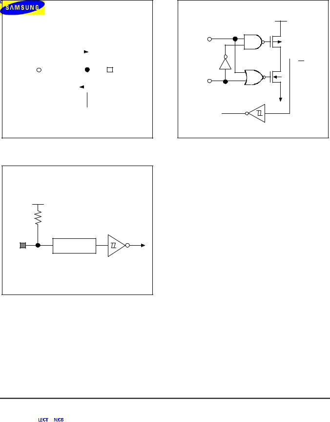
Figure 1-4. Pin Circuit Type A |
Figure 1-6. Pin Circuit Type D-1 |
VDD |
280 KΩ |
Noise Filter |
RESET |
Figure 1-5. Pin Circuit Type B (RESET) |
1-7
PRODUCT OVERVIEW |
KS88C6216/C6224/C6232/P6232 |
|
|
VDD
Typical
47-KΩ
Pull-up Enable 
VDD
Data 

 Output
Open drain
Output Disable
VSS
Input
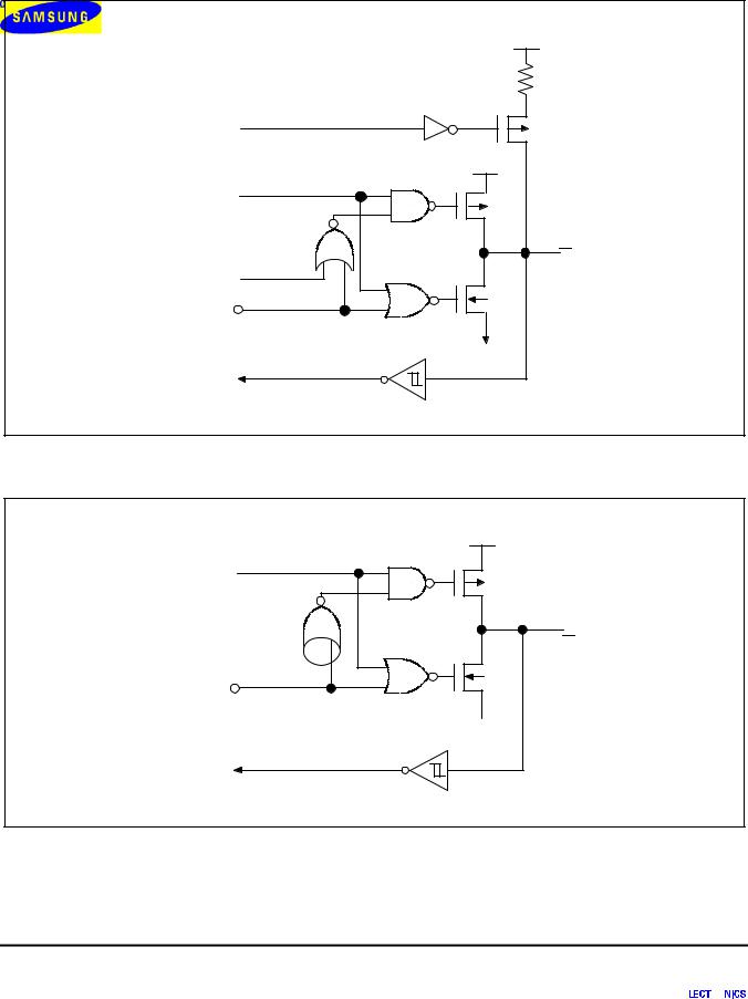
Figure 1-7. Pin Circuit Type E
VDD
Data 

 Output
Open drain 

Output Disable
VSS 
Input
Figure 1-8. Pin Circuit Type E-1
1-8
 Loading...