Motorola C106D, C106B, C106F, C106A Datasheet

MOTOROLA
SEMICONDUCTOR TECHNICAL DATA
Order this document by C106/D
Silicon Controlled Rectifier
Reverse Blocking Triode Thyristors
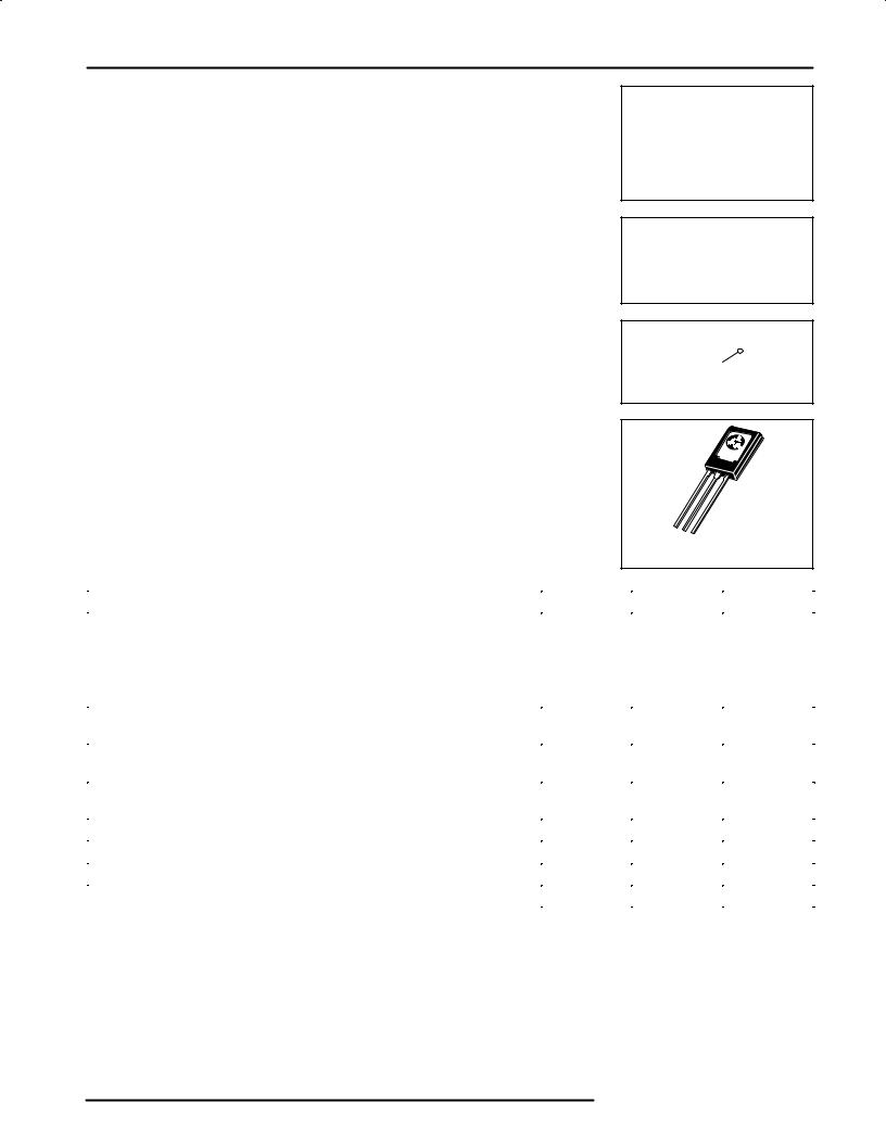
. . . Glassivated PNPN devices designed for high volume consumer applications such as temperature, light, and speed control; process and remote control, and warning systems where reliability of operation is important.
•Glassivated Surface for Reliability and Uniformity
•Power Rated at Economical Prices
•Practical Level Triggering and Holding Characteristics
•Flat, Rugged, Thermopad Construction for Low Thermal Resistance, High Heat Dissipation and Durability
MAXIMUM RATINGS (TJ = 25°C unless otherwise noted.)
C106
Series*
*Motorola preferred devices
SCRs
4 AMPERES RMS
50 thru 600 VOLTS
G
A 

 K
K
G |
CASE 77-08 |
(TO-225AA) |
|
A K |
STYLE 2 |
Rating |
|
Symbol |
Value |
Unit |
|
|
|
|
|
Peak Repetitive Forward and Reverse Blocking Voltage(1) |
V |
|
Volts |
|
(RGK = 1 kΩ) |
|
DRM |
|
|
C106F |
or |
50 |
|
|
(TC = ±40° to 110°C) |
C106A |
VRRM |
100 |
|
|
C106B |
|
200 |
|
|
C106D |
|
400 |
|
|
C106M |
|
600 |
|
|
|
|
|
|
RMS Forward Current |
|
IT(RMS) |
4 |
Amps |
(All Conduction Angles) |
|
|
|
|
|
|
|
|
|
Average Forward Current |
|
IT(AV) |
2.55 |
Amps |
(TA = 30°C) |
|
|
|
|
Peak Non-repetitive Surge Current |
|
ITSM |
20 |
Amps |
(1/2 Cycle, 60 Hz, TJ = ±40 to +110°C) |
|
|
|
|
Circuit Fusing (t = 8.3 ms) |
|
I2t |
1.65 |
A2s |
Peak Gate Power |
|
PGM |
0.5 |
Watt |
Average Gate Power |
|
PG(AV) |
0.1 |
Watt |
Peak Forward Gate Current |
|
IGFM |
0.2 |
Amp |
1. VDRM and VRRM for all types can be applied on a continuous basis. Ratings apply for zero or negative gate voltage; however, (cont.) positive gate voltage shall not be applied concurrent with negative potential on the anode. Blocking voltages shall not be tested with a constant current source such that the voltage ratings of the devices are exceeded.
Preferred devices are Motorola recommended choices for future use and best overall value.
Motorola, Inc. 1995

C106 Series
MAXIMUM RATINGS Ð continued
Rating |
Symbol |
Value |
Unit |
|
|
|
|
Peak Reverse Gate Voltage |
VGRM |
6 |
Volts |
Operating Junction Temperature Range |
TJ |
±40 to +110 |
°C |
Storage Temperature Range |
Tstg |
±40 to +150 |
°C |
Mounting Torque(1) |
Ð |
6 |
in. lb. |
1.Torque rating applies with use of compression washer (B52200F006). Mounting torque in excess of 6 in. lb. does not appreciably lower
case-to-sink thermal resistance. Anode lead and heatsink contact pad are common.
For soldering purposes (either terminal connection or device mounting), soldering temperatures shall not exceed +200°C. For optimum results, an activated flux (oxide removing) is recommended.
THERMAL CHARACTERISTICS (TC = 25°C, RGK = 1 kΩ unless otherwise noted.)
Characteristic |
|
|
|
Symbol |
|
|
Max |
|
|
Unit |
||
|
|
|
|
|
|
|
|
|
|
|
|
|
Thermal Resistance, Junction to Case |
|
|
|
RθJC |
|
|
3 |
|
|
°C/W |
||
Thermal Resistance, Junction to Ambient |
|
|
|
RθJA |
|
|
75 |
|
|
°C/W |
||
ELECTRICAL CHARACTERISTICS (TC = 25°C unless otherwise noted.) |
|
|
|
|
|
|
|
|
|
|
||
Characteristic |
|
|
Symbol |
|
Min |
Typ |
Max |
|
Unit |
|||
|
|
|
|
|
|
|
|
|
|
|
|
|
Peak Forward or Reverse Blocking Current |
TJ = 25°C |
|
IDRM, IRRM |
|
Ð |
|
Ð |
10 |
|
μA |
||
(VAK = Rated VDRM or VRRM, RGK = 1000 Ohms) |
|
|
|
|
|
|
||||||
|
TJ = 110°C |
|
|
|
|
Ð |
|
Ð |
100 |
|
μA |
|
Forward ªOnº Voltage |
|
|
VTM |
|
Ð |
|
Ð |
2.2 |
|
Volts |
||
(IFM = 1 A Peak) |
|
|
|
|
|
|
|
|
|
|
|
|
Gate Trigger Current (Continuous dc) |
|
|
IGT |
|
Ð |
|
30 |
200 |
|
μA |
||
(VAK = 6 Vdc, RL = 100 Ohms) |
|
|
|
|
|
|
|
|
||||
(VAK = 6 Vdc, RL = 100 Ohms, TC = ±40°C) |
|
|
|
|
|
Ð |
|
75 |
500 |
|
|
|
Gate Trigger Voltage (Continuous dc) |
TJ = 25°C |
|
VGT |
|
0.4 |
|
Ð |
0.8 |
|
Volts |
||
(VAK = 6 Vdc, RL = 100 Ohms, RGK = 1000 Ohms) |
|
|
|
|
|
|
|
|||||
(VAK = Rated VDRM, RL = 3000 Ohms, |
|
|
|
|
|
0.5 |
|
Ð |
1 |
|
|
|
RGK = 1000 Ohms, TJ = 110°C) |
TJ = ±40°C |
|
|
|
|
0.2 |
|
Ð |
Ð |
|
|
|
Holding Current |
TJ = 25°C |
|
IHX |
|
0.3 |
|
Ð |
3 |
|
mA |
||
(VD = 12 Vdc, RGK = 1000 Ohms) |
TJ = ±40°C |
|
|
|
|
0.4 |
|
Ð |
6 |
|
|
|
|
TJ = +110°C |
|
|
|
|
0.14 |
Ð |
2 |
|
|
||
Forward Voltage Application Rate |
|
|
dv/dt |
|
Ð |
|
8 |
Ð |
|
V/μs |
||
(TJ = 110°C, RGK = 1000 Ohms, VD = Rated VDRM) |
|
|
|
|
|
|
|
|
|
|
|
|
Turn-On Time |
|
|
tgt |
|
Ð |
|
1.2 |
Ð |
|
μs |
||
Turn-Off Time |
|
|
tq |
|
Ð |
|
40 |
Ð |
|
μs |
||
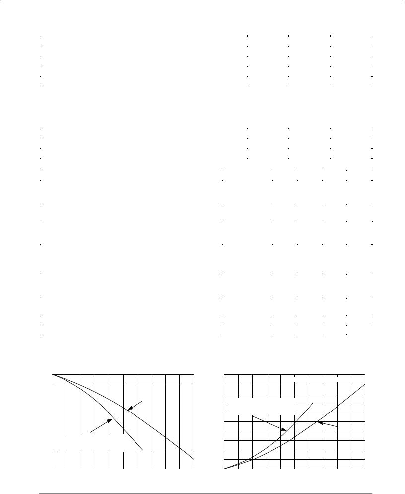
TC, CASE TEMPERATURE (°C)
FIGURE 1 ± AVERAGE CURRENT DERATING
110
100
90 |
|
|
|
|
|
|
|
|
|
|
DC |
||
80 |
|
|
|
|
||
|
|
|
|
|
|
|
|
|
|
|
|
|
|
70 |
|
|
|
|
|
|
|
|
|
|
|
|
|
60 |
|
|
|
|
|
|
|
|
|
|
|
|
|
50 |
|
|
|
|
|
|
|
HALF SINE WAVE |
|
||||
40 |
|
|||||
|
RESISTIVE OR INDUCTIVE LOAD. |
|||||
|
|
|||||
30 |
|
50 to 400 Hz |
|
|
|
|
20 |
|
|
|
|
|
|
|
|
|
|
|
|
|
10 |
|
|
|
|
|
|
0 |
.4 |
.8 |
1.2 1.6 2.0 2.4 2.8 3.2 3.6 4.0 |
|||
IT(AV) AVERAGE ON-STATE CURRENT (AMPERES)
P(AV), AVERAGE ON-STATE POWER DISSIPATION (WATTS)
FIGURE 2 ± MAXIMUM ON-STATE POWER DISSIPATION
10
JUNCTION TEMPERATURE ≈ 110°C
8
HALF SINE WAVE
RESISTIVE OR INDUCTIVE LOAD
6 50 TO 400Hz.
DC
4
2
0
0 |
.4 |
.8 |
1.2 |
1.6 |
2.0 |
2.4 |
2.6 |
3.2 |
3.6 |
4.0 |
IT(AV) AVERAGE ON-STATE CURRENT (AMPERES)
2 |
Motorola Thyristor Device Data |
 Loading...