


September 1986
Revised February 2000
DM74ALS86
Quad 2-Input Exclusive-OR Gate
General Description
This device contains four independent gates, each of which performs the logic exclusive-OR function.
Features
■Switching specifications at 50 pF
■Switching specifications guaranteed over full temperature and VCC range
■Advanced oxide-isolated, ion-implanted Schottky TTL process
■Functionally and pin for pin compatible with Schottky and low power Schottky TTL counterpart
■Improved AC performance over Schottky and low power Schottky counterparts
Ordering Code:
Order Number |
Package Number |
Package Description |
|
|
|
DM74ALS86M |
M14A |
14-Lead Small Outline Integrated Circuit (SOIC), JEDEC MS-012, 0.150 Narrow |
|
|
|
DM74ALS86N |
N14A |
14-Lead Plastic Dual-In-Line Package (PDIP), JEDEC MS-001, 0.300 Wide |
|
|
|
Devices also available in Tape and Reel. Specify by appending the suffix letter “X” to the ordering code.
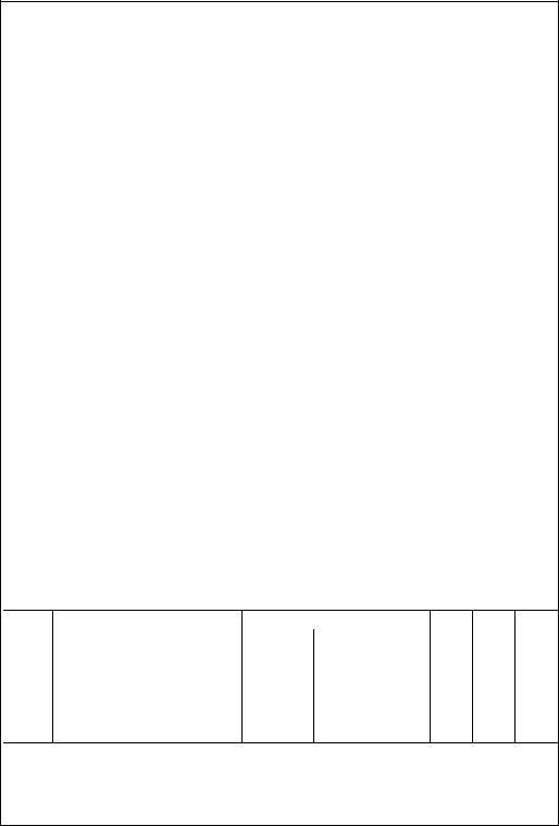
Connection Diagram |
Function Table |
|
|
|
|
||||
|
|
|
Y = A Å B = |
A |
B + AB |
|
|||
|
|
|
|
|
|
|
|||
|
|
|
Inputs |
|
Output |
||||
|
|
|
|
|
|
|
|||
|
|
A |
|
B |
|
Y |
|||
|
|
|
|
|
|
|
|||
|
|
L |
|
L |
|
L |
|||
|
|
L |
|
H |
|
H |
|||
|
|
H |
|
L |
|
H |
|||
|
|
H |
|
H |
|
L |
|||
|
|
|
|
|
|
|
|
|
|
H = HIGH Logic Level
L = LOW Logic Level
Gate OR-Exclusive Input-2 Quad DM74ALS86
© 2000 Fairchild Semiconductor Corporation |
DS006195 |
www.fairchildsemi.com |
DM74ALS86
Absolute Maximum Ratings(Note 1)
Supply Voltage |
7V |
Input Voltage |
7V |
Operating Free Air Temperature Range |
0°C to +70°C |
Storage Temperature Range |
−65°C to +150°C |
Typical θJA |
|
N Package |
87.0°C/W |
M Package |
117.2°C/W |
Note 1: The “Absolute Maximum Ratings” are those values beyond which the safety of the device cannot be guaranteed. The device should not be operated at these limits. The parametric values defined in the Electrical Characteristics tables are not guaranteed at the absolute maximum ratings. The “Recommended Operating Conditions” table will define the conditions for actual device operation.
Recommended Operating Conditions
Symbol |
Parameter |
Min |
Nom |
Max |
Units |
|
|
|
|
|
|
VCC |
Supply Voltage |
4.5 |
5 |
5.5 |
V |
VIH |
HIGH Level Input Voltage |
2 |
|
|
V |
VIL |
LOW Level Input Voltage |
|
|
0.8 |
V |
IOH |
HIGH Level Output Current |
|
|
−0.4 |
mA |
IOL |
LOW Level Output Current |
|
|
8 |
mA |
TA |
Free Air Operating Temperature |
0 |
|
70 |
°C |
Electrical Characteristics
over recommended operating free air temperature range. All typical values are measured at VCC = 5V, TA = 25°C.
Symbol |
Parameter |
Conditions |
|
Min |
Typ |
Max |
Units |
|
|
|
|
|
|
|
|
VIK |
Input Clamp Voltage |
VCC = 4.5V, II = −18 mA |
|
|
|
−1.5 |
V |
VOH |
HIGH Level |
IOH = −0.4 mA |
|
VCC − 2 |
|
|
V |
|
Output Voltage |
VCC = 4.5V to 5.5V |
|
|
|
||
|
|
|
|
|
|
||
VOL |
LOW Level |
VCC = 4.5V |
IOL = 4 mA |
|
0.25 |
0.4 |
V |
|
Output Voltage |
|
IOL = 8 mA |
|
0.35 |
0.5 |
V |
II |
Input Current @ Maximum |
VCC = 5.5V, VIH = 7V |
|
|
|
0.1 |
mA |
|
Input Voltage |
|
|
|
|||
|
|
|
|
|
|
|
|
|
|
|
|
|
|
|
|
IIH |
HIGH Level Input Current |
VCC = 5.5V, VIH = 2.7V |
|
|
|
20 |
μA |
IIL |
LOW Level Input Current |
VCC = 5.5V, VIL = 0.4V |
|
|
|
−0.1 |
mA |
IO |
Output Drive Current |
VCC = 5.5V |
VO = 2.25V |
−30 |
|
−112 |
mA |
ICCL |
Supply Current with |
VCC = Max, All Inputs at 4.5V |
|
|
3.9 |
5.9 |
mA |
|
Outputs LOW |
|
|
||||
|
|
|
|
|
|
|
|
|
|
|
|
|
|
|
|
ICCH |
Supply Current with |
VCC = Max, A Inputs at 0.0V |
|
|
3.8 |
4.5 |
mA |
|
Outputs HIGH |
B Inputs at 4.5V |
|
|
|||
|
|
|
|
|
|
||
|
|
|
|
|
|
|
|
Switching Characteristics
over recommended operating free air temperature range.
Symbol |
Parameter |
|
Conditions |
Min |
Max |
Units |
|
|
|
|
|
|
|
tPLH |
Propagation Delay Time |
(Note 2) |
A or B to Y |
3 |
17 |
ns |
|
LOW-to-HIGH Level Output |
|
Other Input LOW |
|||
|
|
|
|
|
||
|
|
|
|
|
|
|
tPHL |
Propagation Delay Time |
|
|
2 |
12 |
ns |
|
HIGH-to-LOW Level Output |
|
|
|||
|
|
|
|
|
|
|
|
|
|
|
|
|
|
tPLH |
Propagation Delay Time |
|
A or B to Y |
2 |
17 |
ns |
|
LOW-to-HIGH Level Output |
|
Other Input HIGH |
|||
|
|
|
|
|
||
|
|
|
|
|
|
|
tPHL |
Propagation Delay Time |
|
|
2 |
10 |
ns |
|
HIGH-to-LOW Level Output |
|
|
|||
|
|
|
|
|
|
Note 2: VCC = 4.5V to 5.5V, RL = 500Ω, CL = 50 pF.
www.fairchildsemi.com |
2 |
 Loading...