


SGS Thomson Microelectronics TSL062ID, TS062ACD, TL062M, TL062IN, TL062I Datasheet
...TL062
TL062A - TL062B
LOW POWER J-FET DUAL OPERATIONAL AMPLIFIERS
■VERY LOW POWER CONSUMPTION : 200μA
■WIDE COMMON-MODE (UP TO VCC+) AND DIFFERENTIAL VOLTAGE RANGES
■LOW INPUT BIAS AND OFFSET CURRENTS
■OUTPUT SHORT-CIRCUIT PROTECTION
■HIGH INPUT IMPEDANCE J-FET INPUT STAGE
■INTERNAL FREQUENCY COMPENSATION
■LATCH UP FREE OPERATION
■HIGH SLEW RATE : 3.5V/μs
DESCRIPTION
The TL062, TL062A and TL062B are high speed J-FET input dual operational amplifier family. Each of these J-FET input operational amplifiers incorporates well matched, high voltage J-FET and bipolar transistors in a monolithic integrated circuit. The devices feature high slew rates, low input bias and offsetcurrents, andlow offset voltage temperature coefficient.
PIN CONNECTIONS (top view)
1 |
|
|
2 |
- |
|
3 |
+ |
- |
|
||
4 |
|
+ |
N |
D |
DIP8 |
SO8 |
(Plastic Package) |
(Plastic Micropackage) |
ORDER CODES
Part Number |
Temperature Range |
Package |
||
N |
D |
|||
|
|
|||
TL062M/AM/BM |
-55oC, +125oC |
● |
● |
|
TL062I/AI/BI |
-40oC, +105oC |
● |
● |
|
TL062C/AC/BC |
0oC, +70oC |
● |
● |
|
Example : TL062IN
8
1 - Output 1
2 - Inverting input 1
73 - Non-inverting input 1
4 - VCC-
6
5 - Non-inverting input 2
6 - Inverting input 2
7 - Output 2
5 8 - VCC+
October 1997 |
1/10 |
TL062 - TL062A - TL062B
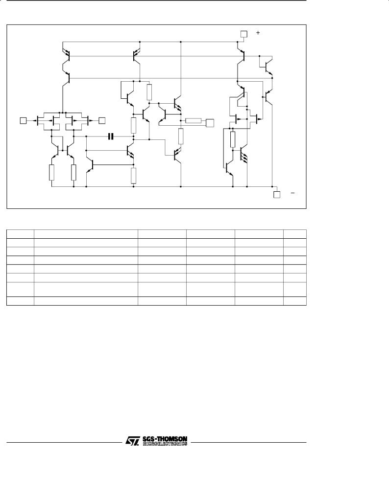
SCHEMATIC DIAGRAM
VC C
|
220 Ω |
|
|
|
Inverting |
Non-inverting |
|
|
|
Input |
Input |
Ω |
Output |
1/2 TL062 |
|
64 |
|
||
|
45k Ω |
|
|
|
270 Ω |
Ω |
3.2k |
4.2k Ω |
Ω |
100 |
V CC
MAXIMUM RATINGS
Symbol |
Parameter |
TL062M,AM,BM |
TL062I,AI,BI |
TL062C,AC,BC |
Unit |
VCC |
Supply Voltage - (note 1) |
±18 |
±18 |
±18 |
V |
Vi |
Input Voltage - (note 3) |
±15 |
±15 |
±15 |
V |
Vid |
Differential Input Voltage - (note 2) |
±30 |
±30 |
±30 |
V |
Ptot |
Power Dissipation |
680 |
680 |
680 |
mW |
|
Output Short-Circuit Duration (Note 4) |
Infinite |
Infinite |
Infinite |
|
Toper |
Operating Free-Air Temperature |
-55 to +125 |
-40 to +105 |
0 to +70 |
oC |
|
Range |
|
|
|
|
Tstg |
Storage Temperature Range |
- 65 to + 150 |
- 65 to + 150 |
- 65 to + 150 |
oC |
Notes : 1. All voltage values, except differential voltage, are with respect to the zero reference level (ground) of the supply voltages where the zero reference level is the midpoint between VCC+ and VCC-.
2.Differential voltages are at the non-inverting input terminal with respect to the inverting input terminal.
3.The magnitude of the input voltage must never exceed the magnitude of the supply voltage or 15 volts, whichever is less.
4.The output may be shorted to ground or to either supply. Temperature and/or supply voltages must be limited to ensure that the dissipation rating is not exceeded.
2/10

|
|
|
|
|
|
|
|
TL062 - TL062A - TL062B |
|||||
ELECTRICAL CHARACTERISTICS |
|
|
|
|
|
|
|
|
|
|
|||
VCC = ± 15V, Tamb = 25oC (unless otherwise specified) |
|
|
|
|
|
|
|
||||||
Symbol |
Parameter |
TL062M |
|
|
TL062I |
|
|
TL062C |
|
Unit |
|||
Min. Typ. Max. Min. Typ. Max. Min. Typ. Max. |
|||||||||||||
|
|
|
|
||||||||||
Vio |
Input Offset Voltage (Rs = 50Ω) |
|
|
|
|
|
|
|
|
|
mV |
||
|
Tamb |
= 25oC |
|
3 |
6 |
|
3 |
6 |
|
3 |
15 |
|
|
|
Tmin. |
≤ Tamb ≤ Tmax. |
|
|
15 |
|
|
9 |
|
|
20 |
|
|
DVio |
Temperature Coefficient of Input |
|
|
|
|
|
|
|
|
|
μV/oC |
||
|
Offset Voltage (Rs = 50Ω) |
|
10 |
|
|
10 |
|
|
10 |
|
|
||
Iio |
Input Offset Current * |
|
|
|
|
|
|
|
|
|
|
||
|
Tamb |
= 25oC |
|
5 |
100 |
|
5 |
100 |
|
5 |
200 |
pA |
|
|
Tmin. |
≤ Tamb ≤ Tmax. |
|
|
20 |
|
|
10 |
|
|
5 |
nA |
|
Iib |
Input Bias Current * |
|
|
|
|
|
|
|
|
|
|
||
|
Tamb |
= 25oC |
|
30 |
200 |
|
30 |
200 |
|
30 |
400 |
pA |
|
|
Tmin. ≤ Tamb ≤ Tmax. |
|
|
50 |
|
|
20 |
|
|
10 |
nA |
||
Vicm |
Input Common Mode Voltage |
±11.5 |
+15 |
|
±11.5 |
+15 |
|
±11 |
+15 |
|
V |
||
|
Range |
|
|
-12 |
|
|
-12 |
|
|
-12 |
|
|
|
VOPP |
Output Voltage Swing (RL = 10kΩ) |
|
|
|
|
|
|
|
|
|
V |
||
|
Tamb |
= 25oC |
20 |
27 |
|
20 |
27 |
|
20 |
27 |
|
|
|
|
Tmin. |
≤ Tamb ≤ Tmax. |
20 |
|
|
20 |
|
|
20 |
|
|
|
|
Avd |
Large Signal Voltage Gain |
|
|
|
|
|
|
|
|
|
V/mV |
||
|
(RL = 10kΩ, Vo = ± 10V) |
|
|
|
|
|
|
|
|
|
|
||
|
Tamb |
= 25oC |
4 |
6 |
|
4 |
6 |
|
3 |
6 |
|
|
|
|
Tmin. |
≤ Tamb ≤ Tmax. |
4 |
|
|
4 |
|
|
3 |
|
|
|
|
GBP |
Gain Bandwidth Product |
|
|
|
|
|
|
|
|
|
MHz |
||
|
(Tamb = 25oC, RL = 10kΩ |
|
|
|
|
|
|
|
|
|
|
||
|
CL = 100pF) |
|
|
1 |
|
|
1 |
|
|
1 |
|
|
|
Ri |
Input Resistance |
|
1012 |
|
|
1012 |
|
|
1012 |
|
Ω |
||
CMR |
Common Mode Rejection Ratio |
|
|
|
|
|
|
|
|
|
dB |
||
|
(Rs = 50Ω) |
|
80 |
86 |
|
80 |
86 |
|
70 |
76 |
|
|
|
SVR |
Supply Voltage Rejection Ratio |
|
|
|
|
|
|
|
|
|
dB |
||
|
(Rs = 50Ω) |
|
80 |
95 |
|
80 |
95 |
|
70 |
95 |
|
|
|
Icc |
Supply Current (Per Amplifier) |
|
|
|
|
|
|
|
|
|
μA |
||
|
(Tamb = 25oC, no load, no signal) |
|
200 |
250 |
|
200 |
250 |
|
200 |
250 |
|
||
VO1/VO2 |
Channel Separation |
|
|
|
|
|
|
|
|
|
dB |
||
|
(Av = 100, Tamb = 25oC) |
|
120 |
|
|
120 |
|
|
120 |
|
|
||
PD |
Total Power Consumption |
|
|
|
|
|
|
|
|
|
mW |
||
|
(Each Amplifier) |
|
|
|
|
|
|
|
|
|
|
|
|
|
(Tamb = 25oC, no load, no signal) |
|
6 |
7.5 |
|
6 |
7.5 |
|
6 |
7.5 |
|
||
*Input bias currents of a FET-input operational amplifier are normal junction reverse currents, which are temperature sensitive. Pulse techniques must be used that will maintain the junction temperature as closes to the ambient temperature as possible.
ELECTRICAL CHARACTERISTICS (continued)
VCC = ± 15V, Tamb = 25oC
Symbol |
Parameter |
|
TL062C,I,M |
Unit |
|
Min. |
Typ. |
||||
|
|
Max. |
|||
SR |
Slew Rate (Vi = 10V, RL = 10kΩ, CL = 100pF, AV = 1) |
1.5 |
3.5 |
V/μs |
|
tr |
Rise Time (Vi = 20mV, RL = 10kΩ, CL = 100pF, AV = 1) |
|
0.2 |
μs |
|
KOV |
Overshoot Factor (Vi = 20mV, RL = 10kΩ, CL = 100pF, AV = 1) |
|
|
% |
|
|
(see figure 1) |
|
10 |
|
|
en |
Equivalent Input Noise Voltage |
|
|
nV |
|
|
(Rs = 100Ω, f = 1KHz) |
|
42 |
```√ Hz |
3/10
 Loading...