


MOTOROLA SN74LS74AM, SN74LS74AMEL, SN74LS74AML1, SN74LS74AML2, SN74LS74AMR1 Datasheet
...
SN74LS74A
Dual D-Type Positive
Edge-Triggered Flip-Flop
The SN74LS74A dual edge-triggered flip-flop utilizes Schottky TTL circuitry to produce high speed D-type flip-flops. Each flip-flop has individual clear and set inputs, and also complementary Q and Q outputs.
Information at input D is transferred to the Q output on the positive-going edge of the clock pulse. Clock triggering occurs at a voltage level of the clock pulse and is not directly related to the transition time of the positive-going pulse. When the clock input is at either the HIGH or the LOW level, the D input signal has no effect.
MODE SELECT ± TRUTH TABLE
OPERATING MODE |
|
|
|
INPUTS |
|
|
|
OUTPUTS |
|||||||
|
|
|
|
|
|
|
|
|
|
|
|
|
|
|
|
|
|
|
|
|
|
|
|
|
|
D |
Q |
|
|
|
|
|
|
SD |
|
|
SD |
|
|
|
|
Q |
|
||||
Set |
|
L |
|
|
|
H |
|
|
X |
H |
|
L |
|||
Reset (Clear) |
|
H |
|
|
|
L |
|
|
X |
L |
|
H |
|||
*Undetermined |
|
L |
|
|
|
L |
|
|
X |
H |
|
H |
|||
Load ª1º (Set) |
|
H |
|
|
|
H |
|
|
h |
H |
|
L |
|||
Load ª0º (Reset) |
|
H |
|
|
|
H |
|
|
l |
L |
|
H |
|||
|
|
|
|
|
|
|
|
|
|
|
|
|
|
|
|
|
|
|
|
|
|
|
|
|
|
|
|
|
|
|
|
*Both outputs will be HIGH while both SD and CD are LOW, but the output states are unpredictable if SD and CD go HIGH simultaneously. If the levels at the set and clear are near VIL maximum then we cannot guarantee to meet the minimum level for VOH.
H, h = HIGH Voltage Level
L, I = LOW Voltage Level
X = Don't Care
l, h (q) = Lower case letters indicate the state of the referenced input
(or output) one set-up time prior to the HIGH to LOW clock transition.
GUARANTEED OPERATING RANGES
Symbol |
Parameter |
Min |
Typ |
Max |
Unit |
|
|
|
|
|
|
VCC |
Supply Voltage |
4.75 |
5.0 |
5.25 |
V |
TA |
Operating Ambient |
0 |
25 |
70 |
°C |
|
Temperature Range |
|
|
|
|
|
|
|
|
|
|
IOH |
Output Current ± High |
|
|
± 0.4 |
mA |
IOL |
Output Current ± Low |
|
|
8.0 |
mA |
http://onsemi.com
LOW
POWER
SCHOTTKY
14 
1
PLASTIC
N SUFFIX
CASE 646
14
1
SOIC
D SUFFIX
CASE 751A
ORDERING INFORMATION
Device |
Package |
Shipping |
|
|
|
SN74LS74AN |
14 Pin DIP |
2000 Units/Box |
|
|
|
SN74LS74AD |
14 Pin |
2500/Tape & Reel |
|
|
|
Semiconductor Components Industries, LLC, 1999 |
1 |
Publication Order Number: |
December, 1999 ± Rev. 6 |
|
SN74LS74A/D |
SN74LS74A
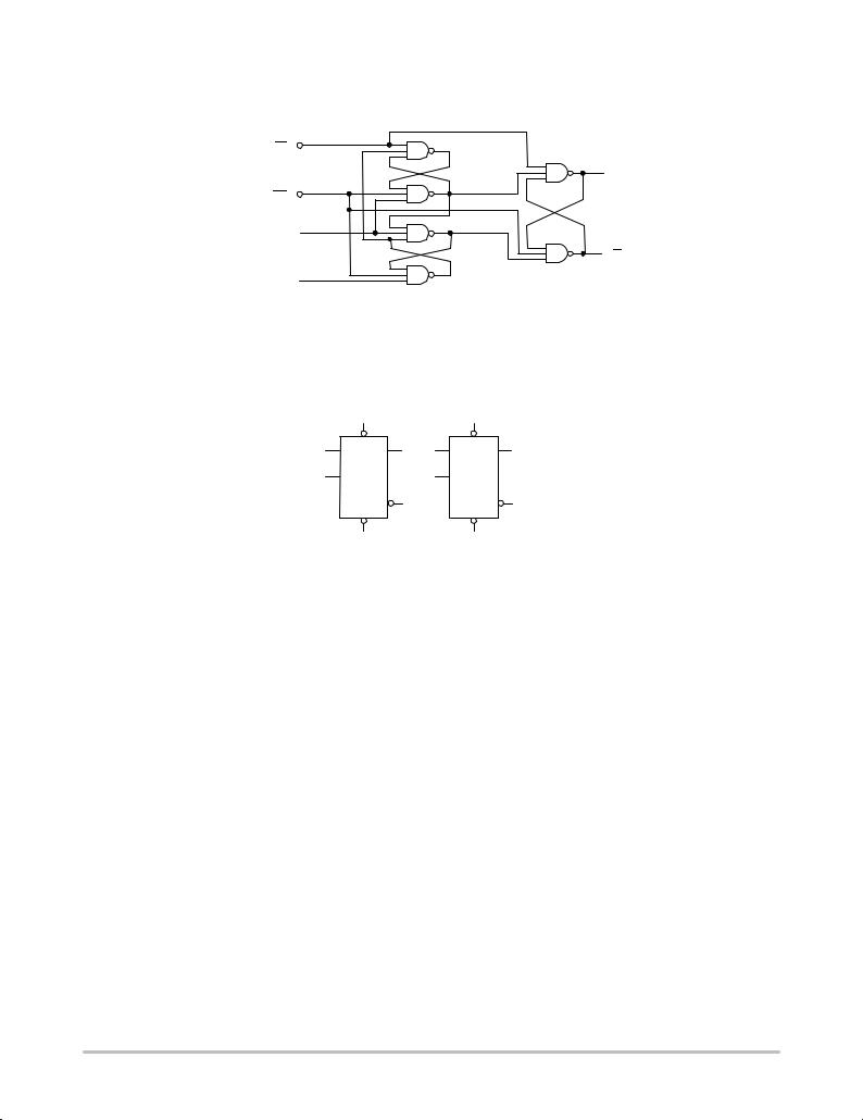
LOGIC DIAGRAM (Each Flip-Flop)
SET (SD)4 (10)
 Q 5 (9)
CLEAR (CD)
1 (13)
CLOCK  3 (11)
 Q 6 (8)
D 
2 (12)
LOGIC SYMBOL
|
4 |
|
|
10 |
|
2 |
D SD Q |
5 |
12 |
D SD Q |
9 |
3 |
CP |
|
11 |
CP |
|
|
Q |
6 |
|
Q |
8 |
|
CD |
|
|
CD |
|
|
1 |
|
|
13 |
|
|
|
VCC = PIN 14 |
|
|
|
|
|
GND = PIN 7 |
|
|
|
http://onsemi.com
2
SN74LS74A
DC CHARACTERISTICS OVER OPERATING TEMPERATURE RANGE (unless otherwise specified)
|
|
|
Limits |
|
|
|
|
|
|
|
|
|
|
|
|
Symbol |
Parameter |
Min |
Typ |
Max |
Unit |
Test Conditions |
|
|
|
|
|
|
|
|
|
VIH |
Input HIGH Voltage |
2.0 |
|
|
V |
Guaranteed Input HIGH Voltage for |
|
|
|
All Inputs |
|
||||
VIL |
Input LOW Voltage |
|
|
0.8 |
V |
Guaranteed Input LOW Voltage for |
|
|
|
|
All Inputs |
|
|||
VIK |
Input Clamp Diode Voltage |
|
± 0.65 |
± 1.5 |
V |
VCC = MIN, IIN = ± 18 mA |
|
VOH |
Output HIGH Voltage |
2.7 |
3.5 |
|
V |
VCC = MIN, IOH = MAX, VIN = VIH |
|
|
|
|
|
or VIL per Truth Table |
|||
|
|
|
|
|
|
||
|
|
|
0.25 |
0.4 |
V |
I = 4.0 mA |
VCC = VCC MIN, |
VOL |
Output LOW Voltage |
|
|
|
|
OL |
VIN = VIL or VIH |
|
0.35 |
0.5 |
V |
IOL = 8.0 mA |
|||
|
|
|
per Truth Table |
||||
|
|
|
|
|
|
|
|
|
Input High Current |
|
|
|
|
|
|
|
Data, Clock |
|
|
20 |
μA |
VCC = MAX, VIN = 2.7 V |
|
IIH |
Set, Clear |
|
|
40 |
|
|
|
|
|
|
|
|
|
|
|
|
Data, Clock |
|
|
0.1 |
mA |
VCC = MAX, VIN = 7.0 V |
|
|
Set, Clear |
|
|
0.2 |
|||
|
|
|
|
|
|
|
|
|
Input LOW Current |
|
|
|
|
|
|
IIL |
Data, Clock |
|
|
± 0.4 |
mA |
VCC = MAX, VIN = 0.4 V |
|
|
Set, Clear |
|
|
± 0.8 |
|
|
|
|
|
|
|
|
|
|
|
IOS |
Output Short Circuit Current (Note 1) |
± 20 |
|
±100 |
mA |
VCC = MAX |
|
ICC |
Power Supply Current |
|
|
8.0 |
mA |
VCC = MAX |
|
Note 1: Not more than one output should be shorted at a time, nor for more than 1 second.
AC CHARACTERISTICS (TA = 25°C, VCC = 5.0 V)
|
|
|
Limits |
|
|
|
|
|
|
|
|
|
|
|
|
Symbol |
Parameter |
Min |
Typ |
Max |
Unit |
Test Conditions |
|
|
|
|
|
|
|
|
|
fMAX |
Maximum Clock Frequency |
25 |
33 |
|
MHz |
Figure 1 |
VCC = 5.0 V |
tPLH |
|
|
13 |
25 |
ns |
|
|
Clock, Clear, Set to Output |
|
Figure 1 |
CL = 15 pF |
||||
|
|
|
|
||||
|
25 |
40 |
ns |
||||
tPHL |
|
|
|
|
|||
AC SETUP REQUIREMENTS (TA = 25°C) |
|
|
|
|
|
|
|
|
|
|
Limits |
|
|
|
|
|
|
|
|
|
|
|
|
Symbol |
Parameter |
Min |
Typ |
Max |
Unit |
Test Conditions |
|
|
|
|
|
|
|
|
|
tW (H) |
Clock |
25 |
|
|
ns |
Figure 1 |
|
tW (L) |
Clear, Set |
25 |
|
|
ns |
Figure 2 |
|
ts |
Data Setup Time Ð HIGH |
20 |
|
|
ns |
Figure 1 |
VCC = 5.0 V |
LOW |
20 |
|
|
ns |
|
||
|
|
|
|
|
|
||
|
|
|
|
|
|
|
|
th |
Hold Time |
5.0 |
|
|
ns |
Figure 1 |
|
http://onsemi.com
3
 Loading...