


IO-A
Table of contents
 Loading...
GE Fanuc Automation
Computer Numerical Control Products
I/O Unit – Model A
Connection / Maintenance Manual
GFZ-61813E/02 April 1992

Warnings, Cautions, and Notes
as Used in this Publication
Warning notices are used in this publication to emphasize that hazardous voltages, currents,
temperatures, or other conditions that could cause personal injury exist in this equipment or
may be associated with its use.
In situations where inattention could cause either personal injury or damage to equipment, a
Warning notice is used.
Caution notices are used where equipment might be damaged if care is not taken.
GFL-001
Warning
Caution
Note
Notes merely call attention to information that is especially significant to understanding and
operating the equipment.
This document is based on information available at the time of its publication. While efforts
have been made to be accurate, the information contained herein does not purport to cover all
details or variations in hardware or software, nor to provide for every possible contingency in
connection with installation, operation, or maintenance. Features may be described herein
which are not present in all hardware and software systems. GE Fanuc Automation assumes
no obligation of notice to holders of this document with respect to changes subsequently made.
GE Fanuc Automation makes no representation or warranty, expressed, implied, or statutory
with respect to, and assumes no responsibility for the accuracy, completeness, sufficiency, or
usefulness of the information contained herein. No warranties of merchantability or fitness for
purpose shall apply.
©Copyright 1992 GE Fanuc Automation North America, Inc.
All Rights Reserved.
Contents
GENERAL
I . CONNECTIONS
l.FANUC I/O Link................................................................ l-l
1.1 Configuration............................................................. l-l
1.2 Allocation of I/O Points................................................. 1-2
2.1/O Unit CONFICURATION........................................................ l-4
3.INSTALLATION
3.1 Environmental Conditions
3.2 Designing Condition for a Cabinet
Outer Dimension of I/O Unit ............................................. 1-6
3.3
3.4 Mounting and Dismounting Modules
4.CONNECTION
4.1 General Connection Diagram
4.2 Connecting Input Power Source
4.3 Grounding
4.4 Connecting Signal Cables
4.5 Connecting with I/O Modules
.................................................................. l-5
................................................. l-5
........................................
.........................................
....................................................................
............................................... l-9
............................................
................................................................
.................................................
..............................................
5.DIGITAL INPUT / OUTPUT MODULES ................................................
5.1 List of Modules
..........................................................
5.2 Correspondence between I/O Signals and Addresses in a Module
5.3 Specification for each Module ............................................
6.ANALOG INPUT MODULE (AADO4A> ..................................................
6.1 Specifications for Analog Input Module
...................................
6.2 Correspondence between Input Signals and Addresses in a Module
6.3 Connecting with Analog Input Module ......................................
7.ANALOG OUTPUT MODULE (ADAOZA)
................................................
7.1 Analog Output Module Specification .......................................
7.2 Correspondence between Output Signals and Addresses in a Module
7.3 Connection to Analog Output Module .......................................
.............
...........
..........
l-5
l-8
l-9
l-10
l-10
1-12
l-15
1-17
l-l?
1-19
1-19
1-48
l-48
l-49
1-51
1-52
l-52
1-53
l-54
c
8.HICH SPEED COUNTER MODULE .....................................................
8.1 Outline of High Speed Counter Module
8.2 Specifications of High Speed Counter Module
....................................
..............................
8.2.1 Pulse counter ........................................................
8.2.2 Comparison function ..................................................
8.2.3 Pulse interface ......................................................
8.2.4 External contact input
8.2.5 External contact output
..............................................
..............................................
8.2.6 Marker processing ....................................................
8.2.7 LED indicators
......................................................
8.3 PMC Interface ............................................................
8.3.1
8.3.2 Mode B
8.3.3 Details of PMC interface signals
Mode A ..............................................................
..............................................................
....................................
8.4 Total Connection of High Speed Counter Module
8.4.1
8.42 Connector signal list
8.5 Connection with Pulse Cenerator
8.5.1 Use of phase A and B pulses
8.5.2 Use of positive/negative pulses
8.6 Connection with Power Magnetics Cabinet
Connection diagram
..................................................
................................................
..........................................
..........................................
......................................
..................................
............................
l-55
l-55
l-57
l-57
1-57
l-59
l-60
1-61
1-61
l-61
l-63
l-63
1-65
l-68
l-69
l-69
l-70
1-71
1-71
1-72
l-73
8.7 I/O Signals Conventions.................................................. l-74
8.?. 1 Solid state relav mtmt sima!s UHJTO tn fHJTi’L= ___= _= = _= _ e_c l-74
8. 7. 2
DC-input signals .(ME and CSP,:. . . .‘_~.-.-..-~. ::,,:I.. . . . . . . . . . . . . . . . . . . .
--- _“_, ..--r-w
9.OPTICAL I/O LINK ADAPTER ...................................................... l-76
9.1 External Dimension of Optical I/O Link
................................... l-76
9.2 Weight of Optical I/O Link ............................................... l-76
9.3 Connection of Optical I/O Link ............................................
9.4 Power Source of Optical I/O Link .........................................
9.5 Installation Conditions of Optical I/O Link
.............................. l-77
9.6 Optical Fiber Cable ......................................................
9.6.1 External view of optical fiber cable .................................
9.6.2 Notice of optical fiber cable handling ............................... l-78
96.3 Optical fiber cable clamping method ..................................
9.6.4 Relay using an optical fiber adapter .................................
9.6.5 Maximum transmission distance by optical fiber cable
................. l-81
II. MAINTENANCE
1 . OVERVIEW ....................................................................
1.1 System Configuration .....................................................
1.2 I/O Unit-A Configuration .................................................
1.3 Block Diagram ............................................................
1.4 List of Units ............................................................
i 75 -_ -
l-76
l-77
l-77
1-78
l-80
l-81
2-l
2-1
2-2
2-3
2-4
2. INDICATION ..................................................................
,
2.1 Interface Module (AIFOIA) LEDs
2.2 Interface Module (AIFOIB) LEDs
...........................................
...........................................
2.3 I/O Module LEDs(Module with 16 or Less I/O Points)
.......................
2-6
2-6
2-9
Z-10
3 . FUSES....................................................................... 2-11
.
4
REMOVING PC BOARDS.......................................................... 2-12
4.1 How To Remove Terminal Board-type I/O Module PC Boards................... 2-12
4.2 How To Remove Interface and Connector-type I/O Module
PC Boards................................................................ 2-14
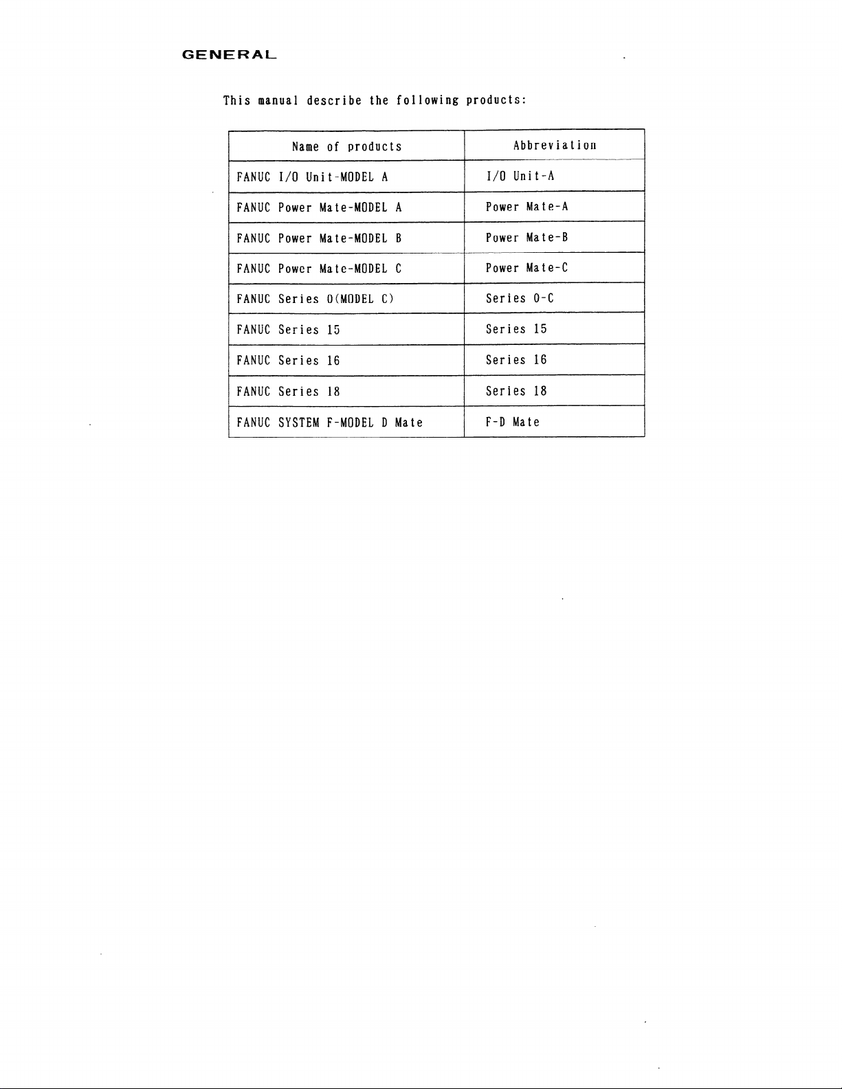
GENERAL
his manual describe the following products:
Name of products
FANUC I/O Unit-MODEL A
FANUC Power Mate-MODEL A
FANUC Power Mate-MODEL B
FANUC Power Mate-MODEL C
Abbreviation
I/O Unit-A
Power Mate-A
Power Mate-B
Power Mate-C
FANUC Series O(MODEL C) Series O-C
FANUC Series 15 Series 15
FANUC Series 16 Series 16
FANUC Series 18 Series 18
FANUC SYSTEM F-MODEL D Mate
F-D Mate

I l CONNECTIONS
FANUC l/O Link
1
l
I/O Link is a serial interface with a purpose to transfer I/O signals (bit data) between
CNC, ccl 1 controller,
at high speed.
1.1 Configuration
the I/O Unit-A, the Power Mate-A, etc.
Master
CNC
F-D Mate -
L--J Y_
- Operator’s
I -
l 0 0
l . l
.
.___._. _ ____ _~._._~_-_.---.----I.----
1
I/O Unit
Slave
I/O Unit
!
LLLLLlLLLLLJLLLLlJ **
.
pane 1
connect ion
Group
#1
unit
A
c
,
_ Power Croup
Mate
#2
.
?
Series Group
o-c
.
#3’
.
_______.___.__________-.~-_.---.-------.-.
I/O Unit
I/O Unit
:
. ,
Group
Croup
#15
I> The FANUC I/O Link is made up of one master and a number of slaves.
Mater : Series O-C, Series 15, Series 16, Series 18, F-D Mate
Slave : I/O Unit-A, Power Mate-A, B, C operator’s panel connection unit,
Series O-C
2) Up to 16 groups of slaves can be connected with a single I/O Link.
Number of slaves per one group is as follows.
I/O Unit-A : Up to 4 units (i. e.4 bases) but when Master is @
Series O-C, Series 15, Series 16 or Series 18 up
to 2 units.
Power Mate-A, B, C
: 1
Operator’s panel connection unit : 1
Ser i es O-C,
: 1
3) Any slave can be connected with any group. However, different types of slaves
can not be connected with a single group.
-1
1
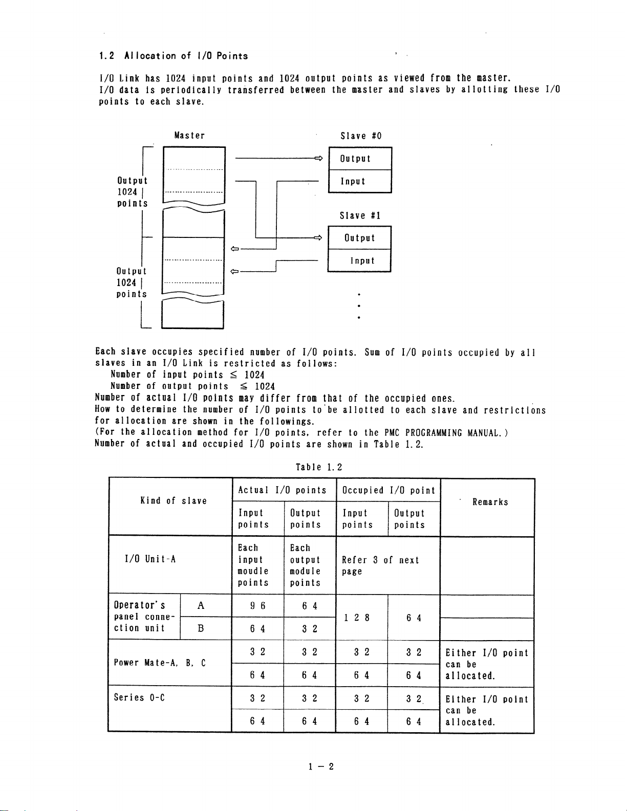
1.2 Allocation of I/O Points
I/O Link has 1024 input points and 1024 output points as viewed from the master.
I/O data is periodically transferred between
points to eal
h slave.
the master and slaves by allotting these I/O
1
Master
Slave 80
r
I
output
1024 1
points
SIave 81
output
1
output
1024 1
points
Input
t
l
0
l
L
Each sIave occupies specified number of I/O points.
slaves in an I/O Link is restricted as follows:
Number of input points I 1024
Number of output points s 1024
Number of actual I/O points may differ from that of the occupied ones.
How to determine the number of I/O points to’be allotted to each slave and restrictions
for allocation are shown in the followings.
(For the allocation method for I/O points, refer to the PMC PROGRAMMING MANUAL.)
Number of actual and occupied I/O points are shown in Table 1.2.
Sum of I/O points occupied by all
Kind of slave
I/O Unit-A
Operator’s
pane I conne-
ction unit
Power Mate-A, B, C
Series O-C
A
B
Table 1.2
Each
input
moudle module
points points
9
6 4 3 2
3
6 4 6 4
3
6
Each
output
6 6 4
2 3 2
2 3 2
4 6 4
Occupied I/O point
e Remarks
Input output
points points
Refer 3 of next
page
1 2 8
3 2 3 2
6 4 6 4
3 2 3 2. Either I/O point
6 4 6 4 al located.
6 4
Either I/O point
can be
7
al located.
can be
\
-2
1
1) Sum the numbers of the occupied I/O points in Table 1 for all slaves connected
with a single I/O Link.
The sum must satisfy the following restriction:
Number of input points 5 1024 (per one I/O Link)
Number of output points I: 1024 (per one I/O Link)
2) Number of the occupied I/O points per one group must satisfy the following
restriction:
Number of input points I: 256 (per one group)
Number of output points 5 256 (per one group?
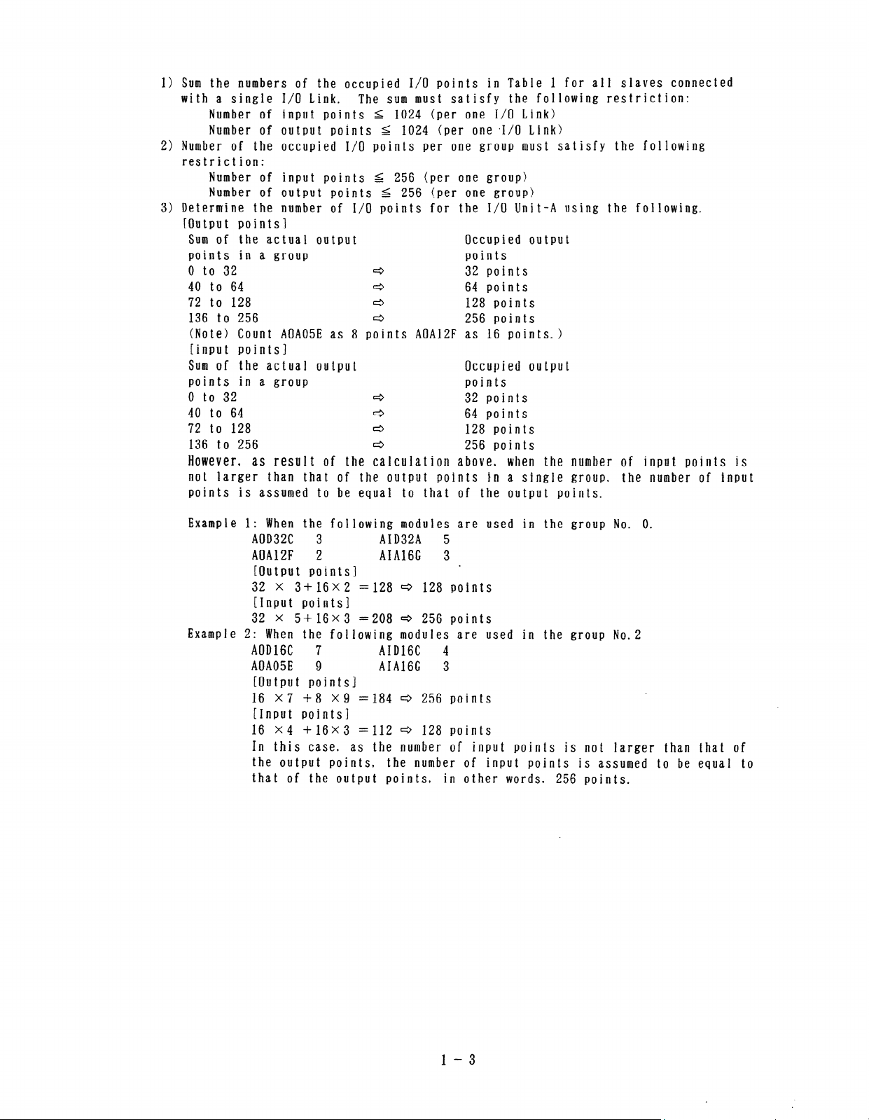
3) Determine the number of I/O points for the I/O Unit-A using the following.
[Output points]
Sum of the actual output
points in a group
0 to 32
40 to 64
72 to 128
136 to 256
c3
r3
c3
4
Occupied output
points
32 points
64 points
128 points
256 points
(Note) Count AOA05E as 8 points AOAIZF as 16 points.)
[input points]
Sum of the actual output
Occupied output
points in a group points
0 to 32
40 to 64
72 to 128
136 to 256
c3
r3
c3
c3
32 points
64 points
128 points
256 points
However, as result of the calculation above. when the number of input points is
not larger than that of the output points in a single group. the number of input
points is assumed to be equal to that of the output points.
Example 1: When the following modules are used in the group No. 0.
AOD32C 3 AID32A 5
AOA12F 2
[Output points]
AIAl6G 3
.
32 x 3+16x2 =I28 c3 128 points
[Input points1
32 x 5+16x3 =208 ~3 256 points
Example 2: When the following modules are used in the group No.2
AODLGC 7 AIDIGC 4
AOA05E 9
AIAlGG 3
[Output points1
16 x7 +8 x9 =184 ~3 256 points
[Input points]
16 x4 +16x3 =112 e3 128 points
In this case. as the number of input points is not larger than that of
the output points, the number of input points is assumed to be equal to
that of the output points,
in other words. 256 points.
-
3
1
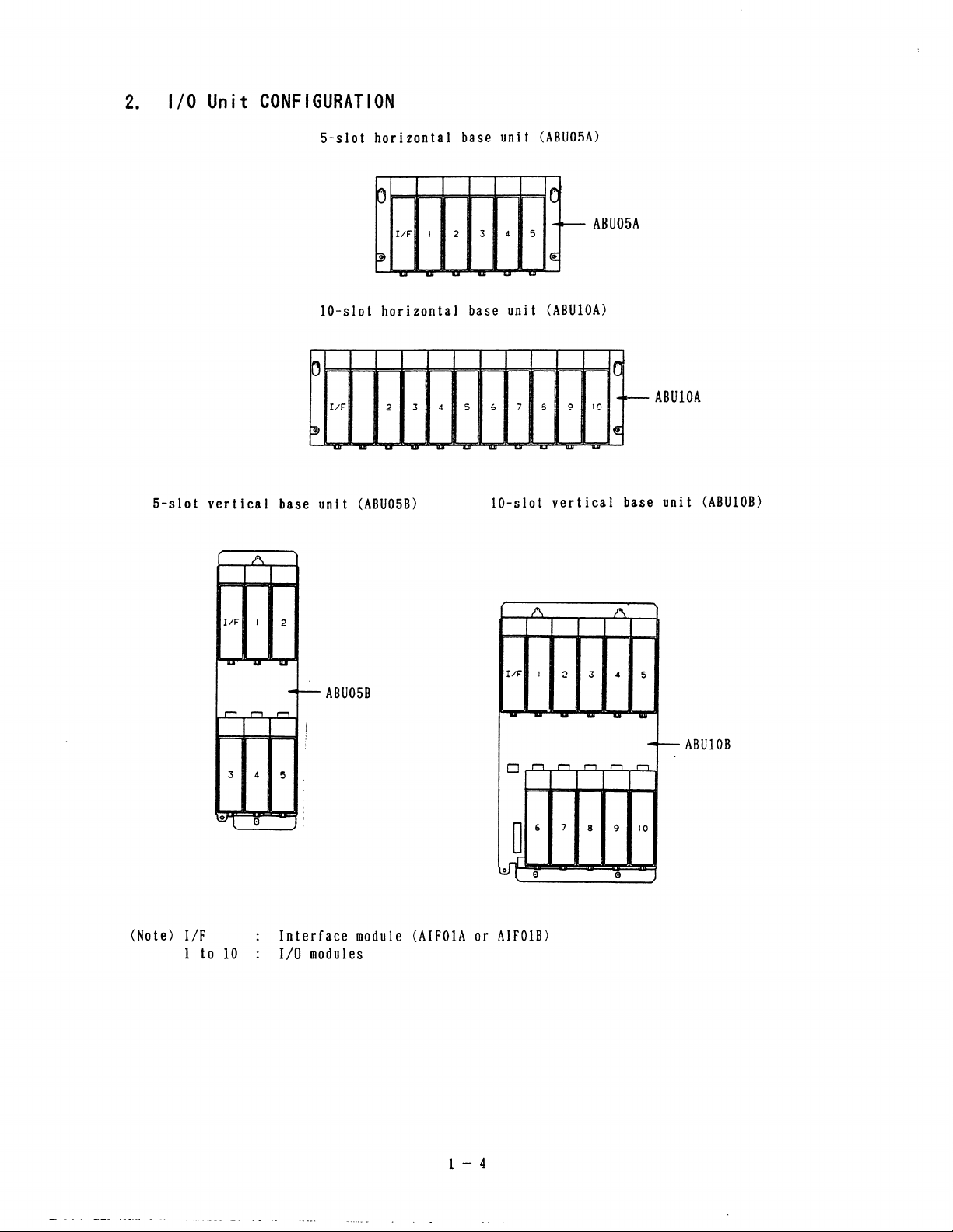
I/O Unit CONFIGURATION
2
.
5-slot horizontal base unit (ABUOSA)
.
6
ABU05A
0
f
lo-slot horizontal base unit (ABUlOA)
ABUlOA
5-slot vertical base unit (ABU05B)
lo-slot vertical base unit (ABUlOB)
- ABU05B
I
(Note) I/F : Interface module (AIFOlA or AIFOlB)
1 to 10 : I/O modules
++--- ABUlOB
_ - - - --.- . --.-- - . . -
-- ._..- . - _ _ - .
__ ._
._ ___
- -. . _ -
. . _
-4
1
_ - _ . .
I~ICI~AI I rrrnmt
IN3 I ALLA I I VI\
3.
3.1 Environmental Conditions
Install the cabinet containing the I/O Unit-A where the following
rnnfiitinnlc arp sstiszfiwi
““..Y. ” * V..” YI ”
“YIIUI *--I
1) Surrounding temperature
During operation: 0 to 45°C
During preservation and transportation: -20 to 60°C
3) Hum’idi ty
Normal condition: 75% or Iess (relative humidity)
Short period (one month or shorter): Max.95%
4) Vibratinn
V”*“..
During operation: 0.5G or less
5) Atmosphere
When the unit is used in areas with high density of dust, cutting fIuid or
organic solvent,the user should consult FANUC.
3.2 Designing Condition for a Cabinet
When designing a cabinet to contain the I/O Unit-A, take the same care as taken for
the cabinet containing the CNC control unit and other units. For details, refer to
the CNC CONNECTING MANUAL.
9Arlitinn urhon
In
uuu 1 L 1 Ullp n11c11
mnwnt i na the I/O ilni t
1IIU u II b 1 116
UIII L, LUlll VI 111 cu
rnnfntm tn the followings in view of
maintenance, environmental durability, noise’resistance and the Iike.
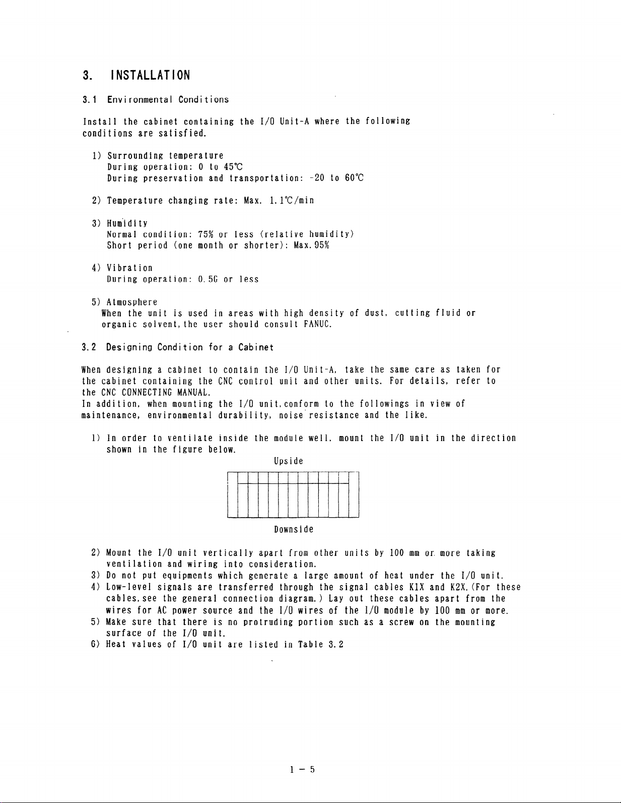
1) In order to ventilate inside the module well, mount the I/O unit in the direction
shown in the figure below.
Upside
Downside
2) Mount the I/O unit vertically apart from other units by 100 mm or more taking
ventilation and wiring into consideration.
3) Do not put equipments which generate a large amount of heat under the I/O unit.
4) Low-level signals are transferred through the signal cables KIX and KZX.(For these
cablessee the general connection diagram.) Lay out these cables apart from the
wires for AC power source and the I/O wires of the ii0 module by iO0 mm or more.
5) Make sure that there is no protruding portion such as a screw on the mounting
surface of the I/O unit.
6) Heat values of I/O unit are listed in Table 3.2
-5
1
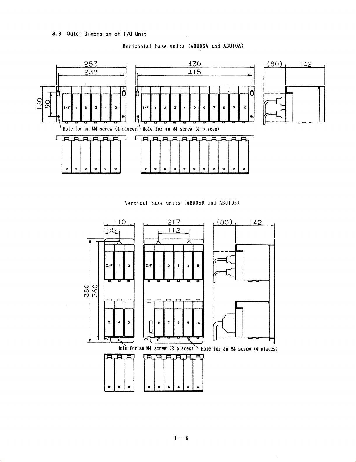
3.3 Outer Bimension of I/O Unit
mm
Horizontal base units (ABUOSA and ABUlOA)
‘Hole for an M4 screw (4
J=L
0
;c
places)’ Hole for an M4 screw (4 places)
I
---
I
I
--
Vertical base units (ABUOSB
I/F
6
Hole fpr an M4 screw (2 places)
and ABUlOB)
\ Hole for an &I4 screw (4 places)
1 -6
Table 3.3 Heat value of each module
I I I I
Module name
I
i
AIFOlA
Xl
.
k2
.
%3
%4
%5
.
.
AIFOlB
p&y+-
.
AID166
.
AID32El
L 0. 1
AID32E2
I_ AID32Fll o-1
AID32F2
_
AIAlGG
Basic heat’
value
I
1
I
1
i:z
-2
. _
0: 1
0. 1
0. I
0.
I ”
pz&& ’
%6
r AOD32Cl
%7
,
AOD32Dl
AOD32D2
AOAO5E
,
AOAO8E 1 -r
AOA12F
1 AOR08G m
AORl 6G
AORl 6H2
AADO4A
I ADAOZA 1 T
1
ACTOlA
0: ;
0.
0. 1
0.
;;: ;
0:
0. 1
3. 1
4. 1 1
1
1
1
1
(W>
2
1
1
1
;
Heat value per
1 I/O point (W>
0.04+
0. 04+
0.04+ 1.4x IL2
0.04+ 1.4x IL2
0. Ol+
0. Ol+
0. Ol+
0.13+
0.13+ 1.5x IL
O.ll+ 1.5x IL
0.3 +
0.3 + 0.1xIL2
0.3 + 0.1xIL2
0. 23
0. 23
0. 21
0. 21
0. 23
0. 23
0. 23
0. 23
0.
21
0.4xIL2
0. 6x IL2
0. 8x IL2
0. 8x IL2
0. 8x IL2
1.5x IL
0.1xIL2
I
.
l TotaI ‘Heat value per 1 I/O point’ for simultaneous ON points plus ‘Basic heat value’
is the heat value of the module.
l 1L:Load current of output
l AOD3201 of
(Example :
‘X1-%7” is the same module as former AID 3 20
A I D 3 2 E 1 is equal to former A I D 3 2 E.)
1
-7
.
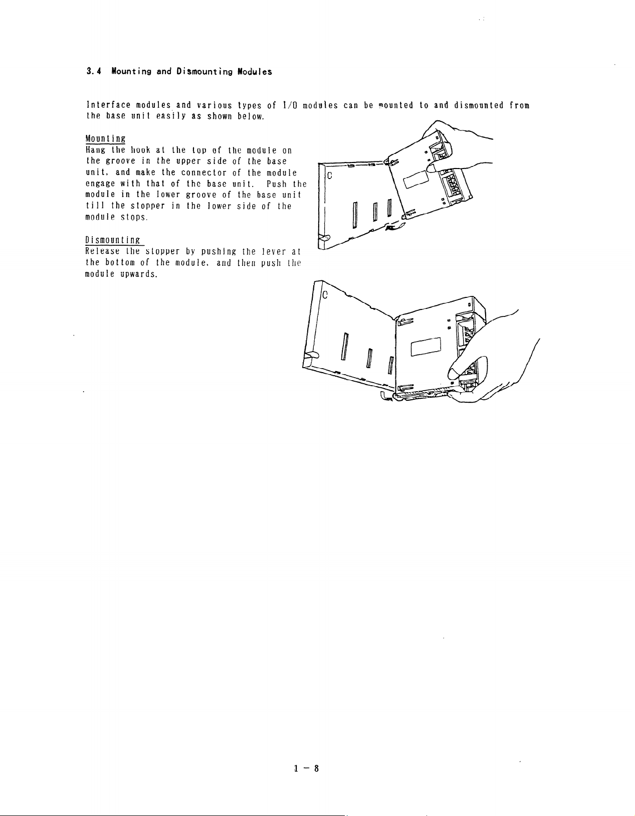
3.4 Mounting and Oismounting ModuJes
Interface modules and various types of I/O modules can be wunted to and dismounted from
the base unit easily i3s shown below.
Mounting
Hang the hook at the top of the module on
the groove in the upper side of the base
_
unit, and make the connector of the module
engage with that of the base unit. Push the
module in the Iower groove of the base unit
till the stopper in the lower side of the
mnriirl P s!ops.
1.. ” Y . a _
Dismounting
Release the stopper by pushing the lever at
the bottom of the module, and then push the
module upwards.
:l - 8
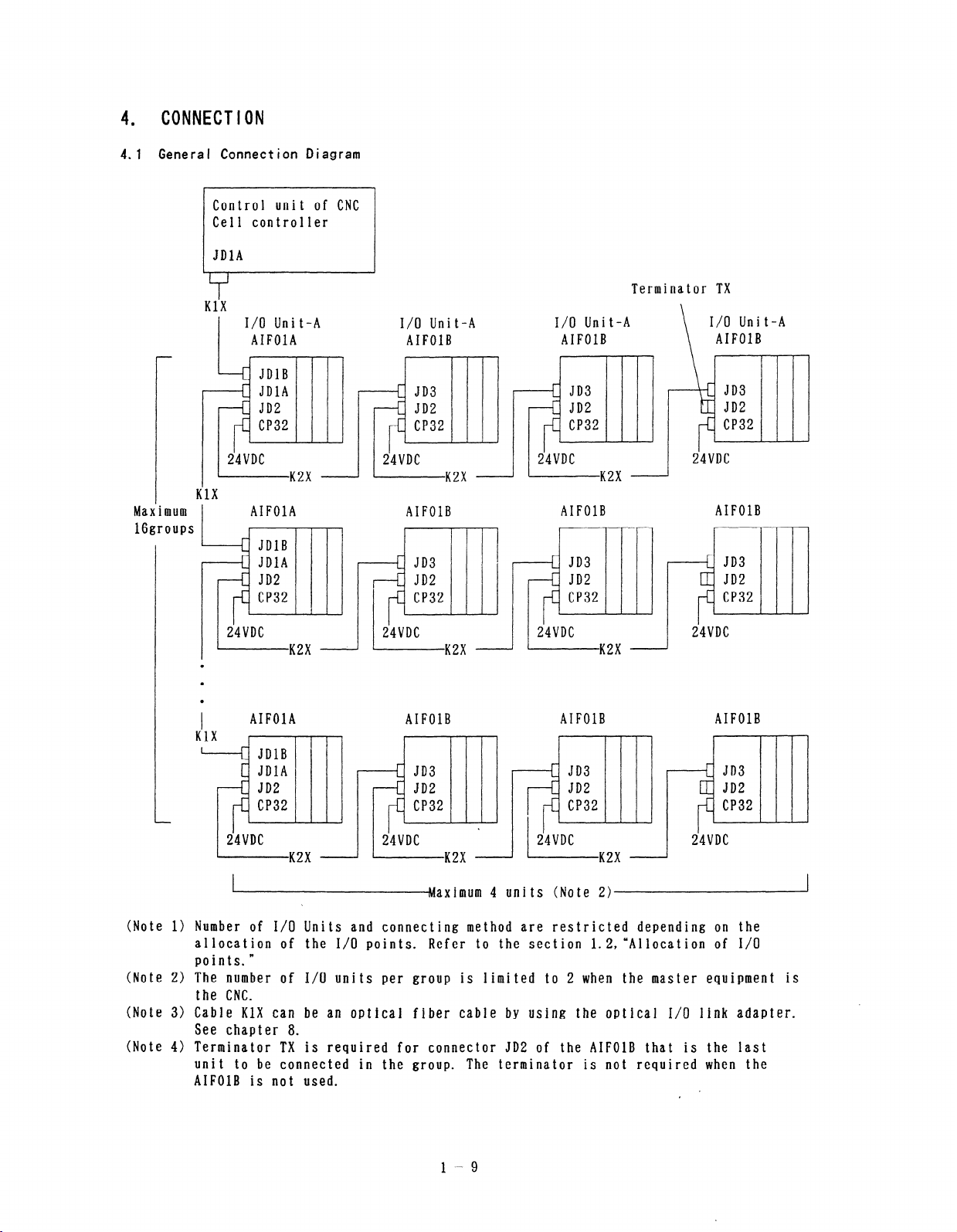
4 . CONNECTION
4.1 General Connect ion Diagram
Control unit of CNC
Cell controller
JDlA
KlX
I
Maximum 1
16groups
0
l
0
I
KlX
I/O Unit-A I/O Unit-A
AIFOIA
r
1 24VDC K2X 1 1 i4VDC K2X 1 1 24VDC K2X
AIFOlA
b
[ JDlB
c JDlA
[ JD2
-c CP32
24VDC
K2X
I
AIFOlA
AIFOlB
t JD3
[ JD2
-c CP32
‘
AIFOlB
AIFOlB
1
I/O Unit-A
AIFOIB
AIFOlB
1 24VDC
;K2X -
AIFOlB AIFOlB
Terminator TX
I/O Unit-A
AIFOlB
i4VDC
__I
AIFOlB
i4VDC
1 i4VDC K2X ] / i4VDC K2X
naximum 4 units (Note 2))
(Note 1) Number of I/O Units and connecting method are restricted depending on the
allocation of the I/O points.
points.”
(Note 2) The number of I/O units per group is limited to 2 when the master equipment is
the CNC.
(Note 3) Cable KlX can be an optical fiber cable by using the optical I/O link adapter.
See chapter 8.
(Note 4) Terminator TX is required for connector JD2 of the AIFOlB that is the last
unit to be connected in the group.
AIFOlB is not used.
Refer to the section l.Z,“Allocation of I/O
The terminator is not required when the
-9
1
.
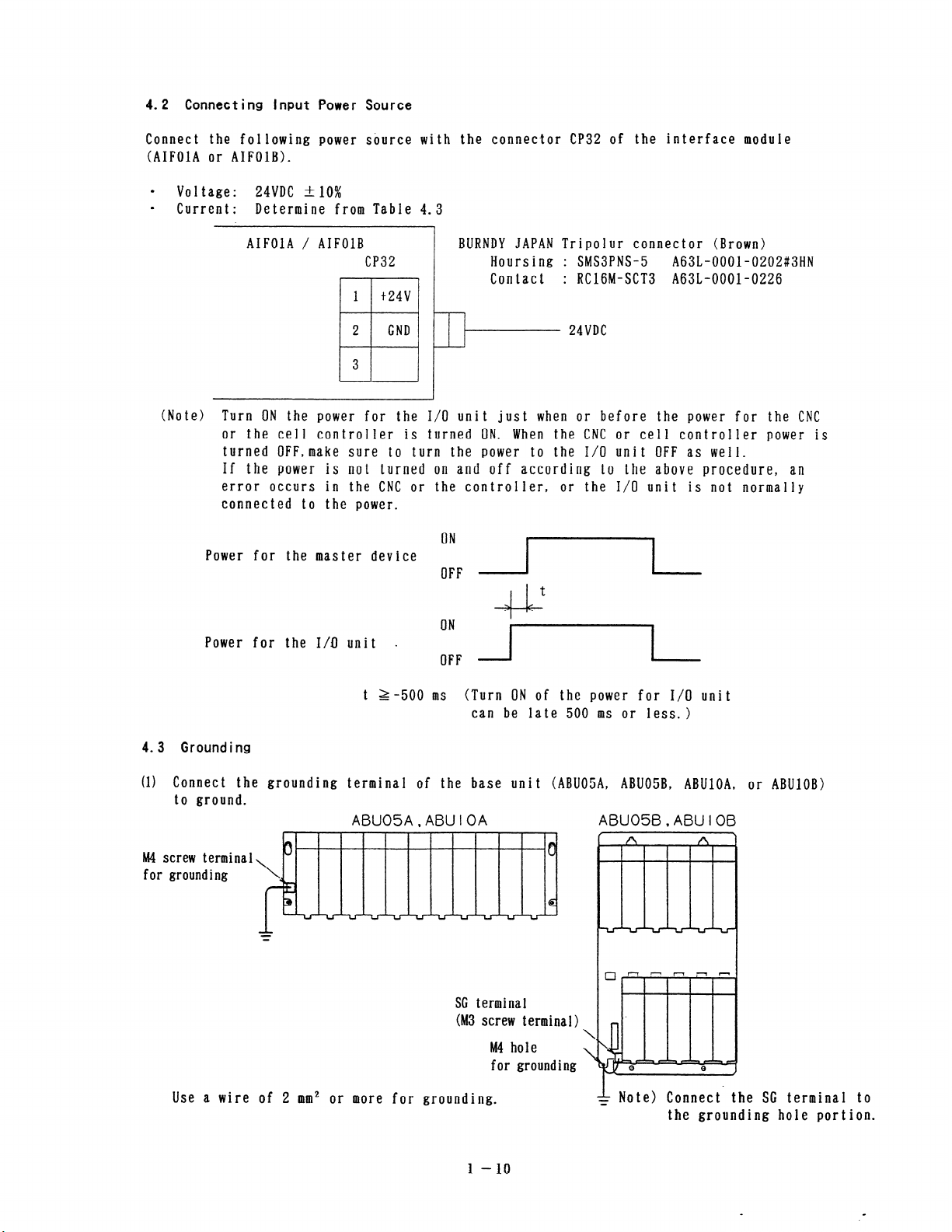
4.2 Connecting Input Power Source
Connect the following power source with the connector CP32 of the interface module
(AIFOlA or AIFOlB).
0
Voltage:
0
Current: Determine from Table 4.3
24VDC t 10%
AIFOlA / AIFOlB
CP32
BURNDY JAPAN Tripolur connector (Brown)
Hoursing
: SMS3PNS-5
A63L-OOOl-0202#3HN
Contact : RClGM-SCT3 A63L-0001-0226
1 t24v
2
GND
24VDC
3
H 1
(Note) Turn ON the power for the I/O unit just when or before the power for the CNC
or the cell controller is turned ON. When the CNC or cell controller power is
turned OFF,make sure to turn the power to the I/O unit OFF as well.
If the power is not turned on and off according to the above procedure, an
error occurs in the CNC or the controller, or the I/O unit is not normally
connected to the power.
Power for the master device
::F r
t
++J+
Power for the I/O unit -
::F E
t Z-500 ms (Turn ON of the power for I/O unit
can be late 500 ms or less. >
4.3 Grounding
(1) Connect the grounding terminal of the base unit (ABU05A, ABU05B, ABUlOA,
to ground.
ABUOSA,ABUlOA
ABUO58,ABUiOB
M4 screw terminal
for grounding
SC terminal
(M3 screw terminal)
M4 hole
\
\
for grounding
Use a wire of 2 mm2 or more for grounding.
+ Note) Connect the SC terminal to
the grounding hole portion.
or ABUlOB)
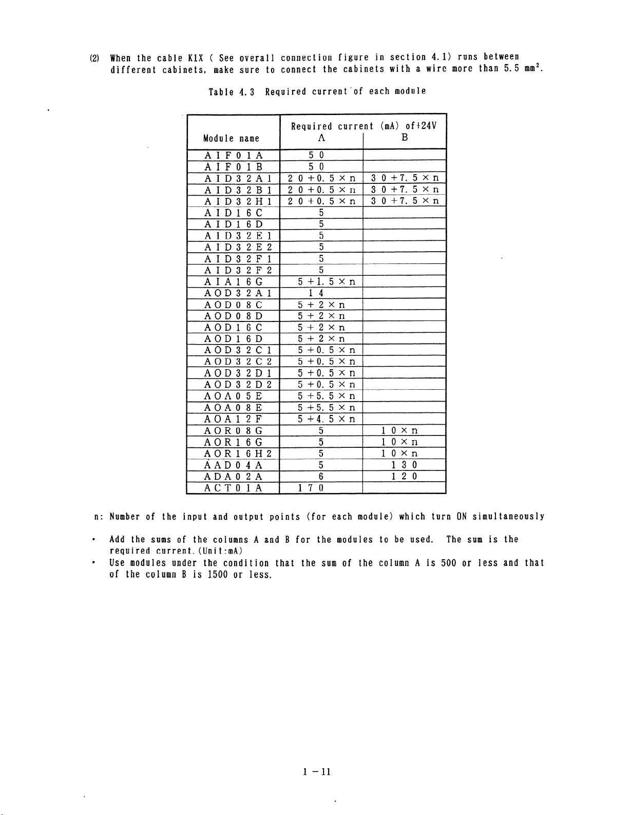
(2) When the cable KlX ( See overall connection figure in section 4.1) runs between
different cabinets, make sure to connect the cabinets with a wire more than 5.5 mm2.
Table 4.3 Required current’of each module
Required current (mA) of+24V
Module name
AIFOlA
AIFOlB
AID32Al
AID32Bl
AID32Hl
AID16C
AID16D
AID32El
AID32E2
AID32Fl
AID32F2
AIAlGG
AOD32Al
AODO8C
AODO8D
AOD16C
AODl 6D
AOD32Cl
AOD32C2
AOD32Dl
AOD32D2
AOAO5E
AOAO8E
AOAlZF
AORO8G
AORl 6G
AORl 6H2
AADO4A
ADAOZA
ACTOIA
A
5 0
5 0
20+0.5xn
20+0.5xn
20+0.5xn
5
5
5
5
5
5
5+1.5xn
14
5+2Xn
5+2xn
5+2xn
5+2Xn
5+0.5Xn
5+0.5xn
5+0.5xn
5+0.5xn
5+5.5xn
5+5.5xn
5+4.5xn
5
5
5
5
6
170
B
.
30+7.5xn
30+7.5xn
30+7.5xn
1OXn
1Oxn
1Oxn
13 0
12 0
n: Number of the input and output points (for each module) which turn ON simultaneously
0
Add the sums of the columns A and B for the modules to be used. The sum is the
required current. (Unit:mA)
0
Use modules under the condition that the sum of the column A is 500 or less and that
of the column B is 1500 or less.
l-11
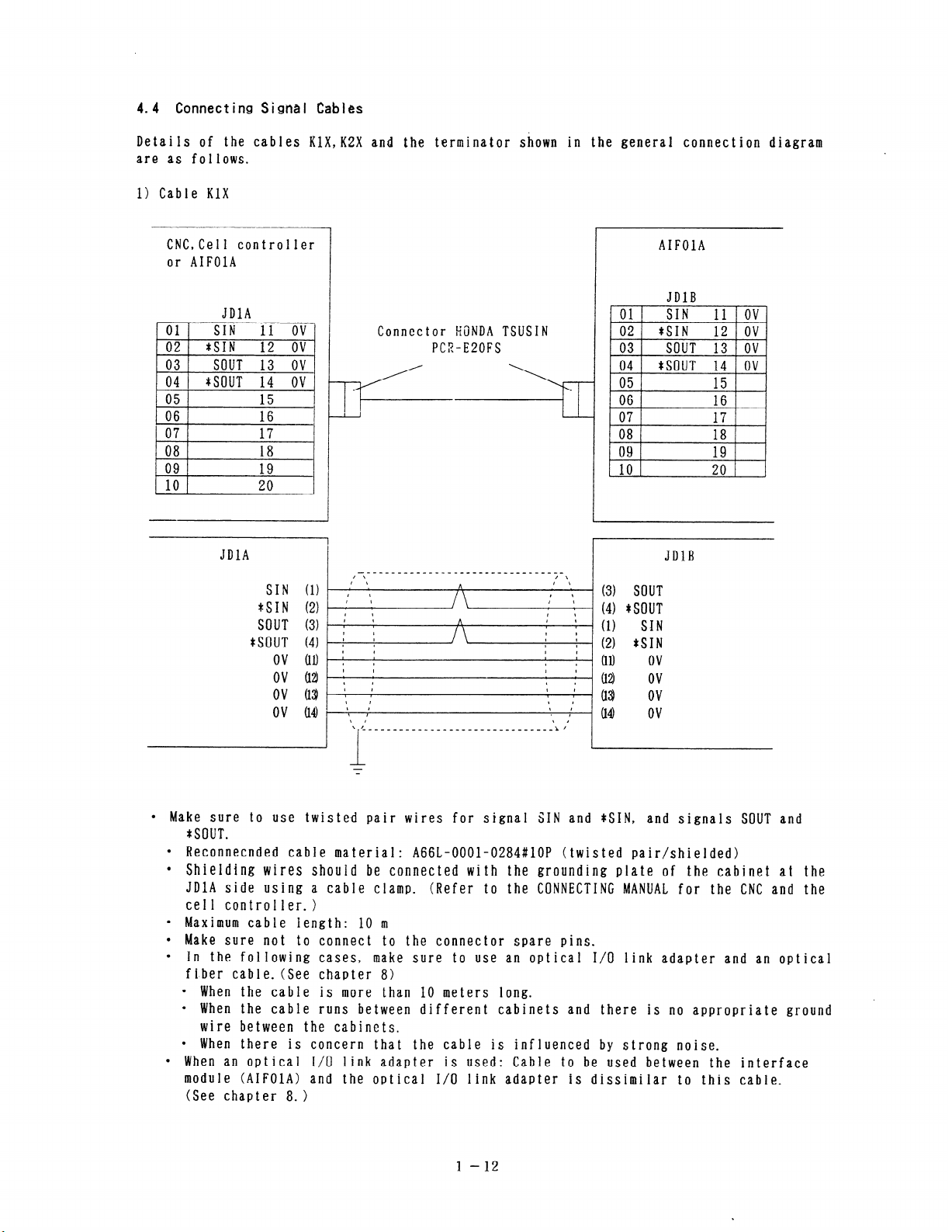
4.4 Connecting Signal Cables
Details of the cables KlX,KZX and the terminator shown in the general connection diagram
are as follows.
1) Cable KlX
CNC, Cell controller
or AIFOlA
JDlA
’ 01 SIN 11 ov
02 GIN
03 SOUT
.
GOUT 14 OV
04
,
05
06
07
08
.
09
10
12 ov
13 OV
15
16
17
18
19 .
20
JDlA
SIN (1) 1’ ‘\a,
*SIN (2) (’ :
SOUT (3) L i :
*SOUT (4) i i
ov (11). i i
ov (18, : I
ov (13 r :
ov (l4) ‘\I /
Connector WNDA TSUSIN
PC%-EZOFS
1
I
____________________~~~~~~~~~~~~~
h
A
:
\ I
‘,C__ 1 ____________________~~~~~~~~
/ \
I \
f 1
, 1
8
I I
1
1 I
I
, I
t
, ,
\ I
8 I
\ I
L/
t
(3) SOUT
(4) *SOUT
(1)
I
(2) *SIN
I
(11)
I
(12)
I
,
03)
(14)
AIFOlA
JDlB
\I
JDlB
SIN
ov
ov
ov
ov
-
l Make sure to use twiste.d pair wires for signal SIN and *SIN, and signals SOUT and
*SOUT.
l Reconnecnded cable material: A66L-OOOl-0284#10P (twisted pair/shielded)
l Shielding wires should be connected with the grounding plate of the cabinet at the
JDlA side using a cable clamp.
(Refer to the CONNECTING MANUAL for the CNC and the
ccl 1 controller. >
l Maximum cable length: 10 m
l Make sure not to connect to the connector spare pins.
l In the following cases, make sure to use an optical T/O link adapter and an optical
fiber cable. (See chapter 8)
l When the cable is more than 10 meters long.
l When the cable runs between different cabinets and there is no appropriate ground
wire between the cabinets.
l When there is concern that the cable is influenced by strong noise.
l When an optical I/O link adapter is used: Cable to be used between the interface
module (AIFOlA) and the optical I/O link adapter is dissimilar to this cable.
(See chapter 8. >
l-12
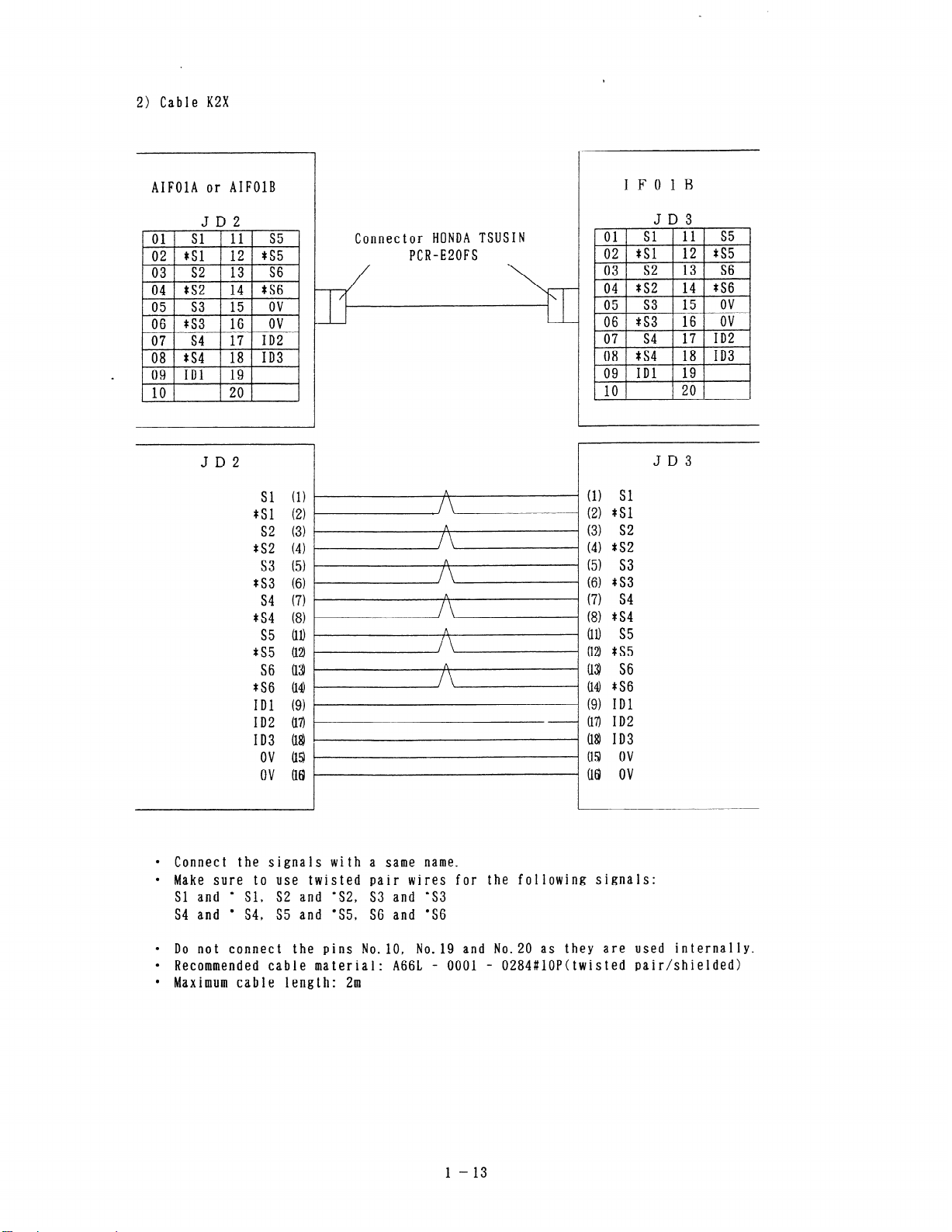
2) Cable KZX
AIFOlA or AIFOlB
ti
08 *S4 18 ID3
.
09 ID1 19
JD2
JD2
Sl (1)
*Sl (2)
s2 (3)
*s2 (4)
s3 (5)
*S3 (6)
s4 (7)
*S4 (8)
s5 (11)
*s5 (12)
S6 U3)
*S6 (14)
ID1 (9)
ID2 U?)
ID3 U8)
ov (153
ov 08
IFOlB
JD3
Connector HONDA TSUSIN
PCR-EZOFS
JD3
(1) Sl
(2) *Sl
(3) s2
(4) *s2
(5) s3
(6) *s3
(7) s4
(8) *S4
(11) s5
(12) *s5
(13) S6
(14) *S6
(9) ID1
(I?) ID2
(18) ID3
u53 ov
(18 ov
l Connect the signals with a same name.
l Make sure to use twisted pair wires for the following signals:
Sl and *
S4 and *
l Do not connect the pins No.10, No.19 and No.20 as they are used internally.
l Recommended cable material: A66L - 0001 -
l Maximum cable length: 2m
Sl, S2 and +S2, S3 and ‘S3
S4, S5 and *S5, S6 and ‘S6
0284#10P(twisted pair/shielded)
1 - 13
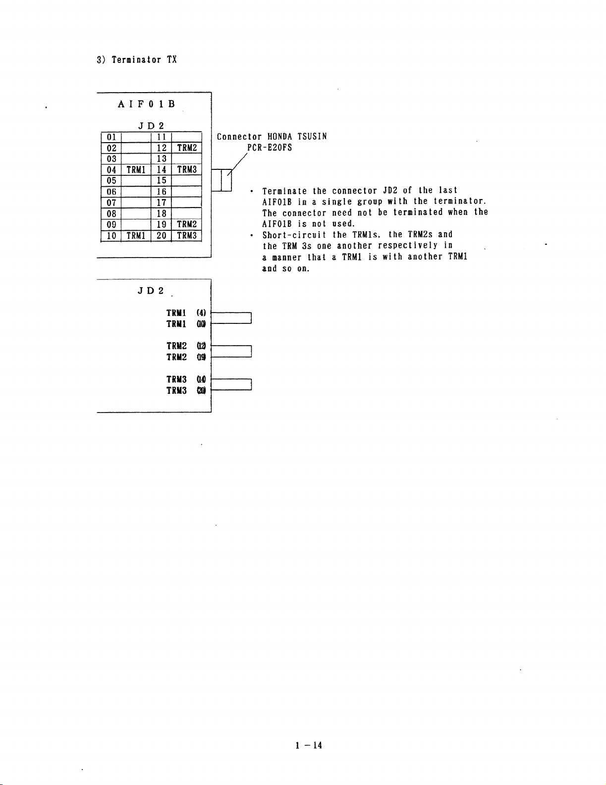
3) Terminator TX
AIFO1B
JD2
I
Connector HONDA TSUSIN
PCR-EZOFS
l Terminate the connector JD2 of the Iast
AIFOlB in a single group with the terminator.
The connector need not be terminated when the
AIFOlB is not used.
l Short-circuit the TRMls, the TRMZs and
the TRM 3s one another respectively in
a manner that a TRW is with another TRW
and so on.
’
I-14
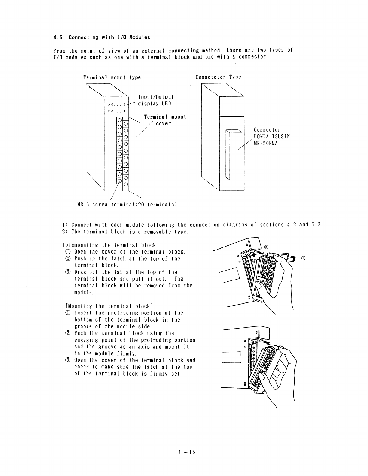
4.5 Connecting with J/O Modules
From the point of view of an external connecting method, there are two types of
I/O modules such as one with a terminal block and one with a connector.
Terminal mount type
Connetctor Type
Input/Output
A~. . . 7,‘display LED
Terminal mount
cover
/
Connect or
HONDA TSUSIN
/” MR-50RMA
\
M3.5 screw terminal(20 terminals)
1) Connect with each module following the connection diagrams of sections 4.2 and 5.3.
2) The terminal block is a removable type.
[Dismounting the terminal block]
0 Open the cover of the terminal block.
@ Push up the latch at the top of the
terminal block.
@ Drag out the tab at the top of the
terminal block and pull it out.
The
terminal block will be removed from the
module.
[Mounting the terminal block]
@ Insert the protruding portion at the
bottom of the terminal block in the
groove of the module side.
@ Push the terminal block using the
engaging point of the protruding portion
and the groove as an axis and mount it
in the module firmly.
@ Open the cover of the terminal block and
check to make sure the Iatch at the top
of the terminal block is firmly set.
l-15
3) Cautionary paints when wiring terminal block type
l Wiring material : AWGZZ - 18 (0.3-O. 75 mrn2)
A wire as this as possible. is recommended.
l Crimp style terminal : (43.5
Crimp style terminal with no insulation sleeve and a short
distance “A”,
as illustrated in the drawing below, is
recommended.
A
Pi
0
m
l Mark tube: Use a short mark tube as possible and cover crimped part with the mark
DAIDO TANSHI
NICHIFU TANSHI
1.25-s3.5
1.25-3. 5s etc.
tube.
‘1 -16
5
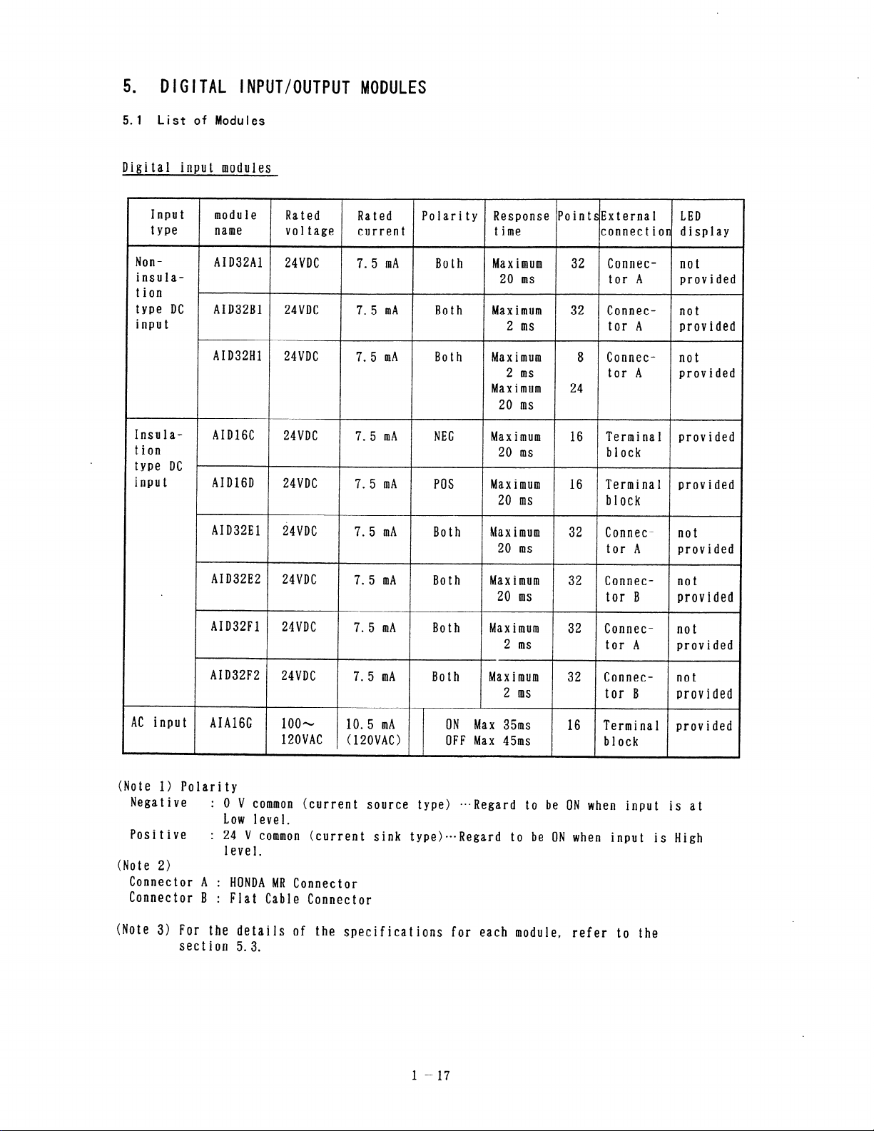
. DIGITAL INPUT/OUTPUT MODULES
5.1 List of Modules
Digital input modules
Input module
type
Non-
AID32Al
insulation
type DC
input
Insula-
AID32Bl
AID32Hl
AIDIGC
tion
type DC r
input
AIDlGD
AID32El
AID32E2
AID32Fl
name
Rated Rated Polarity Response PointsExternal
voltage current
24VDC
7. 5 mA
Both
time
Max imum 32 Connec- not
connection display
20 ms tor A provided
24VDC
24VDC
7. 5 mA
7.5 mA
Both Max imum 32 Connec- not
2 ms
Both Maximum 8
2 ms
tor A provided
Connec-
tor A provided
Maximum 24
20 ms
24VDC 7.5 mA NEG
24VDC
7.5 mA POS
Maximum 16 Terminal provided
20 ms
block
Maximum 16 Terminal provided
20 ms block
24VDC
24VDC
7.5 mA Both
7.5 mA
Both Maximum 32
Max imum 32
20 ms
Connec- not
tor A provided
Connec- not
20 ms tor B
24VDC
7.5 mA Both Maximum 32 Connec2 ms tor A provided
LED
not
provided
not
AI D32F2
24VDC
7.5 mA Both Maximum 32
Connec- not
2 ms tor B
AC input
AIAlGC loo--
120VAC
10.5 mA ON Max 35ms 16
( 120VAC > OFF Max 45ms
Terminal provided
block
(Note I> Polarity
Negative :
0 V common (current source type)
l ==Regard to be ON when input is at
Low level.
Positive
: 24 V common (current sink type)*==Regard to be ON when input is High
level.
(Note 2)
Connector A :
Connector B :
HONDA MR Connector
Flat Cable Connector
(Note 3) For the details of the specifications for each module, refer to the
section 5.3.
l-17
provided
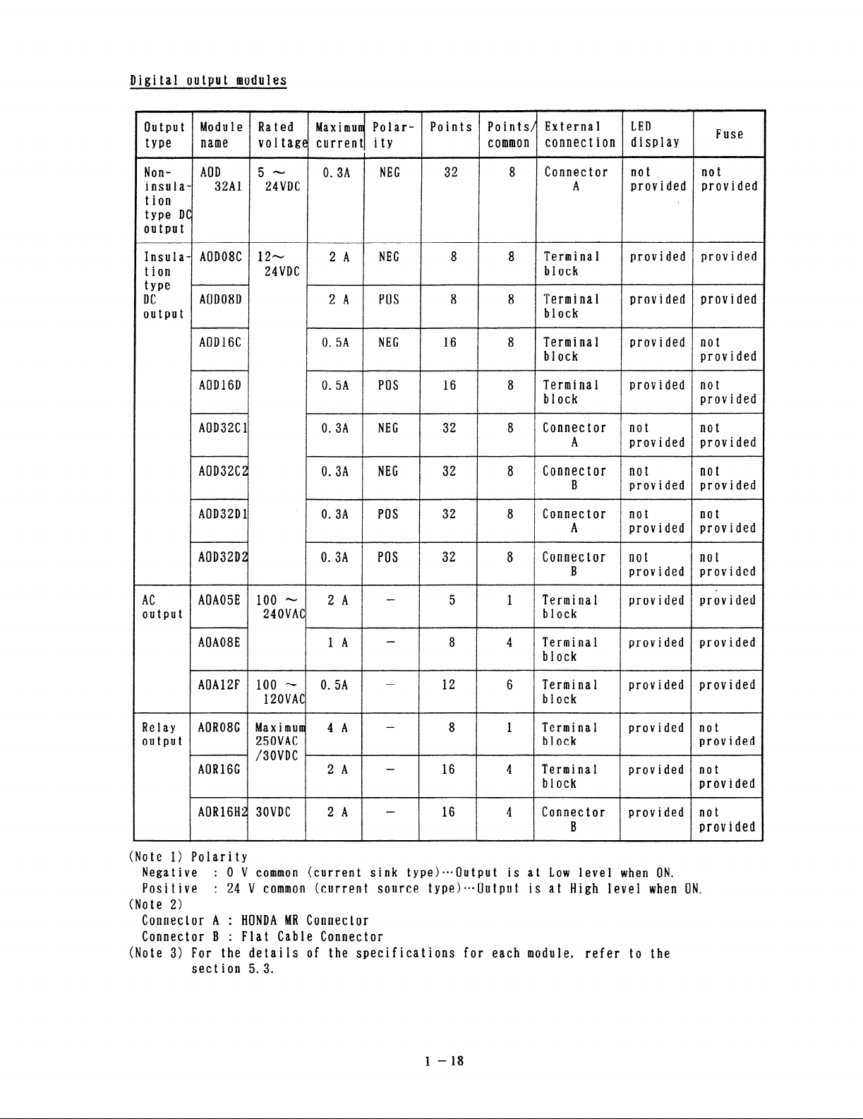
Digital output modules
Output Module Rated Maximum Polar-
type
name
Non- AOD 5 - 0. 3A
voltage current ity
NEG 32 8 Connector not
insula- 32Al 24VDC
tion
type DC
output
Insula- AOD08C 12- 2 A
tion
fYPe f
DC
AOD08D 2 A POS 8 8
24VDC
NEC 8 8 Terminal provided
output
AODl6C 0. 5A NEC 16 8
AOD16D 0. 5A POS 16 8
AOD32C 1 0. 3A NEG 32 8
AOD32C2 0. 3A
NEG 32 8 Connect or not
AOD32D 1 . 0. 3A POS 32 8
Points Points/ External
common
connection display
A provided provided
block
Terminal provided provided
block
Terminal provided not
block
Terminal provided not
block
Connect or not not
A provided provided
B provided provided
Connector not not
A
LED
Fuse
not
provided
provided
provided
not
provided provided
AOD32D2 0. 3A POS 32 8
Connect or not not
B provided provided
AC
AOA05E 100 - 2 A - 5 1
output 240VAC
AOA08E 1A - 8 4
Terminal provided provided
block
Terminal provided provided
block
Terminal provided provided
block
Terminal provided not
block provided
Relay
output
AOAlZF 100 - 0.5A - 12 6
120VAC
AOR08G Maximum 4 A - 8 1
250VAC
l /30VDC
AORl6G 2A
- 16 4 Terminal provided
block provided
AOR16H2 30VDC 2 A - 16 4
Connector provided not
B provided
(Note 1) Polarity
Negative
Positive
: 0 V common (current sink type)-•=Output is at Low level when ON.
: 24 V common (current source type)===Output is at High level when ON.
(Note 2)
Connector A :
Connector B
HONDA MR Connector
: Flat Cable Connector
(Note 3) For the details of the specifications for each module, refer to the
sect ion 5.3.
not
1
l-18
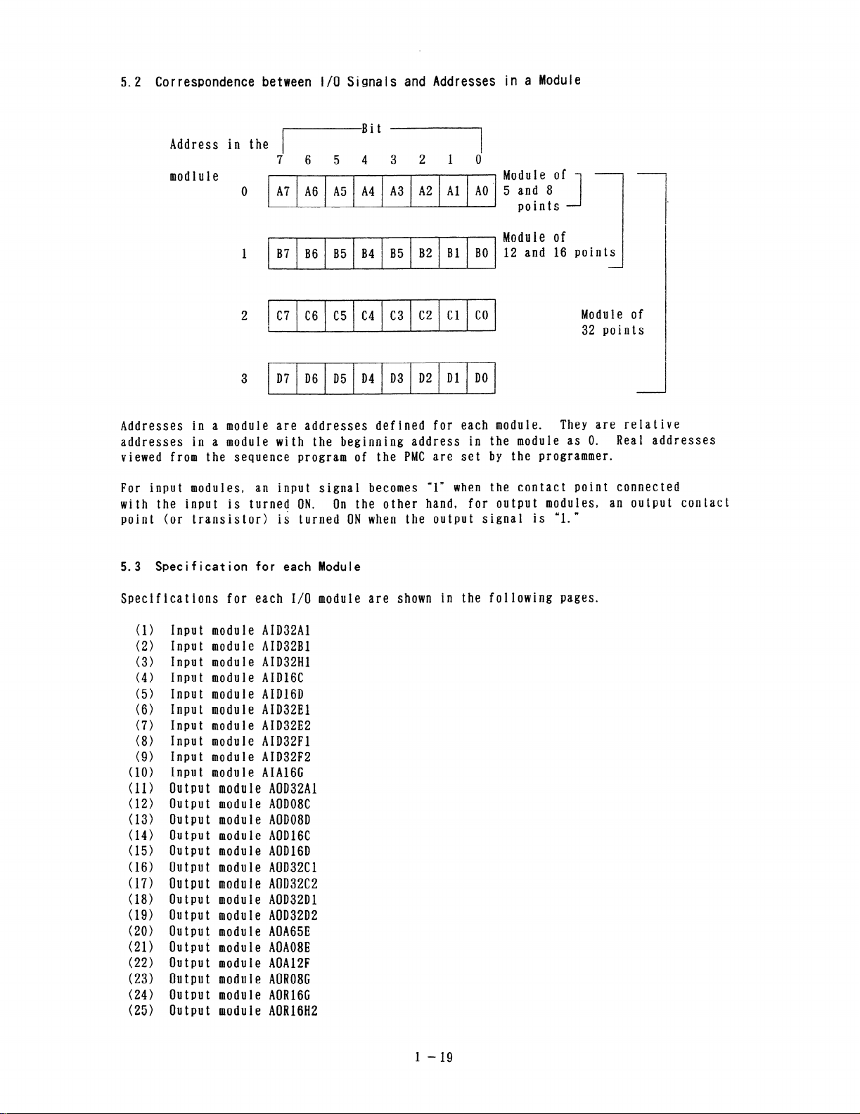
5.2 Correspondence between l/O Signals and Addresses in a Module
Address in the
modlule
‘7 6 5
A7 A6 A5 A4 A3 A2 Al AO’ 5 and 8
0
4 3 2 1 0
4 Module of
) points
. Module
B7 B6 B5 B4 B5 B2 Bl BO 12 and 16 points
1
2
C? C6 C5 C4 C3 C2 Cl CO
D7 D6 D5 D4 D3 D2 Dl DO
3
Addresses in a module are addresses defined for each module.
addresses in a module with the beginning address in the module as 0.
viewed from the sequence program of the PMC are set by the programmer.
For input modules,
with the input is turned ON.
point (or transistor) is turned ON when the output signal is ‘l/
5.3 Specification for each Module
Specifications for each I/O module are shown in the following pages.
(1) Input module AID32Al
(2) Input module AID32Bl
(3) Input module AID32Hl
(4) Input module AID16C
(5) Input module AIDl6D
(6) Input module AID32El
(7) Input module AID32E2
(8) Input module AID32Fl
(9) Input module AID32F2
(10) Input module AIAlGC
(11) Output module AOD32Al
(12) Output module AOD08C
(13) Output module AOD08D
(14) Output module AOD16C
(15) Output module AOD16D
(16) Output module AOD32Cl
(17) Output module AOD32C2
(18) Output module AOD32Dl
(19) Output module AOD32D2
(20) Output module AOA65E
(21) Output module AOA08E
(22) Output module AOA12F
(23) Output module AOR08C
(24) Output module AOR16C
(25) Output module AORl6H2
an input signal becomes
On the other hand, for output modules, an output contact
“1” when the contact point connected
of
Module of
32 points
They are relative
Real addresses
l-19
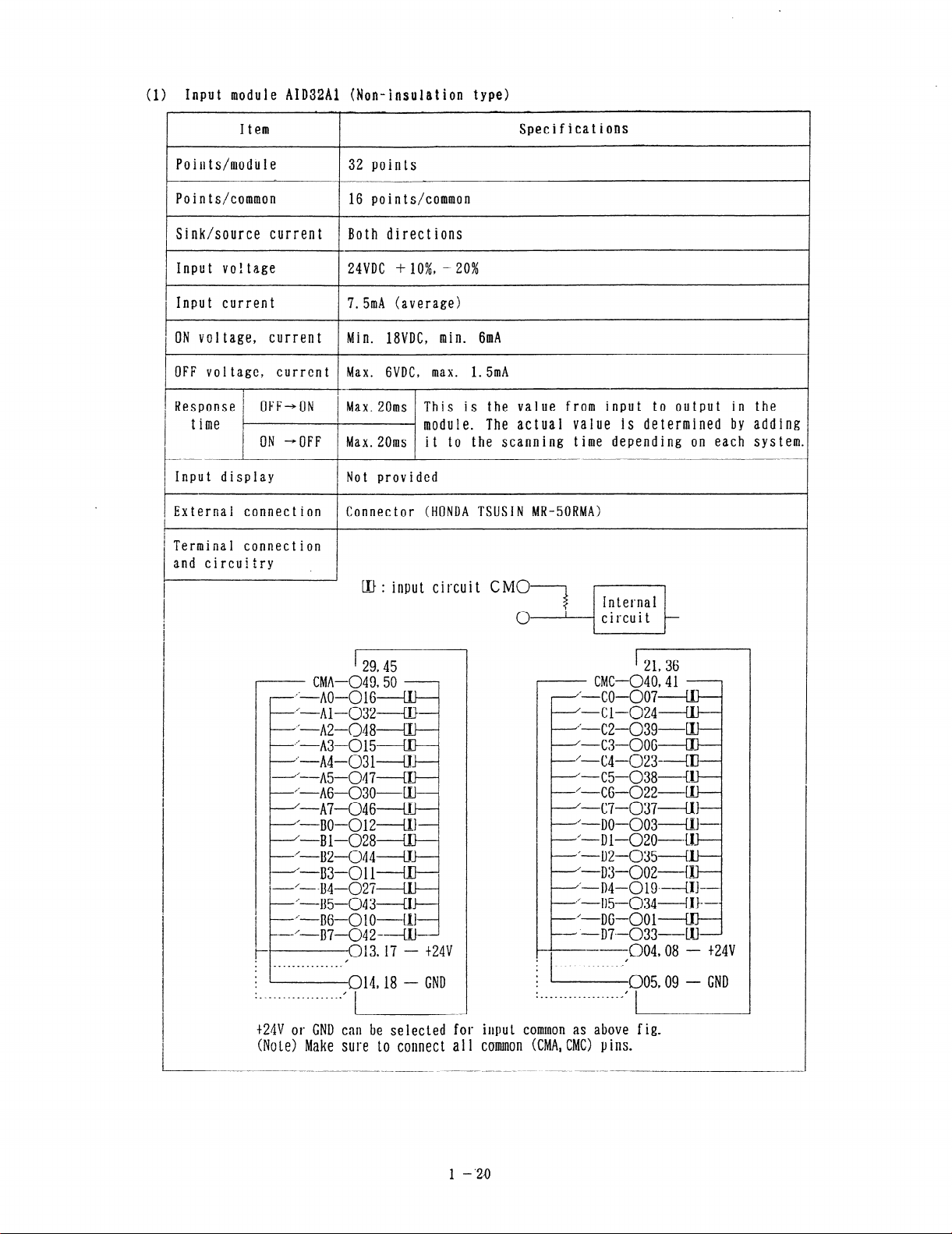
> Input module AID32Al (Non-insulation type)
(1
Item
9
Specifications
Points/module
Points/common
/ Sink/source current
Input voltage
I
1 Input current 7.5mA (average)
I
1 ON voltage, current Min. 18VDC, min. 6mA
32 points
pp/Ipoints/cammon ~~ ~~
Both directions
24VDC + IO%, - 20%
1 OFF voi ‘4”‘0,:“‘::“’ 1 Max. GVDC, max. 1.5mA
/ Response 1
time
Input display
External connection
*
1
Oh - OFF Max.20ms it to the scanning time depending on each system
Max.20ms This is the value from input to output in the
’ module. The actual value is determined by adding
Not provided
Connector (HONDA TWIN MR-50RMA)
Terminal connection
and circuitry
I
I
’ LU : input circuit CMO--7 I------J
r I
’ 29,45
CMA-049.50
--~*-_A@---_Ol~ LI)
I .‘--Al-0324 -
#=-----AZ-048 W 3
’ *‘----A3-015 Kt a
:‘----A4-_031----c!~
---A5--047--+1~
’ “---A6-03o-w
. ‘-A7-046-----LU 1
‘-BO-012---+1
-Bl-028 Ul
,‘-BZ-044----#
1 ~;B3-011+~ 1
‘--B4-027-----t
‘~~5~~43~~~
4
n&--0 10-41
---‘-U7----042------W-
t-
. /
; l“‘___“__“‘_.. 014 18 _ GND
.
._---..---..___._-.
013,17 - t24v
‘L
t24V or GNU can be selected for
(N0t.e) Make sure to connect all
’ 21,36
- CMC-040,41 - 1
- I---CO-007--+ ti -
‘-Cl-024----I 1 _
“-c2-_039--4 I---
‘-C3--_00G-----l Ll a
h ‘---X4-023---! 3 -
‘-C5-038-------i J
‘-c&-022--+ I)- ’
‘-c7---037---l I1 ’
‘-DO-003-i I)---
’ ~‘---+--020--i J 4
- l ‘---D2-035---i I)
‘-D3-002--t 13 -
* L-j)4-019--_-I ‘f---
* ‘-D5-034-----l ‘I---
p -‘-DE-001---4 r) 1
--.-----D7--_033----[ IJ -
; i___....:?); 1; 1 ;;;
.
. ,
.___-_._---_.--._-C
I
I
input common as above fig.
cormnon (CMA, CMC) y ins.
9
1 -‘20
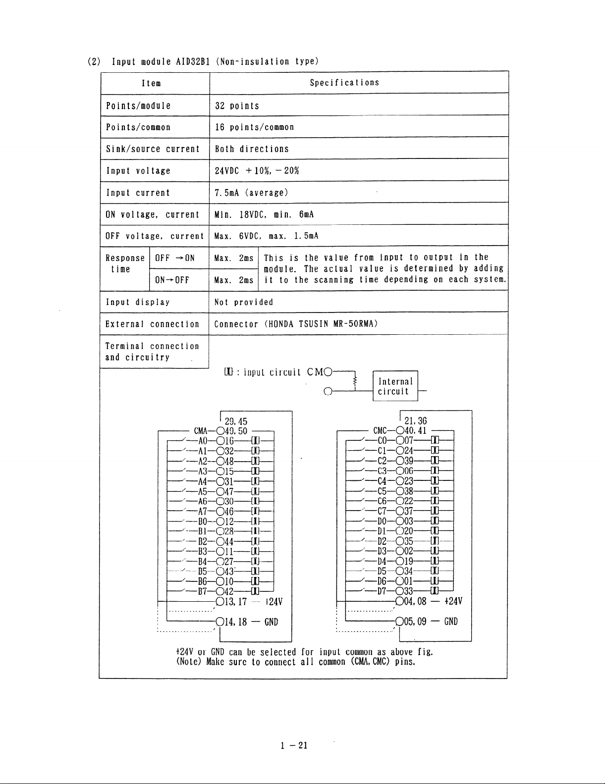
(2) Input module AID32Bl (Non-insulation type)
Item
Points/module
32 points
Specifications
Points/common 16 points/common
Sink/source current Both directions
Input voltage 24VDC + lo%, - 20%
Input current 7.5mA (average)
ON voltage, current Min. IWDC, min. 6mA
OFF voltage, current Max. GVDC, max. 1. 5mA
Response OFF -+ON
time
ON-OFF Max. 2ms
Max. 2ms This is the value from input to output in the
module. The actual value is determined by adding
it to the scanning time depending on each system.
Input display Not provided
External connection Connector (HONDA TSUSIN MR-SORMA)
LT-F: input circuit CM0
1
[ 29.45
- CMA-049950
c ~‘-no-Olk---4IJ .
c ‘--Al-032~El 1
~~-----1\2--048~~~~
*‘---A3-015-----EIJ
J--A4-03 l-l!u _
‘-n5-047---u.l
---a”-AG-030------W
SO’-A7-046~[I$----.
-~--Bo--012--ut-
--~‘--B1-028+!1-
. “-B2--044------U .
- I---+3-01 1------ul-----
n,F--B4-027----q]---
* -‘--.B5-043~LIl *
‘-B6-010 III----
L ‘-BP-042-----W $
013,17 - t24v
-t
i --014.18 - CND
.---.-a.__ . . . .._...
,
- CMC-040941
. ‘-co-007 III A
---‘-Cl-024~El .
* ‘-c2-_039---a-----
‘-c3-006 m ’
. ‘--C4-023 El
. ‘-C5-038
=-CS-022 El I
-“-c7--037 al ’
-‘-DO-003 rn
j’-Dl-020 III
‘-D2-_035-----El
1 l’-D3-002-----W 1
-‘-Dull-019---rrl 1
.‘---D5-034----W
’ /--DC-001-Lu ’
- d’-D7-033
___w_-..m.___-..
.
.
*
. +
.
‘ ,
..______.____*.___..
‘I
t24V or CND can be selected for input common as above fig.
(Note> Make sure to connect a 1 I common WAIA, CM0 pins.
J
L 21936
004,08 - t24V
/
005,09 - CND
I
1-21 .
(3) Input rsodule AID32Hl
Item
I
Specifications
Points/module
Points/common
Sink/source current
Input voltage
Input current
ON voltage, current
OFF voltage, current
Response OFF *ON
time
ON-OFF Max. 2ms (AOmA7) ing time depending on each system.
Input display
External connection
Terminal connection
and circuitry
32 points
16 points/common
Both direct ions
24VDC + lo%, - 20%
7.5mA (average)
Min. 18VDC, min. 6mA
Max. GVDC, max. 1. 5mA
Max. 2ms (AO-A7) This is the vaiue from input tp output
Max. ZOms(BO~D7) in the module. The actual -value is
determined by adding it to the scann-
Max. 20ms (BOhD7)
Not provided
Connector (HONDA TSUSIN MR-50RMA)
cft: input circuit CM 01
I------I
-------013,17 - t24v
. ~~~~.~..~~.~~~~
*
I
.
.
I
. .- _ Wm. _. - I.__. _ __.
I
Q14,18 - CND
,
I
i '-----a5,09 - GND
. /
.--.--------..--a-.*
t24V or C;ND can be selected for input common as above fig.
(No tc> Make sure to comet t a 11 common KMA, CMC) p ins.
1 -22
I
(4) Input module AIDlGC
Item
Points/module
points/common
16 points
16 points/common
Specifications
Sink/source current Source current type
Input voltage
Input current
ON voi tage, current
24VDC + lo%, - 20%
7. 5mAcaverage)
Min. ISVDC, min. 4mA
OFF voltage, current Max. SVDC, max. 1.5mA
Response OFF *ON
Max.ZOms This is the value from input to output in ‘the
time - module. The actual value is determined by adding
ON *OFF
Input display
Extermal connection
Max.ZOms it to the scanning time depending on each system.
LED display
Terminal block connector@0 terminals,M3.5 screw terminal)
Terminal connection
and circuitry .
I
[I): input circuit
1 -23
LED{{
(5) Input module AID16D
Specifications
I
I
OFF voltage, current
I
Input display
I
16 points
16 Dointdcommon
__ r--- -_L,
Sink current type
UVDC +IO%, -20%
Min. 15VDC, min. 4mA
Max. SVDC, max. 1. 5mA
LED display
- _ ___ ___ _ - _
This is the value from input to output in the
module. The actual value is determined by adding
it to the scanning time depending on each system.
I
-_- -
__-f- _@
__c_ b-i.
‘-
‘- -@-t
-----
_-‘-
- - ---
- e
--
--o--ru--_l
@
5 I
rm
-
-‘-’
111 P _.
-_
+’ - FE;/
-e
_I__--
-. --fl543-------c1
-Ml
,’
L-E’
_-__~~-~___
--I
WI
-u_w--1~~-
@
49
@
l- --w- -_ _.
TPl
4J-J
LU : input circuit
1 -,24
LED ff
Loading...