


DM74ALS652WMX
© 2000 Fairchild Semiconductor Corporation DS009174 www.fairchildsemi.com
October 1986
Revised March 2000
DM74ALS652 Octal 3-STATE Bus Transceiver and Register
DM74ALS652
Octal 3-STATE Bus Transceiver and Register
General Description
This device incorpora tes an octal t ransceiver a nd an octal
D-type register configured to enable transmission of data
from bus to bus or internal register to bus.
This bus transceiver features totem-p ole 3-STATE outputs
designed specifically fo r driving highly-capacitive or rela-
tively low-impedance loa ds. Th e hi gh -im ped ance state and
increased high level logic drive provide this device with the
capability of being connected directly to and driving the bus
lines in a bus organized system with out need for interfa ce
or pull-up components. They are par ticularly attractive for
implementing buffer registers, I/O ports, bidirectional bus
drivers, and working registers.
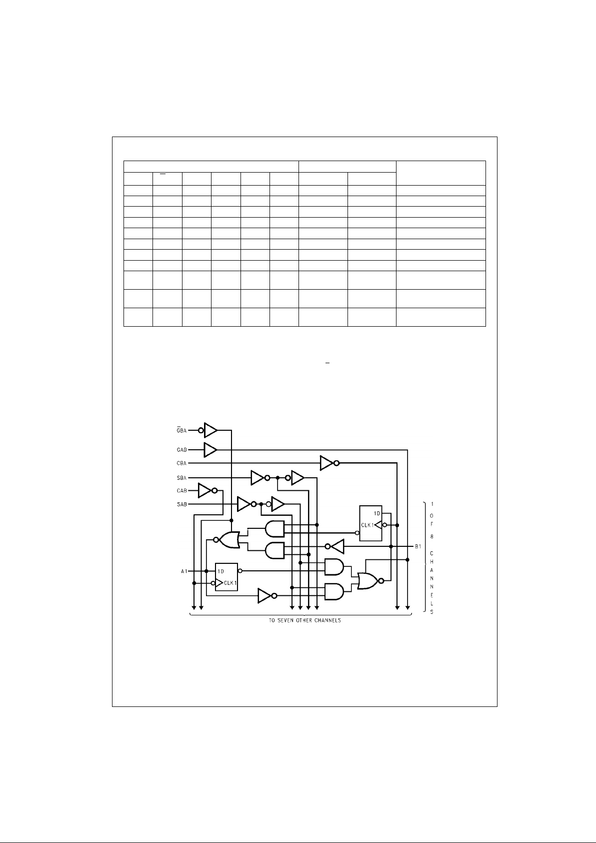
The registers in the DM74 ALS652 are edge-triggered D-
type flip-flops. On the positive tra nsition of the clock ( CAB
or CBA), the input data is stored into the appropr i ate reg is-
ter. The CAB input controls the trans fer of data into the A
register and the CBA input controls the B register.
The SAB and SBA control pins are provided to select
whether real-time data or stored data is transferred. A LOW
input level selects real-time data and a HIGH level selects
stored data. The select controls have a “make before
break” configuration to eliminate a glitch which wo uld nor-
mally occur in a typical multiplexer during the transition
between stored and real-time data.
The enable (GAB and G
BA) control pins provide four
modes of operation: r eal-time data transfe r from bus A to
B, real-time data t ransfer from bus B to A, real-ti me bus A
and/or B data transfer to internal storage, or internal stored
data transfer to bus A and/or B.
Features
■ Switching specifications at 50 pF
■ Switching specifications guaranteed over full tempera-
ture and V
CC
range
■ Advanced oxide-isolated, ion-implanted Schottky TTL
process
■ 3-STATE buffer-type outputs drive bus lines directly
■ Independent registers and enables for A and B buses
■ Multiplexed real-time and stored data
Ordering Code:
Devices also availab le in Tape and Reel. Specify by appending th e s uffix let t er “X” to the ordering code.
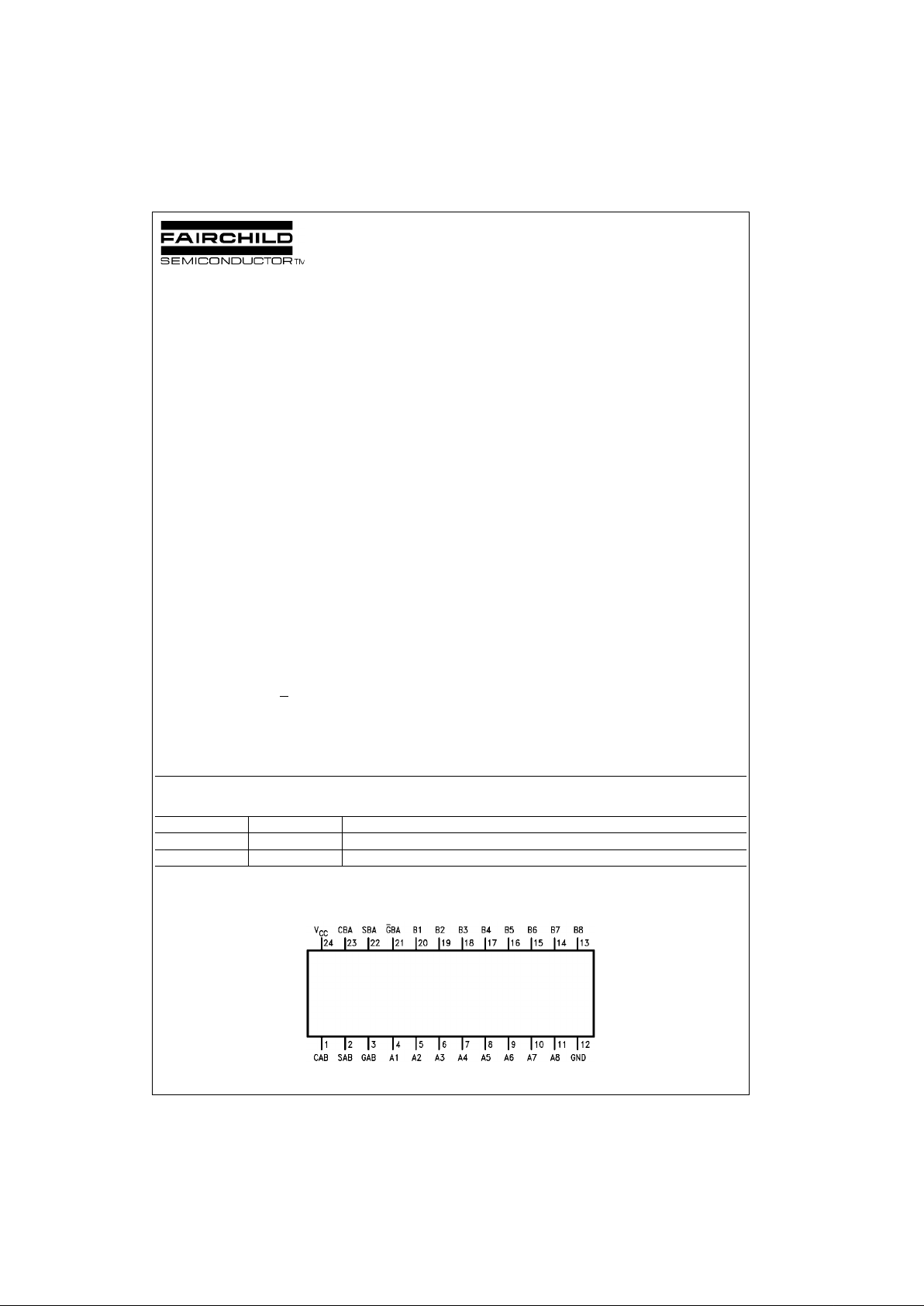
Connection Diagram
Order Number Package Number Package Description
DM74ALS652WM M24B 24-Lead Small Outline Integrated Circuit (SOIC), JEDEC MS-013, 0.300 Wide
DM74ALS652NT N24C 24-Lead Plastic Dual-In-Line Package (PDIP), JEDEC MS-100, 0.300 Wide
www.fairchildsemi.com 2
DM74ALS652
Function Table
H = HIGH Logic Level
L = LOW Logic Level
X = Don’t Care (Either LOW or HIGH Logic Levels, inc luding transitions)
H/L = Either LOW or HIGH Logic Level excluding transitions
↑ = Positive-going edge of pulse
Note 1: The data output functions may be enabled or disabled by various signals at the G
and DIR inputs. Data input functions are always enabled,
i.e., data at the bus pins w ill be stored on every LOW-to-HIGH transition on the clock inputs.
Note 2: Select control = L; clocks can oc c ur s im ultaneously
Select control = H; clocks must be staggered in order to load both registers.
Logic Diagram
Inputs Data I/O (Note 1)
Operation or Function
GAB G
BA CAB CBA SAB SBA A1 thru A8 B1 thru B8
XH↑ H/L X X Input Not Specified Store A, Hold B
LXH/L↑ X X Not Specified Input Store B, Hold A
LH↑↑X X Input Input Store A and B Data
L H H/L H/L X X Input Input Isolation, Hold Storage
L L X X X L Output Input Real-Time B Data to A Bus
L L X H/L X H Output Input Stored B Data to A Bus
H H X X L X Input Output Real-Time A Data to B Bus
HH↑↑X X Input Output Stored A Data to B Bus
HH↑↑X
(Note 2)
X Input Output Store A in both Registers
LL↑↑XX
(Note 2)
Output Input Store B in both Registers
H L H or L H or L H H Output Output Stored A Data to B Bus and
Stored B Data to A Bus
 Loading...