


 Loading...
MHC-NX1/NX3AV
HCD-NX1/HCR-NX3
SERVICE MANUAL |
US Model |
|
|
Canadian Model |
|
• MHC-NX1/NX3AV is composed of following models. |
AEP Model |
|
UK Model |
||
As for the service manual, it is issued for each component model, |
||
then, please refer to it. |
E Model |
|
|
COMPONENT MODEL NAME FOR MHC-NX1/NX3AV
MHC-NX1 MHC-NX3AV
TUNER,AMPLIFIER |
STR-NX1 |
STR-NX3 |
CD PLAYER ,TAPE DECK |
HTC-NX1 |
|
FRONT SPEAKER SYSTEM |
SS-NX1 |
|
CENTER/REAR |
|
SS-RC100 |
SPEAKER SYSTEM |
|
|
|
|
|
HCD-NX1 is composed of STR-NX1 and HTC-NX1. HCR-NX3 is composed of STR-NX3 and HTC-NX1.
MHC-NX1/NX3AV
Tourist Model
MHC-NX1
Australian Model
MHC-NX3AV
• Abbreviation |
|
AED : North European |
AUS : Australian |
CND : Canadian |
G : German |
JE : Tourist |
KR : Korean |
MY : Malaysia |
SP : Singapore |
TH : Thai |
|
PARTS LIST
Ref. No. Part No. |
Description |
Remark |
Ref. No. Part No. |
Description |
Remark |
ACCESSORIES & PACKING MATERIALS |
|
3-867-107-21 |
MANUAL,INSTRUCTION (FRENCH,SPANISH) |
||
******************************** |
|
|
|
(NX3:CND,AEP,MY,SP) |
|
1-418-548-11 REMOTE COMMANDER (RM-SX10) (NX1) |
3-867-107-31 |
MANUAL,INSTRUCTION (GERMAN) (NX3:AEP,G) |
|||
1-418-549-11 REMOTE COMMANDER (RM-SX15) (NX3AV) |
3-867-107-41 |
MANUAL,INSTRUCTION |
|
||
1-501-374-11 ANTENNA,LOOP |
|
|
(DUTCH,ITALIAN,PORTUGUESE) (NX3:AEP) |
||
1-501-594-11 |
ANTENNA (FM) (AEP,UK) |
|
3-867-107-51 |
MANUAL,INSTRUCTION |
|
1-501-659-41 |
ANTENNA (FM) (US,CND,E,AU,JE) |
|
|
(DANISH,FINISH,SWEDISH) (NX3:AED) |
|
|
|
|
3-867-107-61 |
MANUAL,INSTRUCTION (POLISH,RUSSIAN) |
|
1-769-306-11 CORD,SPEAKER (1.5m) (FOR SS-NX1) |
|
|
(NX1:CIS) |
||
1-769-433-11 CORD,SPEAKER (1m) (FOR SS-RC100) |
|
|
|
||
1-769-433-21 CORD,SPEAKER (2.5m) (FOR SS-RC100) |
3-867-107-71 |
MANUAL,INSTRUCTION (CHINESE) (NX3:MY,SP) |
|||
3-867-106-11 |
MANUAL,INSTRUCTION (ENGLISH) |
|
3-867-107-81 |
MANUAL,INSTRUCTION (KORIAN) (NX3:KR) |
|
|
(NX1:US,CND,AEP,UK,CIS,MY,SP,JE) |
3-867-339-11 |
MANUAL,INSTRUCTION (CZECH) (NX3,AED) |
||
3-867-106-21 |
MANUAL,INSTRUCTION (FRENCH,SPANISH) |
3-867-339-21 |
MANUAL,INSTRUCTION (HUNGARIAN) |
||
|
(NX1:CND,AEP,MY,SP) |
|
|
(NX3,AED) |
|
3-867-106-31 |
MANUAL,INSTRUCTION (GERMAN) (NX1:AEP,G) |
3-867-339-31 |
MANUAL,INSTRUCTION (GREEK) (NX3,AED) |
||
|
|
|
|||
3-867-106-41 MANUAL,INSTRUCTION |
|
3-867-339-41 |
MANUAL,INSTRUCTION (TURKISH) (NX3,AED) |
||
|
(DUTCH,ITALIAN,PORTUGUESE) (NX1:AEP) |
3-867-340-11 |
MANUAL,INSTRUCTION (CZECH) (NX3,AED) |
||
3-867-106-51 MANUAL,INSTRUCTION |
|
3-867-340-21 |
MANUAL,INSTRUCTION (HUNGARIAN) |
||
|
(DANISH,FINISH,SWEDISH) (NX1:AED) |
|
|
(NX3,AED) |
|
3-867-106-61 |
MANUAL,INSTRUCTION (POLISH,RUSSIAN) |
3-867-340-31 |
MANUAL,INSTRUCTION (GREEK) (NX3,AED) |
||
|
|
(NX1:CIS) |
3-867-340-41 |
MANUAL,INSTRUCTION (TURKISH) (NX3,AED) |
|
3-867-106-71 |
MANUAL,INSTRUCTION (CHINESE) (NX1:MY,SP) |
3-867-790-11 |
MANUAL,INSTRUCTION (ENGLISH,FRENCH, |
||
|
|
|
|||
3-867-106-81 |
MANUAL,INSTRUCTION (KORIAN) (NX1:KR,JE) |
|
GERMAN,SWEDISH,RUSSIAN) (SS-NX1) |
||
3-867-106-91 |
MANUAL,INSTRUCTION (PORTUGUESE) |
3-867-936-11 |
MANUAL,INSTRUCTION (THAI) (NX1:TH) |
||
|
|
(NX1:JE) |
4-210-254-01 |
CUSHION (FOOT) (FOR SS-NX1) |
|
3-867-107-11 |
MANUAL,INSTRUCTION (ENGLISH) |
|
4-981-643-21 |
COVER,BATTERY (FOR RM-SX10/SX15) |
|
|
(NX3:US,CND,AEP,UK,CIS,MY,SP,AUS) |
|
|
|
|
MINI Hi-Fi COMPONENT SYSTEM
MICROFILM
|
Sony Corporation |
99H001688-1 |
|
Printed in Japan ©1999.8 |
|
9-928-979-11 |
Home Audio Company |
Published by Quality Assurance Dept. |

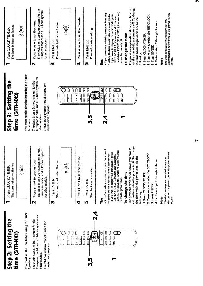
STR-NX1/NX3
SERVICE MANUAL
US Model
Canadian Model
AEP Model
UK Model
E Model
Australian Model
Tourist Model
STR-NX1/NX3 are the |
|
Tuner and Amplifier |
|
Section in HMC-NX1/NX3AV. |
Photo: STR-NX3 E model |
SPECIFICATIONS
– Continued on next page –
TUNER/AMPLIFIER
MICROFILM

|
TABLE OF CONTENTS |
|
1. |
SERVICING NOTES ............................................... |
3 |
2. |
GENERAL ................................................................... |
4 |
3. |
DISASSEMBLY ......................................................... |
6 |
4. |
TEST MODE .............................................................. |
8 |
5.DIAGRAMS
5-1. |
Note for Printed Wiring Boards and |
|
|
Schematic Diagrams ....................................................... |
11 |
5-2. |
Schematic Diagram – MAIN Board (1/3) – ................... |
12 |
5-3. |
Schematic Diagram – MAIN Board (2/3) – ................... |
13 |
5-4. |
Schematic Diagram – MAIN Board (3/3) – ................... |
14 |
5-5. |
Printed Wiring Board – MAIN Board – ........................ |
15 |
5-6. |
Printed Wiring Board – SURROUND AMP Board – ... |
16 |
5-7. |
Schematic Diagram – SURROUND AMP Board – ...... |
17 |
5-8. |
Printed Wiring Board – PA Board – .............................. |
18 |
5-9. |
Schematic Diagram – PA Board – ................................. |
19 |
5-10. |
Printed Wiring Boards – PANEL Section – .................. |
20 |
5-11. |
Schematic Diagram – PANEL Section – ....................... |
21 |
5-12. |
Printed Wiring Boards |
|
|
– TRANSFORMER Section – ........................................ |
22 |
5-13. |
Schematic Diagram – TRANSFORMER Section – ...... |
23 |
5-14. IC Pin Function Description ........................................... |
24 |
|
6. |
EXPLODED VIEWS ................................................ |
26 |
7. |
ELECTRICAL PARTS LIST ............................... |
30 |
SAFETY-RELATED COMPONENT WARNING!!
COMPONENTS IDENTIFIED BY MARK 0 OR DOTTED LINE WITH MARK 0 ON THE SCHEMATIC DIAGRAMS
AND IN THE PARTS LIST ARE CRITICAL TO SAFE OPERATION. REPLACE THESE COMPONENTS WITH SONY PARTS WHOSE PART NUMBERS APPEAR AS SHOWN IN THIS MANUAL OR IN SUPPLEMENTS PUBLISHED BY SONY.
ATTENTION AU COMPOSANT AYANT RAPPORT À LA SÉCURITÉ!
LES COMPOSANTS IDENTIFIÉS PAR UNE MARQUE 0
SUR LES DIAGRAMMES SCHÉMATIQUES ET LA LISTE DES PIÈCES SONT CRITIQUES POUR LA SÉCURITÉ DE FONCTIONNEMENT. NE REMPLACER CES COMPOSANTS QUE PAR DES PIÈCES SONY DONT LES NUMÉROS SONT DONNÉS DANS CE MANUEL OU DANS LES SUPPLÉMENTS PUBLIÉS PAR SONY.
2

SECTION 1
SERVICING NOTES
SAFETY CHECK-OUT
After correcting the original service problem, perform the following safety check before releasing the set to the customer:
Check the antenna terminals, metal trim, “metallized” knobs, screws, and all other exposed metal parts for AC leakage. Check leakage as described below.
LEAKAGE TEST
The AC leakage from any exposed metal part to earth ground and from all exposed metal parts to any exposed metal part having a return to chassis, must not exceed 0.5 mA (500 microamperes). Leakage current can be measured by any one of three methods.
1.A commercial leakage tester, such as the Simpson 229 or RCA WT-540A. Follow the manufacturers’ instructions to use these instruments.
2.A battery-operated AC milliammeter. The Data Precision 245 digital multimeter is suitable for this job.
3.Measuring the voltage drop across a resistor by means of a VOM or battery-operated AC voltmeter. The “limit” indication is 0.75 V, so analog meters must have an accurate lowvoltage scale. The Simpson 250 and Sanwa SH-63Trd are examples of a passive VOM that is suitable. Nearly all battery operated digital multimeters that have a 2 V AC range are suitable. (See Fig. A)
To Exposed Metal
Parts on Set
0.15 F |
|
|
|
1.5 kΩ |
AC |
|
|
|
voltmeter |
||
|
|
|
|
|
(0.75 V) |
|
|
|
|
|
|
• MODEL IDENTIFICATION
– Rear Panel –
PART No.
MODEL |
PART No. |
|
|
|
|
NX1: AEP, UK and Korean models |
4-221-391-0[] |
|
|
|
|
NX1: US and Canadian models |
4-221-391-1[] |
|
NX1: Malaysia, Singapore, Thai and |
4-221-391-2[] |
|
Tourist models |
||
|
||
NX3: AEP, UK, Korean and Australian models |
4-221-391-3[] |
|
NX3: US and Canadian models |
4-221-391-4[] |
|
|
|
|
NX3: Malaysia and Singapore models |
4-221-391-5[] |
Earth Ground
Fig. A. Using an AC voltmeter to check AC leakage.
3

• LOCATION OF CONTROLS
– Front Panel –
8 q; qs qf qh
7 9 qa qd qg qj
1
2
3
4
5
6
wf wg wh wj wk wl e;
– Rear Panel –
1 2
3
4
5
6
7
8
q; |
qa qs |
SECTION 2
GENERAL
|
|
|
1 |
TIMER indicator (US, Canadian, AEP and UK models) |
|
|
|
2 |
DISPLAY button |
|
|
|
3 |
?/1 button and indicator |
|
|
|
4 |
POWER SAVE/DEMO (STANDBY) button |
|
|
|
5 |
–m button |
|
|
|
6 |
+ M button |
|
qk |
7 |
FILE SELECT button |
|
|
8 VIDEO/DVD button |
|||
|
ql |
|||
|
||||
|
|
w; |
9 |
EDIT button |
|
|
|||
|
|
|
||
|
|
q; MD button |
|
|
|
qa REPEAT button |
|
|
|
qs TAPE button |
|
wa |
qd PLAY MODE button |
||
qf CD button |
|||
|
|
||
|
|
qg DBFB button |
|
|
ws |
qh TUNER button |
|
|
|||
|
|
||
|
wd |
qj DSP button |
|
|
qk TUNER BAND button |
||
|
|
||
|
|
ql STEREO/MONO button |
|
|
|
w; TUNER MEMORY button |
|
|
|
wa GROOVE button and indicator |
|
|
|
ws MIC LEVEL knob |
|
|
|
wd MIC jack |
|
|
|
wf PHONES jack |
|
|
|
wg Remote sensor |
|
|
|
wh Jog dial |
|
|
|
wj ENTER button and indicator |
|
|
|
wk DVD 5.1CH button and indicator (STR-NX3) |
|
|
|
wl PRO LOGIC button and indicator (STR-NX3) |
|
|
|
e; VOLUME knob |
|
1 AM ANTENNA terminals
2 FM ANTENNA terminal
3 SYSTEM CONTROL connector
4 VIDEO (AUDIO) IN jacks
5 MD IN jacks
96 MD OUT jacks
7 DVD 5.1CH INPUT jacks (STR-NX3)
8 SUPER WOOFER OUT jack
9 VOLTAGE SELECTOR switch (Malaysia, Singapore and Tourist models)
q; FRONT SPEAKER terminals qa REAR SPEAKER terminals
qs CENTER SPEAKER terminals (STR-NX3)
4
This section is extracted from instruction manual.
5

SECTION 3
DISASSEMBLY
Note: Follow the disassembly procedure in the numerical order given.
CASE
2 screw
(BVTP3 × 10)
3 case
1two screws (case 3 TP2)
1 two screws (case 3 TP2)
FRONT PANEL ASS’Y
1flat wire (CN132)
4 front panel ass’y
3 claw
1 flat wire (CN131)
2 two screws |
3 claw |
(BVTT3 × 6) |
6

BACK PANEL ASS’Y
2 connector (CN173)
1 flat wire (CN1)
5 back panel ass’y
3 seven screws (BVTP3 × 10)
4 claw
3 four screws |
|
|
(BVTP3 |
× 10) |
4 claw |
|
|
|
MAIN BOARD
1 connector (CN111)
1 two connectors (CN161, 181)
2 two screws (BVTP3 × 10)
3 connector (CN152)
4 main board
7

SECTION 4 TEST MODE
[CD Delivery Mode]
•Execute only if connected to the HTC-NX1.
•This mode moves the optical pick-up to the position durable to vibration. Use this mode when returning the set to the customer after repair.
Procedure:
1.Press the ?/1 button to turn the power ON.
2.Press the [ENTER] and ?/1 buttons simultaneously.
3.A message “LOCK” is displayed on the liquid crystal display, and the CD delivery mode is set.
[Change-over the MW Tuning Interval] (EXCEPT AEP and UK models)
• The MW tuning interval can be changed over 9 kHz or 10 kHz.
Procedure:
1.Press the ?/1 button to turn the power ON.
2.Press the [TUNER] button to select the function “TUNER”, and press the [TUNERBAND] button to select the BAND “MW”.
3.Press the ?/1 button to turn the power OFF.
4.Press the [TUNER MEMORY] and ?/1 buttons simultaneously, and the display on the liquid crystal display changes to “MW 9 k STEP” or “MW 10 k STEP”, and thus the tuning interval is changed over.
[MC Cold Reset]
• The cold reset clears all data including preset data stored in the RAM to initial conditions. Execute this mode when returning the set to the customer.
Procedure:
1.Turn the power ON or set to the DEMO mode.
2.Press the [GROOVE] and ?/1 buttons simultaneously.
3.The set is reset, and displays “COLD RESET”, then becomes DEMO mode.
[Amplifier Test Mode]
Procedure:
1.Press the ?/1 button to turn the power ON.
2.Press three buttons of [ENTER] , [DISPLAY] , and [TUNER BAND] simultaneously.
3.“ALC OFF” is displayed, then the function which was set before the test mode became active is displayed.
[LED and Liquid Crystal Display All Lit, Software Version Display, Key Check, VACS Level Display Mode]
Procedure:
1.Press the ?/1 button to turn the power ON.
2.Press three buttons of [ENTER] , [DISPLAY] , and [STEREO/MONO] simultaneously.
3.LEDs and liquid crystal display are all turned on.
Rotating the JOG dial changes over the check patterns of liquid crystal display.
4.Successively, the following three modes can be activated.
(1) Press the [VIDEO/DVD] button, and the software version is
displayed on the liquid crystal display.
(2)Press the [MD] button, and the key check mode is activated. In the key check mode, the liquid crystal display displays “K 0 J0 V0”. Each time a button is pressed, “K” value increases. However, once a button is pressed, it is no longer taken into account.
“J” value increases like 1, 2, 3 ... if turn the JOG dial clockwise, or it decreases like 0, 9, 8 ... if turn the JOG dial counterclockwise.
“V” value increases like 1, 2, 3 ... if turn the [VOLUME] dial clockwise, or it decreases like 0, 9, 8 ... if turn the JOG dial counterclockwise.
(3)Press the [TAPE] button, and the VACS level is displayed on the liquid crystal display.
5.To release from these mode, press three buttons in the same manner as step 2, or remove the power cord.
[MC Hot Reset]
• This mode resets the set with the preset data kept stored in the memory. The hot reset mode functions same as if the power cord is plugged in and out.
Procedure:
1.Turn the power ON or set to the DEMO mode.
2.Press three buttons of [ENTER] , [DISPLAY] , and [TUNER MEMORY] simultaneously.
3.The set is reset, and becomes standby state.
[Change-over of VACS ON/OFF]
Procedure:
1.Press the ?/1 button to turn the power ON.
2.Press three buttons of [ENTER] , [DISPLAY] , and [GROOVE] simultaneously, and the display on the liquid crystal display changes to “VACS ON” or “VACS OFF”, and thus the VACS ON/OFF is changed over.
[VIDEO input, Record and CD play in CD function]
• Execute only if connected to the HTC-NX1.
Procedure:
1. |
Press the |
?/1 |
button to turn the power ON. |
||
2. |
Press three buttons of [ENTER] , [DISPLAY] , and |
||||
|
|
- m |
simultaneously. |
||
3.“DVD 5.1CH” is displayed on liquid crystal display, and at the same time, CD is played and the deck B is placed in the record status.
[CD Service Mode]
•Execute only if connected to the HTC-NX1.
•This mode can run the CD sled motor optionally. Use this mode, for instance, when cleaning the optical pick-up.
Procedure:
1.Press the ?/1 button to turn the power ON.
2.Press the [CD] button to select the function “CD”.
3.Press three buttons of [ENTER] , [POWER SAVE/DEMO] , and [STEREO/MONO] simultaneously.
4.Set to the Sled Servo mode.
5.With the CD in stop status, turn the JOG dial clockwise to move the optical pick-up to outside track, or turn it counterclockwise to inside track.
6.To release from this mode, perform as follows.
1)Move the optical pick-up to the most inside track.
2)Remove the power cord.
Notes: • Always move the optical pick-up to most inside track when releasing from this mode. Otherwise, a disc will not be unloaded.
• Do not run the sled motor excessively, otherwise the gear can be chipped.
8

[Aging Mode]
• Execute only if connected to the HTC-NX1.
This mode can be used for operation check of CD section and tape deck section.
CD section and tape deck section work in parallel.
• If an error occurred:
The aging operation stops only an error occurred sections and display then status.
• If no error occurs:
The aging operation continues repeatedly.
Procedure:
1.Set disc in DISC5 tray.
2.Load the tapes into the decks A and B respectively.
3.Press the [PLAY MODE] button to set the “ALL DISCS” mode, and press the [REPEAT] button to “REPEAT” off.
4.Press the [CD] button to select the function “CD”.
5.Press three buttons of [ENTER] , [POWER SAVE/DEMO] , and [TUNER BAND] simultaneously.
6.The aging mode is activated, if the indicator of disc tray number on the liquid crystal display is blinking.
7.To release from the aging mode, press the ?/1 button to turn the power OFF and operate the cold reset. (Refer to the “MC Cold Reset”)
1. Display at the Aging Mode
•Display operating state of CD section and tape deck section alternately.
•If an error occurred, stop display which that section.
2. CD Section
•Display at the aging mode is the same as the normal operation.
•The sequence during the aging mode is following as below.
Aging mode sequence (CD section) :
Open the disc1 tray
Disc5 chucking
Disc5 TOC read
Disc5 play track1 for 2 seconds
Disc5 play last track for 2 seconds
• Display at an error occurred 1) Display of the error count
(1)Press three buttons of [ENTER] , [POWER SAVE/DEMO] , and [GROOVE] simultaneously.
(2)Display of the error count following as below.
Display
EMC**EDC**
Notes:
EMC**: The number of mechanical error.
EDC** : The number of no disc error after chucking the disc.
2) Display of mechanical error
Display
E**M##$$&&
Notes:
**: The number of mechanical error.(“00” is latest one)
(Press the [PLAY MODE] button to changes next error display) ## : Not used.
$$ : Loading error. (Second figure is not used)
D : The error in the midst of close at the except mechanical trouble. E : The error in the midst of open at the except mechanical trouble. C : The error in the midst of chuck up at the except mechanical
trouble.
F : The error in the midst of EX-open at the except mechanical trouble.
&&: Loading error. (Second figure in not used) 1:The error in the midst of chuck up. 2:The error in the midst of chuck down. 3:Time up of EX-open
4:Time up of EX-close.
3) Display of no disc error
Display
E**D##$$&&
Notes:
**: The number of mechanical error.(“00” is latest one)
(Press the [REPEAT] button to changes next error display)
##:
01: Focus error 02: GFS error 03: Set up error
$$:
00: No disc error when does not chucking retry.
02: No disc error when chucking retry to completion.
&&: The state when judged no disc error. (Second figure is not used) 1:Stop
2:Set up 3:TOC read 4:Access 5:Play 6:Pause
7:Manual search (Play)
8:Manual search (Pause)3. Tape Deck Section
9
3. Tape Deck Section
•The sequence during the aging mode is following as below.
•If an error occurred, stop display that step.
Aging mode sequence (Tape deck section) :
Rewind the tape A and B
“TAPE A AG-1”
Shut off
FWD play the tape A
“TAPE A AG-2”
2 minutes
Fast forward the tape A
“TAPE A AG-3”
Shut off or 20 seconds
REV play the tape A
“TAPE A AG-4”
2 minutes
Rewind the tape A
“TAPE A AG-5”
Shut off
FWD play the tape B
“TAPE B AG-2”
2 minutes
Fast forward the tape B
“TAPE B AG-3”
Shut off or 20 seconds
REV play the tape B
“TAPE A AG-4”
2 minutes
Rewind the tape B
“TAPE B AG-5”
Shut off
Note: “TAPE * AG-*” is display of each step.
10

SECTION 5
DIAGRAMS
5-1. NOTE FOR PRINTED WIRING BOARDS AND SCHEMATIC DIAGRAMS
Note on Printed Wiring Board:
•X : parts extracted from the component side.
•Y : parts extracted from the conductor side.
•x : parts mounted on the conductor side.
•b: Pattern from the side which enables seeing.
(The other layers' patterns are not indicated)
•Indication of transistor.
Q
B C E
These are omitted.
Q
B C E
These are omitted.
Note on Schematic Diagram:
•All capacitors are in µF unless otherwise noted. pF: µµF 50 WV or less are not indicated except for electrolytics and tantalums.
•All resistors are in Ω and 1/4 W or less unless otherwise specified.
•f : internal component.
•2: nonflammable resistor.
•5: fusible resistor.
•C : panel designation.
Note: |
Note: |
The components identi- |
Les composants identifiés par |
fied by mark 0or dotted |
une marque 0sont critiques |
line with mark 0are criti- |
pour la sécurité. |
cal for safety. |
Ne les remplacer que par une |
Replace only with part |
pièce portant le numéro |
number specified. |
spécifié. |
|
|
•U : B+ Line.
•V : B– Line.
•Voltages and waveforms are dc with respect to ground under no-signal (detuned) conditions.
no mark : TUNER (FM)
•Voltages are taken with a VOM (Input impedance 10 MΩ). Voltage variations may be noted due to normal production tolerances.
•Waveforms are taken with a oscilloscope.
Voltage variations may be noted due to normal production tolerances.
•Circled numbers refer to waveforms.
•Signal path.
F : TUNER (FM)
E : TAPE PLAYBACK G : RECORD
J : CD PLAY
N : MIC INPUT
•Abbreviation
AUS |
: Australian model |
MY |
: Malaysia model |
CND |
: Canadian model |
SP |
: Singapore model |
JE |
: Tourist model |
TH |
: Thai model |
KR |
: Korean model |
|
|
• Circuit Boards Location
SUB TRANS board
(US, Canadian, AEP, UK)
TRANS board
BACK LIGHT board
PANEL baord
R board
• IC Block Diagram
– MAIN Board –
IC401 |
|
BA3830F |
|
|
|
|
|
|
REFERENCE |
RESET |
18 |
RESET |
|
R02 |
1 |
|
|
|
||
CURRENT |
|
|
|
|||
|
|
|
|
|
||
R01 |
2 |
REFERENCE |
|
|
|
|
CURRENT |
|
|
|
|||
|
|
|
|
|
||
LINE NF |
3 |
|
|
17 |
F01 |
|
|
|
16 |
F02 |
|||
LINE IN |
4 |
– |
BAND |
|||
15 |
F03 |
|||||
|
|
+ |
PASS |
14 |
F04 |
|
|
|
|
FILTER |
|||
|
|
|
13 |
F05 |
||
|
|
|
DET |
|||
|
|
|
12 |
F06 |
||
|
|
|
|
|||
REC NF |
5 |
|
|
|
|
|
REC IN |
6 |
– |
|
11 |
REC LEVEL |
|
|
|
+ |
|
|||
|
|
|
|
|
||
|
|
|
|
10 |
VCC |
|
RESET C |
7 |
|
|
|
|
|
BIAS C |
8 |
|
|
|
|
|
GND |
9 |
|
|
|
|
• Waveforms
– MAIN Board –
1 IC501 q; (XCIN)
1.4 Vp-p
32.768 kHz
2 IC501 qd (XOUT)
3 Vp-p
16 MHz
TUNER pack
SURROUND AMP board (NX3)
MAIN board
PA board
11 11
STR-NX1/NX3
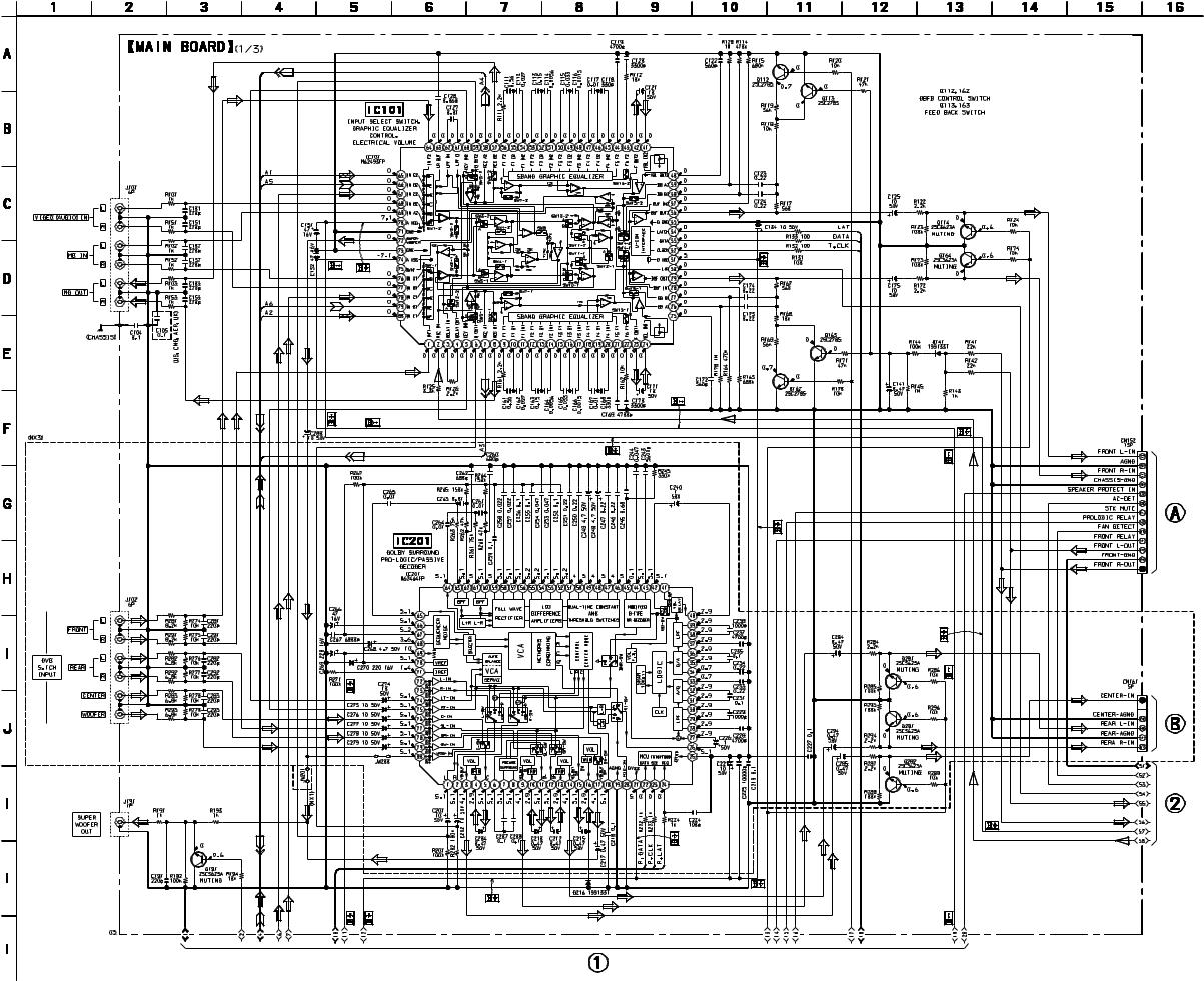
5-2. SCHEMATIC DIAGRAM – MAIN Board (1/3) –
(Page
19)
(Page
17)
(Page
14)
(Page 13)
12 12

STR-NX1/NX3
5-3. SCHEMATIC DIAGRAM – MAIN Board (2/3) – See• page 11 for Waveforms.
(Page 12) |
|
(Page 23) |
|
|
(Page 14) |
13 |
13 |

STR-NX1/NX3
5-4. SCHEMATIC DIAGRAM – MAIN Board (3/3) – See• page 11 for IC Block Diagram.
(Page 12) |
(Page 21) |
|
|
(Page 13) |
|
|
(Page 23) |
|
(Page 23) |
|
(Page 21) |
14 |
14 |
• Semiconductor Location
Ref. No. |
Location |
|
Ref. No. |
Location |
|
|
|
|
|
D141 |
A-8 |
|
IC921 |
C-2 |
D216 |
E-9 |
|
Q112 |
A-8 |
D501 |
B-2 |
|
||
D502 |
D-1 |
|
Q113 |
A-8 |
D503 |
D-1 |
|
Q114 |
G-6 |
D504 |
E-1 |
|
Q162 |
A-9 |
D505 |
E-1 |
|
Q163 |
A-9 |
D506 |
E-1 |
|
Q164 |
G-6 |
D507 |
F-1 |
|
Q191 |
G-11 |
D508 |
E-2 |
|
Q281 |
D-8 |
D510 |
C-1 |
|
Q282 |
D-7 |
D901 |
B-5 |
|
Q291 |
D-8 |
D902 |
A-5 |
|
Q411 |
D-5 |
D903 |
B-5 |
|
Q421 |
C-3 |
D904 |
A-4 |
|
Q431 |
E-6 |
D905 |
A-6 |
|
Q432 |
D-6 |
D906 |
A-6 |
|
Q461 |
D-5 |
D914 |
A-3 |
|
Q501 |
F-1 |
D915 |
B-3 |
|
Q502 |
F-1 |
D920 |
B-4 |
|
Q503 |
F-1 |
D921 |
B-3 |
|
Q901 |
A-6 |
D922 |
E-7 |
|
Q902 |
A-6 |
D923 |
E-7 |
|
Q903 |
A-6 |
D924 |
D-6 |
|
Q904 |
A-3 |
D925 |
B-4 |
|
Q905 |
A-3 |
D931 |
A-4 |
|
Q906 |
B-3 |
D932 |
A-4 |
|
Q907 |
B-4 |
|
|
|
Q921 |
B-3 |
IC101 |
B-9 |
|
Q923 |
C-3 |
IC201 |
E-9 |
|
Q924 |
B-3 |
IC401 |
E-5 |
|
Q951 |
B-6 |
IC501 |
E-3 |
|
Q952 |
B-6 |
IC502 |
E-1 |
|
Q953 |
B-6 |
IC901 |
A-2 |
|
|
|
|
|
|
|
|

STR-NX1/NX3
5-5. PRINTED WIRING BOARD – MAIN Board – See• page 11 for Circuit Boards Location.
(Page 22)
(Page 22)
(Page
20)
(Page 22)
(Page
20)
(Page 16)
(Page 18)
15 15

STR-NX1/NX3
5-6. PRINTED WIRING BOARD – SURROUND AMP Board – See• page 11 for Circuit Boards Location.
• Semiconductor
Location
Ref. No. |
Location |
|
|
D101 |
C-2 |
D102 |
C-3 |
D151 |
C-2 |
D191 |
C-2 |
IC101 |
A-2 |
Q101 |
B-3 |
Q103 |
A-3 |
Q104 |
A-3 |
Q151 |
B-2 |
Q181 |
C-1 |
|
|
(Page 15)
(Page 18)
16 16

STR-NX1/NX3
5-7. SCHEMATIC DIAGRAM – SURROUND AMP Board –
(NX3) |
(Page 12) |
(Page 19) |
The components identified by |
Les composants identifiés par une |
mark 0 or dotted line with |
marque 0 sont critiques pour la |
mark 0are critical for safety. |
sécurité. |
Replace only with part numNe les remplacer que par une pièce |
|
ber specified. |
portant le numéro spécifié. |
17 17

STR-NX1/NX3
5-8. PRINTED WIRING BOARD – PA Board – See• page 11 for Circuit Boards Location.
(Page 15)
(Page
16)
(Page 22)
• Semiconductor Location
Ref. No. |
Location |
|
Ref. No. |
Location |
|
Ref. No. |
Location |
|
|
|
|
|
|
|
|
D802 |
B-5 |
|
IC801 |
C-8 |
|
Q829 |
G-4 |
D821 |
E-4 |
|
Q801 |
B-5 |
|
Q830 |
G-4 |
D831 |
C-6 |
|
|
Q831 |
C-7 |
||
D852 |
C-5 |
|
Q821 |
D-7 |
|
Q851 |
C-5 |
D871 |
B-10 |
|
Q822 |
D-7 |
|
Q881 |
B-10 |
D881 |
E-2 |
|
Q823 |
C-7 |
|
Q882 |
B-9 |
D882 |
H-2 |
|
Q824 |
C-7 |
|
Q883 |
C-9 |
D883 |
A-11 |
|
Q825 |
H-4 |
|
Q884 |
C-9 |
D884 |
C-11 |
|
Q826 |
H-4 |
|
Q885 |
D-9 |
D885 |
F-10 |
|
Q827 |
H-4 |
|
Q886 |
D-9 |
|
|
|
Q828 |
G-4 |
|
|
|
|
|
|
|
|
|
|
|
18 18

5-9. SCHEMATIC DIAGRAM – PA Board –
The components identified by |
Les composants identifiés par une |
mark 0 or dotted line with |
marque 0 sont critiques pour la |
mark 0are critical for safety. |
sécurité. |
Replace only with part num- |
Ne les remplacer que par une pièce |
ber specified. |
portant le numéro spécifié. |
|
|
STR-NX1/NX3
(Page 23)
(Page 12)
(Page
17)
19 19
STR-NX1/NX3
5-10. PRINTED WIRING BOARDS – PANEL Section – See• page 11 for Circuit Boards Location.
(Page 15)
• Semiconductor
Location
Ref. No. |
Location |
|
|
||||||||||||
D631 |
E-2 |
|
|||||||||||||
D632 |
F-4 |
|
|||||||||||||
D633 |
F-4 |
|
|||||||||||||
D636 |
G-5 |
|
|||||||||||||
D637 |
A-7 |
|
|||||||||||||
|
|||||||||||||||
D638 |
D-7 |
|
|||||||||||||
|
|||||||||||||||
D643 |
C-6 |
|
|||||||||||||
D644 |
C-7 |
|
|||||||||||||
D645 |
C-4 |
|
|||||||||||||
|
|||||||||||||||
D646 |
C-5 |
|
|||||||||||||
D647 |
C-2 |
|
|||||||||||||
D648 |
C-3 |
|
|||||||||||||
IC701 |
F-2 |
|
|||||||||||||
Q631 |
E-1 |
|
|
|
|
|
|||||||||
|
|
|
|||||||||||||
Q632 |
F-3 |
|
|
|
|
|
|
|
|
|
|||||
Q633 |
E-3 |
|
|
|
|
|
|||||||||
|
|
|
|||||||||||||
Q636 |
F-5 |
|
|
|
|
|
|||||||||
Q637 |
B-7 |
|
|||||||||||||
Q638 |
D-7 |
|
|||||||||||||
Q641 |
D-7 |
|
|||||||||||||
Q642 |
D-7 |
|
|||||||||||||
Q643 |
D-7 |
|
|||||||||||||
(Page 15)
20 20

STR-NX1/NX3
5-11. SCHEMATIC DIAGRAM – PANEL Section –
(Page 14)
(Page 14)
21 21

STR-NX1/NX3
5-12. PRINTED WIRING BOARDS – TRANSFORMER Section – See• page 11 for Circuit Boards Location.
 (MY, SP, JE / NX3:US, CND)
(NX1:US, CND)
JW953
(Page 15)
• Semiconductor
Location
Ref. No. |
Location |
|
|
D952 |
A-4 |
D953 |
A-5 |
D954 |
A-4 |
D955 |
A-5 |
D956 |
B-4 |
D957 |
A-3 |
IC991 |
A-3 |
Q991 |
A-3 |
|
|
(Page 15)
(Page 15)
(Page 18)
22 22

STR-NX1/NX3
5-13. SCHEMATIC DIAGRAM – TRANSFORMER Section –
(Page 19)
(Page 14)
(Page 13)
(Page 14)
The components identified by |
Les composants identifiés par une |
mark 0 or dotted line with |
marque 0 sont critiques pour la |
mark 0are critical for safety. |
sécurité. |
Replace only with part num- |
Ne les remplacer que par une pièce |
ber specified. |
portant le numéro spécifié. |
|
|
23 23

5-14. IC PIN FUNCTION DESCRIPTION
• MAIN BOARD IC501 M30622MA-A12FP (SYSTEM CONTROLLER )
Pin No. |
Pin Name |
I/O |
|
Description |
|
|
||
|
|
|
|
|||||
1 |
L+R |
I |
Spectrum analyzer drive signal input from the spectrum analyzer band-pass filter (IC401) |
|||||
(for VACS, non-stop signal) |
|
|
|
|
||||
|
|
|
|
|
|
|
||
|
|
|
|
|||||
2 |
BPF SL |
I |
Spectrum analyzer drive (super low frequency) signal input from the spectrum analyzer band-pass |
|||||
filter (IC401) (for 40 Hz) |
|
|
|
|
||||
|
|
|
|
|
|
|
||
|
|
|
|
|
||||
3 |
F RELAY |
O |
Speaker protect relay drive signal output for the front side speaker |
“H”: relay on |
||||
|
|
|
|
|
||||
4 |
R RELAY |
O |
Speaker protect relay drive signal output for the rear side speaker |
“H”: relay on |
||||
|
|
|
|
|||||
5 |
SIRCS |
I |
Remote control signal input from the remote control receiver (IC601) |
|||||
|
|
|
|
|
||||
6 |
LINE MUTE |
O |
Line muting on/off control signal output terminal “L”: muting on |
|
||||
7 |
DBFB |
O |
DBFB normal/high selection signal output to the M62493FP (IC101) |
|||||
“L”: DBFB high, “H”: DBFB low/off |
|
|
|
|
||||
|
|
|
|
|
|
|
||
|
|
|
|
|
||||
8 |
BYTE |
I |
External data bus line byte selection signal input terminal |
Fixed at “L” in this set |
||||
|
|
|
|
|
|
|
|
|
9 |
CNVSS |
— |
Ground terminal |
|
|
|
|
|
|
|
|
|
|
|
|
||
10 |
XCIN |
I |
Sub system clock input terminal (32.768 kHz) |
|
|
|
||
|
|
|
|
|
|
|||
11 |
XCOUT |
O |
Sub system clock output terminal (32.768 kHz) |
|
|
|||
|
|
|
|
|
||||
12 |
RESET |
I |
System reset signal input from the reset signal generator (IC502) |
“L”: reset |
||||
For several hundreds msec. after the power supply rises, “L” is input, then it changes to “H” |
||||||||
|
|
|
||||||
|
|
|
|
|
|
|
||
13 |
XOUT |
O |
Main system clock output terminal (16 MHz) |
|
|
|
||
|
|
|
|
|
|
|
|
|
14 |
VSS |
— |
Ground terminal |
|
|
|
|
|
|
|
|
|
|
|
|
||
15 |
XIN |
I |
Main system clock input terminal (16 MHz) |
|
|
|
||
|
|
|
|
|
|
|
|
|
16 |
VCC |
— |
Power supply terminal (+5V) |
|
|
|
|
|
|
|
|
|
|
|
|||
17 |
NMI |
I |
Non-maskable interrupt input terminal |
Fixed at “H” in this set |
|
|||
|
|
|
|
|||||
18 |
WAKE UP |
O |
Wakeup control signal output to the CPU on the HTC-NX1 “H” active |
|||||
|
|
|
|
|
||||
19 |
PHONES MUTE |
O |
Muting on/off control signal output terminal |
“L”: muting on Not used (open) |
||||
|
|
|
|
|
||||
20 |
RDS INT |
I |
RDS serial data transfer clock signal input from the tuner pack |
|
||||
(Used for the AEP and UK models only) |
|
|
|
|||||
|
|
|
|
|
|
|||
|
|
|
|
|||||
21 |
RDS DATA |
I |
RDS serial data input from the tuner pack (Used for the AEP and UK models only) |
|||||
|
|
|
|
|||||
22 |
AC CUT |
I |
AC off detection signal input from the reset signal generator (IC502) “L”: AC cut checked |
|||||
|
|
|
|
|
||||
23 |
PL CLK |
O |
Serial data transfer clock signal output to the M62464FP (IC201) |
|
||||
(Used for the STR-NX3 only) |
|
|
|
|
||||
|
|
|
|
|
|
|
||
|
|
|
|
|
||||
24 |
PL DATA |
O |
Serial data output to the M62464FP (IC201) |
(Used for the STR-NX3 only) |
||||
|
|
|
|
|
||||
25 |
PL LAT |
O |
Serial data latch pulse output to the M62464FP (IC201) |
(Used for the STR-NX3 only) |
||||
|
|
|
|
|
||||
26 |
STK POWER |
O |
Power amplifier on/off selection signal output terminal |
“L”: standby mode, “H”: on |
||||
|
|
|
|
|||||
27 |
SPEAKER |
I |
Protect on/off detection signal input from the speaker protect circuit |
|||||
PROTECT |
“L”: protect on, “H”: protect off |
|
|
|
|
|||
|
|
|
|
|
|
|||
|
|
|
|
|
|
|
||
28 |
SOFT-TEST |
O |
Output terminal for the software test |
Not used (open) |
|
|
||
|
|
|
|
|||||
29 |
IIC CLK |
I/O |
Communication data reading clock signal input or transfer clock signal output with the CPU on |
|||||
the HTC-NX1 |
|
|
|
|
||||
|
|
|
|
|
|
|
||
|
|
|
|
|
|
|||
30 |
IIC DATA |
I/O |
Communication data bus with the CPU on the HTC-NX1 |
|
|
|||
|
|
|
|
|
|
|
|
|
31 |
TXD1 |
O |
Not used (open) |
|
|
|
|
|
|
|
|
|
|
|
|
|
|
32 |
RXD1 |
I |
Not used (fixed at “L”) |
|
|
|
|
|
|
|
|
|
|
|
|
|
|
33 |
CLK1 |
I |
Not used (fixed at “L”) |
|
|
|
|
|
|
|
|
|
|
|
|
|
|
34 |
RTS1 |
O |
Not used (open) |
|
|
|
|
|
35 |
LCD DATA |
O |
Serial data output to the liquid crystal display unit (LCD601) |
|
||||
|
|
|
|
|
|
|
|
|
36 |
RXD0 |
I |
Not used (fixed at “L”) |
|
|
|
|
|
|
|
|
|
|||||
37 |
LCD CLK |
O |
Serial data transfer clock signal output to the liquid crystal display unit (LCD601) |
|||||
|
|
|
|
|
|
|||
38 |
493 LT |
O |
Serial data latch pulse output to the M62493FP (IC101) |
|
|
|||
|
|
|
|
|
|
|
|
|
Pin No. |
Pin Name |
I/O |
|
Description |
|
|
|||
|
|
|
|
|
|||||
39 |
CLOCK OUT |
O |
Output terminal for the clock signal check Not used (open) |
|
|||||
|
|
|
|
|
|||||
40 |
VC L+R/L–R |
O |
Virtual cinema L+R/L–R selection signal output terminal |
Not used (open) |
|||||
|
|
|
|
|
|
|
|
|
|
41 |
XHOLD |
I |
Not used (fixed at “L”) |
|
|
|
|
|
|
|
|
|
|
|
|||||
42 |
LCD SW |
O |
Liquid crystal display on/off selection signal output terminal |
“L”: on, “H”: off |
|||||
Not used (open) |
|
|
|
|
|
||||
|
|
|
|
|
|
|
|
||
|
|
|
|
|
|||||
43 |
STBY RELAY |
O |
Main power on/off control signal output terminal |
“L”: standby mode, “H”: power on |
|||||
(Used for the US, Canadian, AEP and UK models only) |
|
|
|||||||
|
|
|
|
|
|||||
|
|
|
|
||||||
44 |
BASS FREQ |
O |
Sync bass frequency normal/high selection signal output to the M62493FP (IC101) |
||||||
“L”: sync bass off (normal), “H”: sync bass high |
Not used (open) |
||||||||
|
|
|
|||||||
|
|
|
|
|
|
|
|
|
|
45 |
OPT SEL |
O |
Not used (open) |
|
|
|
|
|
|
|
|
|
|
|
|
|
|
|
|
46 |
XWR |
I |
Not used (fixed at “H”) |
|
|
|
|
|
|
|
|
|
|
|
|
|
|
||
47 |
493 DATA |
O |
Serial data output to the M62493FP (IC101) |
|
|
|
|
||
|
|
|
|
||||||
48 |
493 CLK |
O |
Serial data transfer clock signal output to the M62493FP (IC101) |
||||||
|
|
|
|
|
|||||
49 |
ST MUTE |
O |
Tuner muting control signal output to the tuner pack |
“H”: muting on |
|||||
|
|
|
|
|
|||||
50 |
STEREO |
I |
FM stereo detection signal input from the tuner pack |
“L”: stereo |
|||||
|
|
|
|
|
|
||||
51 |
TUNED |
I |
Tuning detection signal input from the tuner pack |
“L”: tuned |
|
||||
|
|
|
|
|
|
|
|
||
52 |
ST CE |
O |
PLL chip enable signal output to the tuner pack |
|
|
|
|
||
|
|
|
|
|
|
|
|
||
53 |
ST DOUT |
O |
PLL serial data output to the tuner pack |
|
|
|
|
||
|
|
|
|
|
|
|
|
||
54 |
ST DIN |
I |
PLL serial data input from the tuner pack |
|
|
|
|
||
|
|
|
|
|
|||||
55 |
ST CLK |
O |
PLL serial data transfer clock signal output to the tuner pack |
|
|||||
|
|
|
|
|
|||||
56 |
VC BYPASS |
O |
Virtual cinema bypass control signal output terminal |
Not used (open) |
|||||
|
|
|
|
|
|||||
57 |
PHONES |
I |
Connection detect signal input of the headphone jack (J701) |
|
|||||
DETECT |
“L”: no connected, “H”: headphone connected |
|
|
|
|
||||
|
|
|
|
|
|
||||
|
|
|
|
||||||
58 |
LCD LAT |
O |
Serial data latch pulse output to the liquid crystal display unit (LCD601) |
||||||
|
|
|
|
||||||
59 |
LCD A0 |
O |
Address signal output to the liquid crystal display unit (LCD601) |
||||||
|
|
|
|
|
|||||
60 |
LCD RESET |
O |
Reset signal output to the liquid crystal display unit (LCD601) |
“L”: reset |
|||||
|
|
|
|
|
|
|
|
|
|
61 |
NC |
O |
Not used (open) |
|
|
|
|
|
|
|
|
|
|
|
|
|
|
|
|
62 |
VCC |
— |
Power supply terminal (+5V) |
|
|
|
|
|
|
|
|
|
|
|
|
|
|
|
|
63 |
NC |
O |
Not used (open) |
|
|
|
|
|
|
|
|
|
|
|
|
|
|
|
|
64 |
VSS |
— |
Ground terminal |
|
|
|
|
|
|
|
|
|
|
|
|
|
|
|
|
65 to 68 |
NC |
O |
Not used (open) |
|
|
|
|
|
|
|
|
|
|
||||||
69 |
JOG B |
I |
Jog dial pulse input from the rotary encoder (S652 JOG) (B phase input) |
||||||
|
|
|
|
||||||
70 |
JOG A |
I |
Jog dial pulse input from the rotary encoder (S652 JOG) (A phase input) |
||||||
|
|
|
|
||||||
71 |
VOL B |
I |
Jog dial pulse input from the rotary encoder (S651 VOLUME) (B phase input) |
||||||
|
|
|
|
||||||
72 |
VOL A |
I |
Jog dial pulse input from the rotary encoder (S651 VOLUME) (A phase input) |
||||||
|
|
|
|
|
|
|
|
|
|
73 to 78 |
NC |
O |
Not used (open) |
|
|
|
|
|
|
|
|
|
|
||||||
79 |
LED FUNCTION |
O |
LED drive signal output of the key illumination indicator (D643 to D648) “H”: LED on |
||||||
|
|
|
|
|
|||||
80 |
LED POWER |
O |
LED drive signal output of the I/1 indicator (D638) |
“H”: LED on |
|||||
|
|
|
|
|
|||||
81 |
LED TIMER |
O |
LED drive signal output of the TIMER indicator (D637) |
“H”: LED on |
|||||
(Used for the US, Canadian, AEP and UK models only) |
|
|
|||||||
|
|
|
|
|
|||||
|
|
|
|
||||||
82 |
LED LCD |
O |
LED drive signal output of the liquid crystal display back light indicator (D639 to D642) |
||||||
“H”: LED on |
|
|
|
|
|
||||
|
|
|
|
|
|
|
|
||
|
|
|
|
|
|||||
83 |
LED ENTER |
O |
LED drive signal output of the ENTER indicator (D636) |
“H”: LED on |
|||||
|
|
|
|
|
|
|
|
||
84 |
LED JOG |
O |
LED drive signal output terminal |
Not used (open) |
|
|
|
||
|
|
|
|
|
|
|
|
||
85 |
LED CINEMA |
O |
LED drive signal output terminal |
Not used (open) |
|
|
|
||
|
|
|
|
|
|||||
86 |
LED DOLBY |
O |
LED drive signal output of the PRO LOGIC indicator (D633) |
“H”: LED on |
|||||
(Used for the STR-NX3 only) |
|
|
|
|
|
||||
|
|
|
|
|
|
|
|
||
|
|
|
|
|
|
|
|
|
|
24 24
Pin No. |
Pin Name |
I/O |
Description |
|
|
|
|
|
|
|
|
87 |
LED 5.1CH |
O |
LED drive signal output of the DVD 5.1CH indicator (D632) |
“H”: LED on |
|
(Used for the STR-NX3 only) |
|
||||
|
|
|
|
||
|
|
|
|
|
|
88 |
LED GROOVE |
O |
LED drive signal output of the GROOVE indicator (D631) |
“H”: LED on |
|
|
|
|
|
||
89 |
BPF 1 |
I |
Spectrum analyzer drive (low frequency) signal input from the spectrum analyzer band-pass filter |
||
(IC401) (for 100 Hz) |
|
||||
|
|
|
|
||
|
|
|
|
||
90 |
BPF 2 |
I |
Spectrum analyzer drive (low and middle frequency) signal input from the spectrum analyzer |
||
band-pass filter (IC401) (for 400 Hz) |
|
||||
|
|
|
|
||
|
|
|
|
||
91 |
BPF 3 |
I |
Spectrum analyzer drive (middle and high frequency) signal input from the spectrum analyzer |
||
band-pass filter (IC401) (for 2 kHz) |
|
||||
|
|
|
|
||
|
|
|
|
||
92 |
BPF 4 |
I |
Spectrum analyzer drive (high frequency) signal input from the spectrum analyzer band-pass filter |
||
(IC401) (for 6 kHz) |
|
||||
|
|
|
|
||
|
|
|
|
|
|
|
|
|
Key input terminal (A/D input) |
|
|
93 |
KEY1 |
I |
S615 to S617, S619 to S624 (TUNER BAND, STEREO/MONO, TUNER MEMORY, |
||
GROOVE, + M, – m, ENTER, DVD 5.1CH, PRO LOGIC) keys input |
|||||
|
|
|
|||
|
|
|
(S623 DVD 5.1CH, S624 PRO LOGIC keys: used for the STR-NX3 only) |
||
|
|
|
|
|
|
94 |
KEY0 |
I |
Key input terminal (A/D input) |
|
|
S601 to S614 (I/1, DISPLAY, POWER SAVE/DEMO (STANDBY), VIDEO/DVD, MD, TAPE, |
|||||
|
|
|
CD, TUNER, DSB, DBFB, PLAY MODE, REPEAT, EDIT, FILE SELECT) keys input |
||
|
|
|
|
|
|
95 |
MODEL-IN |
I |
Destination setting terminal |
|
|
|
|
|
|
|
|
96 |
AVSS |
— |
Ground terminal (for A/D conversion) |
|
|
|
|
|
|
|
|
97 |
SPEC-IN |
I |
Setting terminal for the version |
|
|
|
|
|
|
|
|
98 |
VREF |
I |
Reference voltage (+5V) input terminal (for A/D conversion) |
|
|
|
|
|
|
|
|
99 |
AVCC |
— |
Power supply terminal (+5V) (for A/D conversion) |
|
|
|
|
|
|
||
100 |
POWER |
O |
Power on/off control signal output terminal “L”: standby mode, “H”: power on |
||
|
|
|
|
|
|
25

SECTION 6
EXPLODED VIEWS
NOTE:
•-XX and -X mean standardized parts, so they may have some difference from the original one.
•Color Indication of Appearance Parts
Example:
KNOB, BALANCE (WHITE) . . . (RED)
− |
− |
Parts Color |
Cabinet's Color |
•Items marked “*” are not stocked since they are seldom required for routine service. Some delay should be anticipated when ordering these items.
•The mechanical parts with no reference number in the exploded views are not supplied.
•Hardware (# mark) list is given in the last of the electrical parts list.
• Abbreviation |
|
|
|
AUS : Australian model |
MY |
: Malaysia model |
|
CND : Canadian model |
SP |
: Singapore model |
|
JE |
: Tourist model |
TH |
: Thai model |
KR |
: Korean model |
|
|
(1) |
GENERAL SECTION |
M401 |
|
|
|||
|
|
2 |
#1 |
|
|
|
|
|
|
|
6 |
1
4
1
5
Front panel ass’y
 #4
#4
The components identified by mark 0or dotted line with mark 0are critical for safety.
Replace only with part number specified.
Les composants identifiés par une marque 0sont critiquens pour la sécurité.
Ne les remplacer que par une pièce portant le numéro spécifié.
#1
#1
#1
 #1
#1
#1
3
Ref. No. |
Part No. |
Description |
Remark |
Ref. No. |
Part No. |
Description |
Remark |
1 |
3-363-099-11 |
SCREW (CASE 3 TP2) |
|
4 |
1-773-011-11 WIRE (FLAT TYPE) (15 CORE) |
|
|
2 |
4-221-365-11 |
CASE |
|
|
|
(AEP, UK, MY, SP, JE) |
|
3 |
X-4952-291-1 |
PANEL ASSY, BACK (NX1: AEP, UK, KR) |
5 |
4-965-822-01 FOOT |
|
||
3 |
X-4952-292-1 |
PANEL ASSY, BACK (NX1: US, CND) |
|
6 |
1-233-545-11 TUNER PACK (FM/AM) (NX1: TH, KR/NX3: KR, |
||
3 |
X-4952-293-1 |
PANEL ASSY, BACK (NX1: MY, SP, JE) |
|
|
|
|
AUS) |
|
|
|
|
6 |
1-233-546-11 TUNER PACK (FM/MW/SW) (MY, SP) |
|
|
3 |
X-4952-294-1 |
PANEL ASSY, BACK (NX3: AEP, UK) |
|
6 |
1-693-443-11 TUNER PACK (FM/AM) (AEP, UK) |
|
|
3 |
X-4952-295-1 |
PANEL ASSY, BACK (NX3: US, CND) |
|
|
|
|
|
3 |
X-4952-296-1 |
PANEL ASSY, BACK (NX3: MY, SP) |
|
6 |
1-693-445-11 |
TUNER PACK (FM/AM) (US, CND) |
|
3 |
X-4952-355-1 |
PANEL ASSY, BACK (NX1: TH, KR) |
|
6 |
1-693-465-11 |
TUNER PACK (FM/MW/SW) (NX1: JE) |
|
3 |
X-4952-356-1 |
PANEL ASSY, BACK (NX3: AUS, KR) |
|
M401 |
1-763-117-11 |
FAN, DC |
|
4 |
1-751-688-11 |
WIRE (FLAT TYPE) (13 CORE) |
|
|
|
|
|
|
|
(NX1: US, CND, TH, KR/NX3: US, CND, KR, AUS) |
|
|
|
|
|
|
|
|
|
|
|
||
26

(2)FRONT PANEL SECTION
53
56
55 58
not supplied
57
54
supplied with S652
52
supplied with S651
60 |
70 |
LCD601
61
|
59 |
70 |
|
|
|
|
|
69 |
|
|
65 |
#1 |
|
68 |
62
63
not supplied
67
66
not supplied
68
64
51
Ref. No. |
Part No. |
Description |
Remark |
Ref. No. |
Part No. |
Description |
Remark |
51 |
X-4951-814-1 |
KNOB (VOL) ASSY |
|
60 |
4-221-369-01 |
HOLDER |
|
52 |
X-4951-831-1 |
JOG ASSY, KNOB |
|
61 |
1-674-798-11 |
BACK LIGHT BOARD |
|
53 |
X-4951-812-1 |
PANEL ASSY, FRONT (NX1: AEP, UK) |
|
62 |
1-769-908-11 |
WIRE (FLAT TYPE) (9 CORE) |
|
53 |
X-4951-815-1 |
PANEL ASSY, FRONT (NX1: E, JE) |
|
* 63 |
1-675-197-11 |
R BOARD |
|
53 |
X-4951-816-1 |
PANEL ASSY, FRONT (NX3: E, AUS) |
|
64 |
1-773-213-11 |
WIRE (FLAT TYPE) (25 CORE) |
|
53 |
X-4951-817-1 |
PANEL ASSY, FRONT (NX3: AEP, UK) |
|
65 |
A-4426-226-A |
PANEL BOARD, COMPLETE (NX1: US, CND, |
|
53 |
X-4951-972-1 PANEL ASSY, FRONT (NX1: US, CND) |
|
|
|
|
AEP, UK) |
|
53 |
X-4951-973-1 |
PANEL ASSY, FRONT (NX3: US, CND) |
|
65 |
A-4426-249-A |
PANEL BOARD, COMPLETE |
|
54 |
4-221-378-01 RING |
|
|
|
(NX1: MY, SP, KR, JE) |
||
55 |
4-221-380-01 |
PANEL (ST) (NX1: US, CND, AEP, UK) |
|
65 |
A-4426-258-A |
PANEL BOARD, COMPLETE (NX3: US, CND, |
|
|
|
|
|
|
|
|
AEP, UK) |
55 |
4-221-380-11 |
PANEL (ST) (NX1: E, JE) |
|
65 |
A-4426-275-A |
PANEL BOARD, COMPLETE (NX3: E, AUS) |
|
55 |
4-221-380-21 |
PANEL (ST) (NX3: US, CND, AEP, UK) |
|
65 |
A-4426-927-A |
PANEL BOARD, COMPLETE (NX1: TH) |
|
55 |
4-221-380-31 PANEL (ST) (NX3: E, AUS) |
|
|
|
|
|
|
56 |
4-224-207-01 |
TAPE (WINDOW STR), ADHESIVE |
|
66 |
4-221-363-01 |
KNOB, MICROPHONE |
|
57 |
4-951-620-01 |
SCREW (2.6X8), +BVTP |
|
67 |
1-769-886-11 |
WIRE (FLAT TYPE) (7 CORE) |
|
|
|
|
|
68 |
4-951-620-01 |
SCREW (2.6X8), +BVTP |
|
58 |
4-221-377-01 |
PLATE (TA-HL), ORNAMENTAL (NX1) |
|
69 |
1-784-731-11 |
CONNECTOR, FFC 9P |
|
58 |
4-221-377-11 |
PLATE (TA-HL), ORNAMENTAL (NX3) |
|
70 |
4-951-620-01 |
SCREW (2.6X8), +BVTP |
|
59 |
4-221-370-01 |
SHEET, DIFFUSION |
|
|
|
|
|
|
|
|
|
LCD601 |
1-803-738-11 |
LIQUID CRYSTAL DISPLAY UNIT |
|
27

(3)CHASSIS SECTION
NX3
not supplied
US, CND, AEP, UK
108
|
|
#2 |
|
not |
#6 |
#3 |
supplied |
#5 |
|
#5 |
|
|
|
|
#3 |
|
|
101 |
|
#6 |
|
#5 |
|
|
|
103 |
TR951 |
not |
|
supplied |
|
|
|
#5 |
102 |
|
|
|
|
#2 |
|
106
105 A
not supplied
#6
#1
109
|
JE |
MY, SP |
UK |
US, CND |
|
104 |
|
|
104 |
|
104 |
|
|
|
A |
107 |
107 |
107 |
104 |
|
|
|||
|
TH, JE |
AEP, UK, E |
AUS |
|
|
|
28
Loading...