


BZD23-C68
Philips BZD23-C68, BZD23-C62, BZD23-C5V6, BZD23-C5V1, BZD23-C56 Datasheet
...
DATA SH EET
Product specification
Supersedes data of October 1991
File under Discrete Semiconductors, SC01
1996 Jun 10
DISCRETE SEMICONDUCTORS
BZD23 series
Voltage regulator diodes
k, halfpage
M3D119
1996 Jun 10 2
Philips Semiconductors Product specification
Voltage regulator diodes BZD23 series
FEATURES
• Glass passivated
• High maximum operating
temperature
• Low leakage current
• Excellent stability
• Zener working voltage range:
3.6 to 270 V for 46 types
• Transient suppressor stand-off
voltage range:
6.2 to 430 V for 45 types
• Available in ammo-pack.
DESCRIPTION
Cavity free cylindrical glass package
through Implotec
(1)
technology.
This package is hermetically sealed
and fatigue free as coefficients of
expansion of all used parts are
matched.
(1) Implotec is a trademark of Philips.
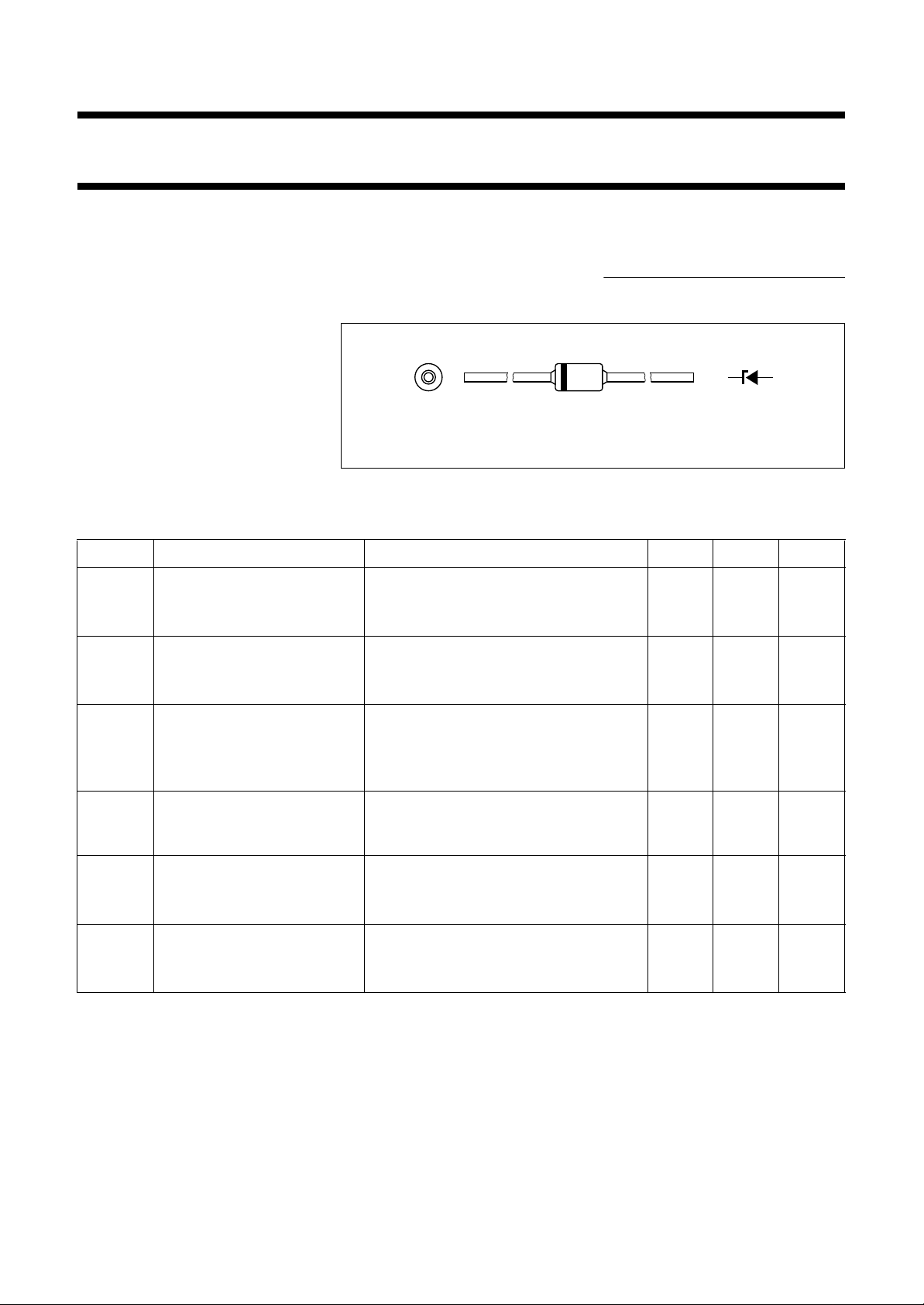
Fig.1 Simplified outline (SOD81) and symbol.
handbook, 4 columns
ak
MAM248
LIMITING VALUES
In accordance with the Absolute Maximum Rating System (IEC 134).
SYMBOL PARAMETER CONDITIONS MIN. MAX. UNIT
P
tot
total power dissipation T
tp
=25°C; lead length 10 mm;
see Figs 2 and 3
BZD23-C3V6 to -C6V8 − 2.0 W
BZD23-C7V5 to -C510 − 2.5 W
P
tot
total power dissipation T
amb
=55°C; see Figs 2 and 3;
PCB mounted (see Fig.7)
BZD23-C3V6 to -C6V8 − 1.0 W
BZD23-C7V5 to -C510 − 1.0 W
P
ZSM
non-repetitive peak reverse
power dissipation
t
p
= 100 µs; square pulse;
T
j
=25°C prior to surge; see Figs 4 and 5
BZD23-C3V6 to -C6V8 − 300 W
BZD23-C7V5 to -C510 − 300 W
P
RSM
non-repetitive peak reverse
power dissipation
10/1000 µs exponential pulse (see Fig.8);
T
j
=25°C prior to surge
BZD23-C7V5 to -C510 − 150 W
T
stg
storage temperature
BZD23-C3V6 to -C6V8 −65 +200 °C
BZD23-C7V5 to -C510 −65 +175 °C
T
j
junction temperature
BZD23-C3V6 to -C6V8 −65 +200 °C
BZD23-C7V5 to -C510 −65 +175 °C
1996 Jun 10 3
Philips Semiconductors Product specification
Voltage regulator diodes BZD23 series
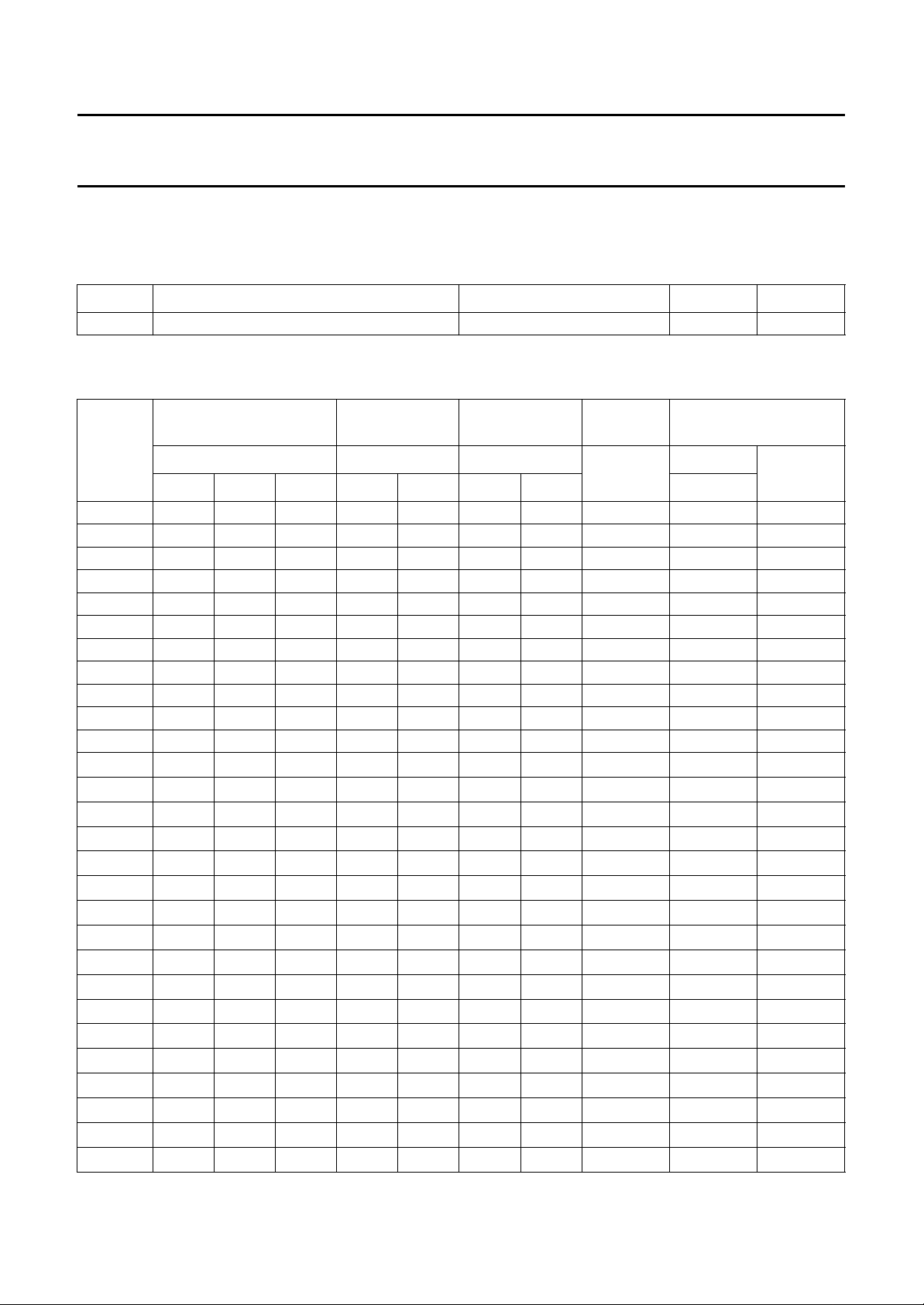
ELECTRICAL CHARACTERISTICS
Total series
T
j
=25°C unless otherwise specified.
Per type when used as voltage regulator diodes
T
j
=25°C unless otherwise specified.
SYMBOL PARAMETER CONDITIONS MAX. UNIT
V
F
forward voltage I
F
= 0.2 A; see Fig.6 1.2 V
TYPE
No.
SUFFIX
(1)
WORKING VOLTAGE
DIFFERENTIAL
RESISTANCE
TEMPERATURE
COEFFICIENT
TEST
CURRENT
REVERSE CURRENT
at REVERSE VOLTAGE
V
Z
(V) at I
Z
r
dif
(Ω)atI
Z
S
Z
(%/K) at I
Z
I
Z
(mA)
I
R
(µA)
V
R
(V)
MIN. NOM. MAX. TYP. MAX. MIN. MAX. MAX.
C3V6 3.4 3.6 3.8 4 8 −0.14 −0.04 100 100 1
C3V9 3.7 3.9 4.1 4 8 −0.14 −0.04 100 50 1
C4V3 4.0 4.3 4.6 4 7 −0.12 −0.02 100 25 1
C4V7 4.4 4.7 5.0 3 7 −0.10 0.00 100 10 1
C5V1 4.8 5.1 5.4 3 6 −0.08 −0.02 100 5 1
C5V6 5.2 5.6 6.0 2 4 −0.04 0.04 100 10 2
C6V2 5.8 6.2 6.6 2 3 −0.01 0.06 100 5 2
C6V8 6.4 6.8 7.2 1 3 0.00 0.07 100 10 3
C7V5 7.0 7.5 7.9 1 2 0.00 0.07 100 50 3
C8V2 7.7 8.2 8.7 1 2 0.03 0.08 100 10 3
C9V1 8.5 9.1 9.6 2 4 0.03 0.08 50 10 5
C10
9.4 10 10.6 2 4 0.05 0.09 50 7 7.5
C11
10.4 11 11.6 4 7 0.05 0.10 50 4 8.2
C12
11.4 12 12.7 4 7 0.05 0.10 50 3 9.1
C13
12.4 13 14.1 5 10 0.05 0.10 50 2 10
C15
13.8 15 15.6 5 10 0.05 0.10 50 1 11
C16
15.3 16 17.1 6 15 0.06 0.11 25 1 12
C18
16.8 18 19.1 6 15 0.06 0.11 25 1 13
C20
18.8 20 21.2 6 15 0.06 0.11 25 1 15
C22
20.8 22 23.3 6 15 0.06 0.11 25 1 16
C24
22.8 24 25.6 7 15 0.06 0.11 25 1 18
C27
25.1 27 28.9 7 15 0.06 0.11 25 1 20
C30
28 30 32 8 15 0.06 0.11 25 1 22
C33
31 33 35 8 15 0.06 0.11 25 1 24
C36
34 36 38 21 40 0.06 0.11 10 1 27
C39
37 39 41 21 40 0.06 0.11 10 1 30
C43
40 43 46 24 45 0.07 0.12 10 1 33
C47
44 47 50 24 45 0.07 0.12 10 1 36
 Loading...