


 Loading...
ORDER NO. KMF0609044CE
Compact Plain Paper Fax (with Digital Answering System)
KX-FP207FX-S
KX-FP218FX-S
(for Eastern Europe)
© 2006 Panasonic Communications Co., Ltd.
All rights reserved. Unauthorized copying and distribution is a violation of law.

KX-FP207FX-S/FP218FX-S |
|
|
TABLE OF CONTENTS |
|
|
|
|
PAGE |
1 |
Safety Precaution ------------------------------------------------- |
3 |
|
1.1. For Service Technicians ---------------------------------- |
3 |
|
1.2. AC Caution--------------------------------------------------- |
3 |
|
1.3. Personal Safety Precautions ---------------------------- |
4 |
|
1.4. Service Precautions --------------------------------------- |
5 |
2 |
Warning -------------------------------------------------------------- |
6 |
|
2.1. About Lead Free Solder (PbF: Pb free) -------------- |
6 |
|
2.2. Insulation Resistance Test ------------------------------- |
7 |
|
2.3. Battery Caution --------------------------------------------- |
7 |
|
2.4. Disposal Cautions------------------------------------------ |
7 |
3 |
Specifications ------------------------------------------------------ |
8 |
4 |
General/Introduction--------------------------------------------- |
9 |
|
4.1. Optional Accessories-------------------------------------- |
9 |
5 |
Features -------------------------------------------------------------- |
9 |
6 |
Technical Descriptions---------------------------------------- |
10 |
|
6.1. Connection Diagram------------------------------------- |
10 |
|
6.2. General Block Diagram--------------------------------- |
11 |
|
6.3. Control Section ------------------------------------------- |
13 |
|
6.4. Facsimile Section ---------------------------------------- |
22 |
|
6.5. Sensors and Switches ---------------------------------- |
29 |
|
6.6. Modem Section ------------------------------------------- |
33 |
|
6.7. NCU Section----------------------------------------------- |
40 |
|
6.8. ITS (Integrated telephone System) |
and |
|
Monitor Section ------------------------------------------- |
43 |
|
6.9. Operation Board Section ------------------------------- |
45 |
|
6.10. LCD Section ----------------------------------------------- |
46 |
|
6.11. Power Supply Board Section-------------------------- |
47 |
7 |
Location of Controls and Components------------------ |
50 |
|
7.1. Overview --------------------------------------------------- |
50 |
|
7.2. Control Panel---------------------------------------------- |
50 |
8 |
Installation Instructions--------------------------------------- |
51 |
|
8.1. Installation Space ---------------------------------------- |
51 |
|
8.2. Connections ----------------------------------------------- |
52 |
|
8.3. Installing the Ink Film------------------------------------ |
53 |
|
8.4. Installing the Paper Tray ------------------------------- |
54 |
|
8.5. Paper Support--------------------------------------------- |
55 |
|
8.6. Installing the Recording Paper------------------------ |
55 |
9 |
Operation Instructions ---------------------------------------- |
56 |
|
9.1. Setting Your Logo ---------------------------------------- |
56 |
10 |
Test Mode---------------------------------------------------------- |
58 |
|
10.1. DTMF Signal Tone Transmit Selection ------------- |
59 |
|
10.2. Button Code Table --------------------------------------- |
60 |
|
10.3. Print Test Pattern----------------------------------------- |
61 |
11 |
Service Mode ----------------------------------------------------- |
62 |
|
11.1. Programing and Lists------------------------------------ |
62 |
|
11.2. The Example of the Printed List ---------------------- |
67 |
12 |
Troubleshooting Guide---------------------------------------- |
72 |
|
12.1. Troubleshooting Summary----------------------------- |
72 |
|
12.2. Error Messages-Display-------------------------------- |
73 |
|
12.3. Error Messages-Report--------------------------------- |
75 |
|
12.4. Remote Programming----------------------------------- |
97 |
|
12.5. Troubleshooting Details ------------------------------ |
100 |
13 |
Service Fixture & Tools ------------------------------------- |
136 |
14 |
Disassembly and Assembly Instructions------------- |
137 |
|
14.1. General Section ---------------------------------------- |
137 |
|
14.2. Disassembly Flowchart ------------------------------- |
138 |
|
14.3. Disassembly Procedure ------------------------------ |
140 |
15 |
Maintenace ------------------------------------------------------ |
163 |
PAGE |
|
15.1. Maintenance Items and Component Locations -163 |
|
15.2. Gear Section--------------------------------------------- |
165 |
15.3. Jams ------------------------------------------------------- |
172 |
15.4. Cleaning--------------------------------------------------- |
174 |
16 Miscellaneous -------------------------------------------------- |
176 |
16.1. Terminal Guide of the ICs Transistors and |
|
Diodes ----------------------------------------------------- |
176 |
16.2. How to Replace the Flat Package IC -------------- |
178 |
16.3. Test Chart------------------------------------------------- |
180 |
17 Schematic Diagram ------------------------------------------- |
183 |
17.1. Digital Board (PCB1) (KX-FP207FX) -------------- |
183 |
17.2. Digital Board (PCB1) (KX-FP218FX) -------------- |
187 |
17.3. Analog Board (PCB2) (KX-FP207FX) ------------ |
191 |
17.4. Analog board (PCB2) (KX-FP218FX) ------------- |
193 |
17.5. Operation Board (PCB3) (KX-FP207FX) --------- |
195 |
17.6. Operation Board (PCB3) (KX-FP218FX) --------- |
196 |
17.7. Power Supply Board (PCB4) ------------------------ |
197 |
17.8. Interface Board (PCB5) ------------------------------- |
198 |
17.9. Sensor Board (PCB6) --------------------------------- |
199 |
17.10. Film End SensorBoard (PCB7)--------------------- |
199 |
17.11. Motor Position Sensor Board (PCB8) ------------- |
199 |
17.12. Hook Switch Board (PCB9) -------------------------- |
200 |
18 Printed Circuit Board----------------------------------------- |
202 |
18.1. Digital Board (PCB1)----------------------------------- |
202 |
18.2. Analog Board (PCB2) --------------------------------- |
204 |
18.3. Operation Board (PCB3)------------------------------ |
206 |
18.4. Power Supply Board (PCB4) ------------------------ |
208 |
18.5. Interface Board (PCB5) ------------------------------- |
209 |
18.6. Sensor Board (PCB6) --------------------------------- |
209 |
18.7. Film End Sensor Board (PCB7)--------------------- |
209 |
18.8. Motor Position Sensor Board (PCB8) ------------- |
209 |
18.9. Hook Switch Board (PCB9) -------------------------- |
210 |
19 Appendix Information of Schematic Diagram ------- |
210 |
20 Exploded View and Replacement Parts List---------- |
211 |
20.1. Cabinet, Mechanical and Electrical Parts |
|
Location --------------------------------------------------- |
211 |
20.2. Replacement Parts List ------------------------------- |
221 |
2

KX-FP207FX-S/FP218FX-S
1Safety Precaution
1.Before servicing, unplug the AC power cord to prevent an electric shock.
2.When replacing parts, use only the manufacturer's recommended components.
3.Check the condition of the power cord. Replace if wear or damage is evident.
4.After servicing, be sure to restore the lead dress, insulation barriers, insulation papers, shields, etc.
5.Before returning the serviced equipment to the customer, be sure to perform the following insulation resistance test to prevent the customer from being exposed to shock hazards.
1.1.For Service Technicians
ICs and LSIs are vulnerable to static electricity.
When repairing, the following precautions will help prevent recurring malfunctions.
1.Cover the plastic part's boxes with aluminum foil.
2.Ground the soldering irons.
3.Use a conductive mat on the worktable.
4.Do not touch the IC or LSI pins with bare fingers.
1.2.AC Caution
For safety, before closing the lower cabinet, please make sure of the following precautions.
1.The earth lead is fixed with the screw.
2.The AC lead is connected properly to power supply board.
3.Wrap the earth lead around the core 5 times.
4.Wrap the AC lead around the core 5 times.
3
KX-FP207FX-S/FP218FX-S
1.3.Personal Safety Precautions
1.3.1.Moving Sections of the Unit
Be careful not to let your hair, clothes, fingers, accessories, etc., become caught in any moving sections of the unit.
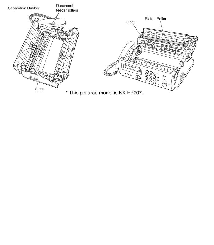
The moving sections of the unit are the rollers and a gear. There is a separation roller and a document feed roller which are rotated by the document feed motor. A gear rotates the two rollers. Be careful not to touch them with your hands, especially when the unit is operating.
1.3.2.Live Electrical Sections
All the electrical sections of the unit supplied with AC power by the AC power cord are live.
Never disassemble the unit for service with the AC power supply plugged in.
CAUTION:
AC voltage is supplied to the primary side of the power supply unit. Therefore, always unplug the AC power cord before disassembling for service.
4
KX-FP207FX-S/FP218FX-S
1.4.Service Precautions
1.4.1.Precautions to Prevent Damage from static Electricity
Electrical charges accumulate on a person. For instance, clothes rubbing together can damage electric elements or change their electrical characteristics. In order to prevent static electricity, touch a metallic part that is grounded to release the static electricity. Never touch the electrical sections such as the power supply unit, etc.
5
KX-FP207FX-S/FP218FX-S
2 Warning
2.1.About Lead Free Solder (PbF: Pb free)
Note:
In the information below, Pb, the symbol for lead in the periodic table of elements, will refer to standard solder or solder that contains lead.
We will use PbF solder when discussing the lead free solder used in our manufacturing process which is made from Tin, (Sn), Silver, (Ag), and Copper, (Cu).
This model, and others like it, manufactured using lead free solder will have PbF stamped on the PCB. For service and repair work we suggest using the same type of solder.
Caution
•PbF solder has a melting point that is 50° ~ 70° F, (30° ~ 40°C) higher than Pb solder. Please use a soldering iron with temperature control and adjust it to 700° ± 20° F, (370° ± 10°C).
•Exercise care while using higher temperature soldering irons.: Do not heat the PCB for too long time in order to prevent solder splash or damage to the PCB.
•PbF solder will tend to splash if it is heated much higher than its melting point, approximately 1100°F, (600°C).
•When applying PbF solder to double layered boards, please check the component side for excess which may flow onto the opposite side (See figure, below).
2.1.1.Suggested PbF Solder
There are several types of PbF solder available commercially. While this product is manufactured using Tin, Silver, and Copper, (Sn+Ag+Cu), you can also use Tin and Copper, (Sn+Cu), or Tin, Zinc, and Bismuth, (Sn+Zn+Bi). Please check the manufacturer’s specific instructions for the melting points of their products and any precautions for using their product with other materials.
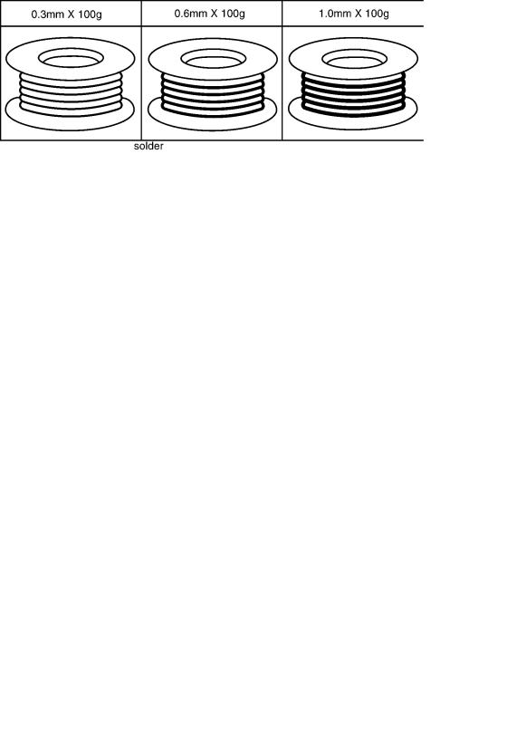
The following lead free (PbF) solder wire sizes are recommended for service of this product: 0.3mm, 0.6mm and 1.0mm.
6

KX-FP207FX-S/FP218FX-S
2.2.Insulation Resistance Test
1.Unplug the power cord and short the two prongs of the plug with a jumper wire.
2.Turn on the power switch.
3.Measure the resistance value with an ohmmeter between the jumpered AC plug and each exposed metal cabinet part (screw heads, control shafts, bottom frame, etc.).
Note: Some exposed parts may be isolated from the chassis by design. These will read infinity.
4.If the measurement is outside the specified limits, there is a possibility of a shock hazard.
2.3.Battery Caution
Danger of explosion if battery is incorrectly replaced. Replace only with the same or equivalent type recommended by the manufacturer. Dispose of used batteries according to the manufacturer’s instruction.
CAUTION:
The lithium battery is a critical component (type No. CR2032). Please observe for the proper polarity and the exact location when replacing it and soldering the replacement lithium battery in.
2.4.Disposal Cautions
2.4.1.Information on Disposal for Users of Waste Electrical & Electronic Equipment (private households)
This symbol on the products and/or accompanying documents means that used electrical and electronic products should not be mixed with general household waste.
For proper treatment, recovery and recycling, please take these products to designated collection points, where they will be accepted on a free of charge basis. Alternatively, in some countries you may be able to return your products to your local retailer upon the purchase of an equivalent new product.
Disposing of this product correctly will help to save valuable resources and prevent any potential negative effects on human health and the environment which could otherwise arise from inappropriate waste handling. Please contact your local authority for further details of your nearest designated collection point.Penalties may be applicable for incorrect disposal of this waste, in accordance with national legislation.
For business users in the European Union
If you wish to discard electrical and electronic equipment, please contact your dealer or supplier for further information.
Information on Disposal in other Countries outside the European Union
This symbol is only valid in the European Union.
If you wish to discard this product, please contact your local authorities or dealer and ask for the correct method of disposal.
7

KX-FP207FX-S/FP218FX-S
3 Specifications
Any details given in these instructions are subject to change without notice.
Applicable Lines: |
Public Switched Telephone Network |
|
Document Size: |
Max. 216 mm in width, Max. 600 mm in length |
|
Effective Scanning Width: |
208 mm |
|
Recording Paper Size: |
A4: 210 mm × 297 mm |
|
Effective Printing Width: |
A4: 202 mm |
|
Recording Paper Weight: |
64 g/m2 to 80 g/m2 |
|
Transmission Speed*1 (KX-FP207): |
Approx. |
12 s/page (ECM-MMR)*2 |
Transmission Speed*1 (KX-FP218): |
Approx. |
8 s/page (ECM-MMR)*2 |
Scanning Density: |
Horizontal: 8 pels/mm |
|
|
Vertical: |
|
|
3.85 lines/mm (standard resolution) |
|
|
7.7 lines/mm (fine/photo resolution) |
|
|
15.4 lines/mm (super fine resolution) |
|
Photo Resolution: |
64 levels |
|
Scanner Type: |
Contact Image Sensor |
|
Printer Type: |
Thermal Transfer on Plain Paper |
|
Data Compression System: |
Modified Huffman (MH), Modified READ (MR), Modified Modified READ (MMR) |
|
Modem Speed (KX-FP207): |
9,600 / 7,200 / 4,800 / 2,400 bps; Automatic Fallback |
|
Modem Speed (KX-FP218): |
14,400 / 12,000 / 9,600 / 7,200 / 4,800 / 2,400 bps; Automatic Fallback |
|
Operating Environment: |
5—35°C, 20—80 % RH (Relative Humidity) |
|
Dimensions: |
Approx. height 106 mm × width 356 mm × depth 200 mm |
|
Mass (Weight): |
Approx. 2.7 kg |
|
Power Consumption: |
Standby: Approx. 1.5 W |
|
|
Transmission: Approx. 15 W |
|
|
Reception: Approx. 40 W (When receiving a 20% black document) |
|
|
Copy: Approx. 40 W (When copying a 20% black document) |
|
|
Maximum: Approx. 135 W (When copying a 100% black document) |
|
Power Supply: |
220 - 240 V AC, 50 / 60 Hz |
|
Fax Memory Capacity*3: |
Transmission: Approx. 25 pages |
|
|
Reception: Approx. 28 pages |
|
|
(Based on the ITU-T No. 1 Test Chart in standard resolution, without using the Error |
|
|
Correction Mode.) |
|
Voice Memory Capacity*4 |
Approx. 18 minutes of recording time including greeting messages |
|
(KX-FP218): |
|
|
*1 Transmission speed depends on the contents of the pages, resolution, telephone line conditions and capability of the other party’s machine.
*2 Transmission speed is based on the ITU-T No. 1 Test Chart with original mode. If the capability of the other party’s machine is inferior to your unit, the transmission time may be longer. (Refer to ITU-T No.1 Test chart (P.180).)
*3 If an error occurs during fax reception, such as a paper jam or if the recording paper runs out, the fax and subsequent faxes will be retained in memory.
*4 Recording time may be reduced by the calling party’s background noise.
8

KX-FP207FX-S/FP218FX-S
4 General/Introduction
4.1.Optional Accessories
Model No. |
Description |
Specification |
|
|
|
KX-FA52E |
Replacement Film*1 |
30 m × 2 rolls |
|
|
(Each roll will print about 90 A4-sized pages) |
*1 To ensure the unit operates properly, we recommend using the Panasonic replacement film.
The ink film is not reusable. Do not rewind and use the ink film again.
5 Features
General
• LCD (Liquid Crystal Display) readout
Plain Paper Facsimile Machine
•12 second transmission speed (KX-FP207)*
•8 second transmission speed (KX-FP218)**
•A4, G3 compatible
•Automatic document feeder (up to 10 sheets)
•Quick scan
•Resolution: Standard/Fine/Super fine/Photo (64 level)
•Broadcast
•20-sheet recording paper capacity
•Automatic fax/phone switching
*The 12 second speed is based upon the ITU-T No. 1 Test Chart on the condition that memory transmission is performed.
**The 8 second speed is based upon the ITU-T No. 1 Test Chart on the condition that memory transmission is performed.
Large Memory... Performed by DRAM
Approx. 28 pages of memory reception
Approx. 25 pages of memory transmission
Integrated Telephone System
•On-hook dialling
•Voice muting
•Redialling function
•50-station telephone directory with Phonebook
•Caller ID service
This unit is compatible with the Caller ID service offered by your local telephone company. To use this unit’s Caller ID features, you must subscribe to Caller ID service.
Important:
-This unit is designed in accordance with the ETS (European Telecommunication Standard) and only supports the basic CLIP (Calling Line Identification Presentation) features.
-This unit will only display the caller’s telephone number and name.
-This unit will not support future additional telephone services.
-Depending on the service of the local telephone company, the date/time of the call or the caller’s name may
not be displayed.
Make sure the following ring count is set to 2 or more rings beforehand.
-For KX-FP207: FAX ring count (feature #06 on P.98) and TEL/FAX ring count (feature #78 on P.98)
-For KX-FP218: TAM ring count (feature #06 on P.98) FAX ring count (feature #06 on P.98) and TEL/FAX ring count (feature #78 on P.98)
•SP-Phone, TAM (KX-FP218)
Enhanced Copier Function
•Multi-copy function (up to 20 copies)
•Enlargement and reduction
•Collate
•64-Level halftone
9
KX-FP207FX-S/FP218FX-S
6 Technical Descriptions
6.1.Connection Diagram
10
KX-FP207FX-S/FP218FX-S
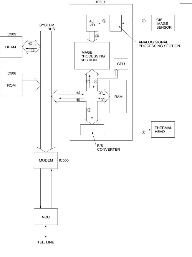
6.2.General Block Diagram
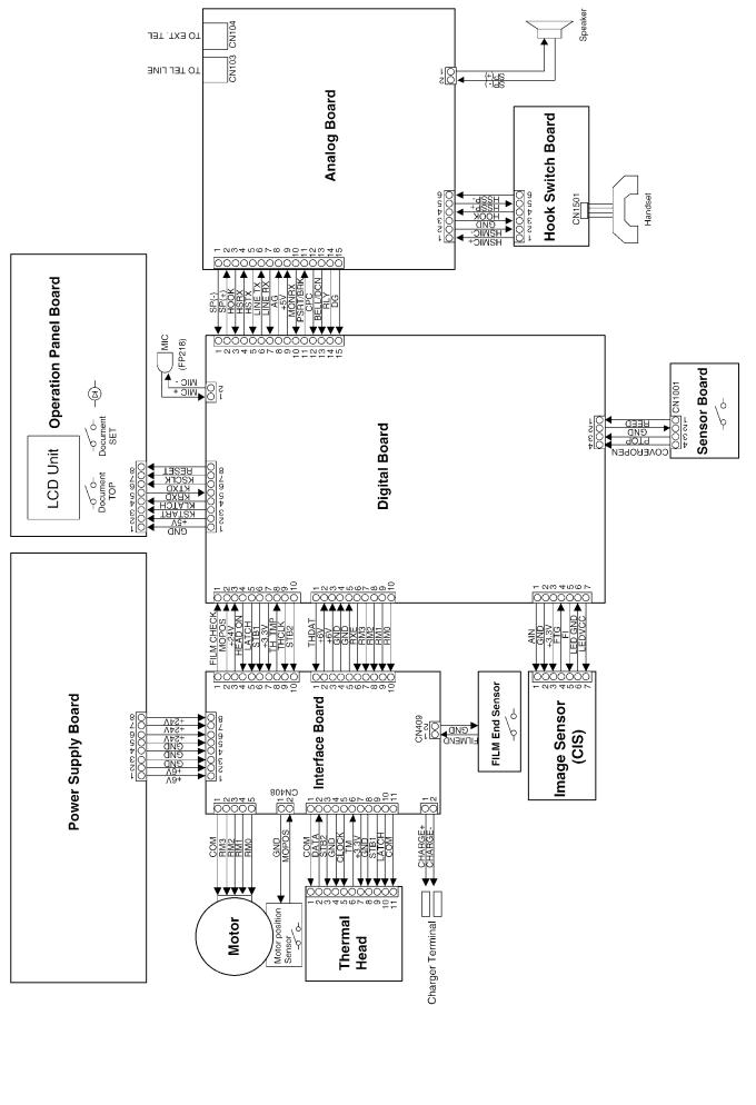
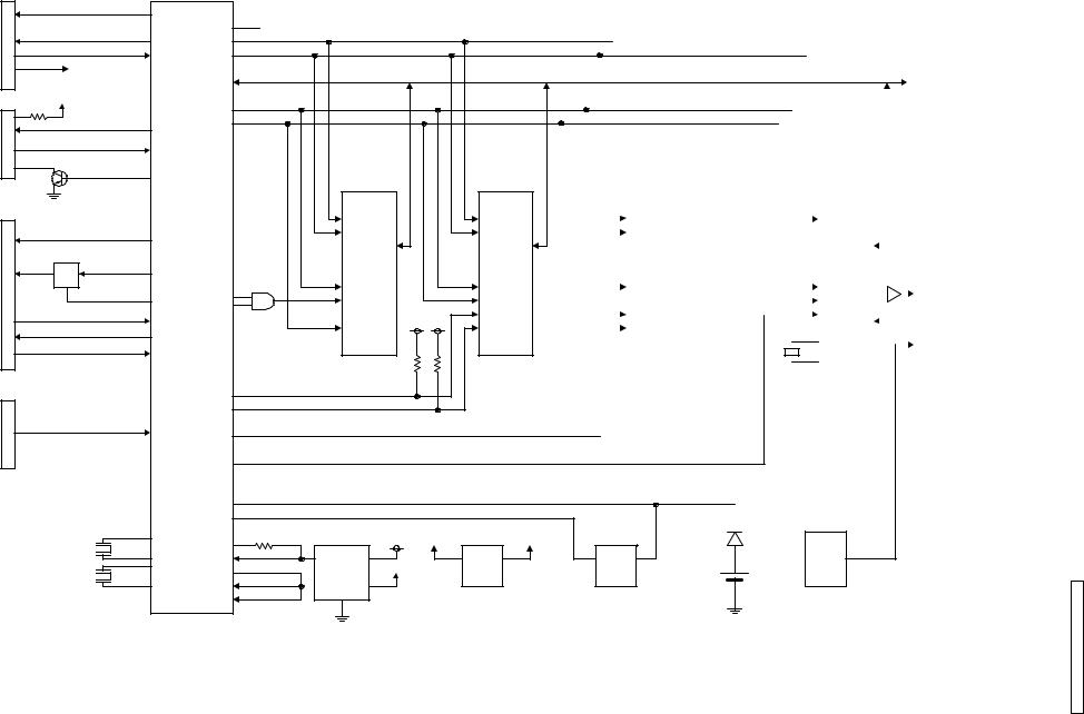
The following is an outline of each device IC on the digital board. (Refer to General Block Diagram (P.12).).
1.ASIC (IC501)
Composed mainly of an address decoder and a modem control. Controls the general FAX operations.
Controls the operation panel I/F.
Controls the thermal head I/F and CIS I/F. Performs the image processing.
CPU and Real time clock
Provides the reset pulse for each of the major ICs.
2.Flash ROM (IC506)
Contains all of the program instructions on the unit operations.
This memory is used mainly for the parameter working in the storage area.
3.Dynamic RAM (IC503)
This memory is used mainly for the parameter working in the storage area.
4.MODEM (IC505)
Performs the modulation and the demodulation for FAX communication.
5.Read Section
CIS image sensor to read transmitted documents.
6.Motor Driver (IC401)
Drives the transmission motor and the reception motor.
7.Thermal Head
Contains heat-emitting elements for dot matrix image printing.
8.Analogue Board
Composed of ITS circuit and NCU circuit.
9.Sensor Section
Composed of a cover open and film end switch, a document set switch, a document top switch, a paper top sensor and a motor position switch.
10.Power Supply Board Switching Section Supplies +6V and +24V to the unit.
11.Flash Memory (IC507) (KX-FP218 Only)
This memory is used for voice prompt and TAM.
11

KX-FP207FX-S/FP218FX-S
6.2.1.General Block Diagram
12
|
|
|
IC501 |
|
CN501 |
|
ASIC |
||
|
|
OP-RESET |
|
|
|
KSTART,KLATCH |
ADR[15:13] |
||
|
KSCLK,KTXD |
RBA[5:0] |
||
ration |
KRXD |
|||
ADR[12:0] |
||||
el |
MIC IN |
|||
|
||||
|
|
|
||
|
|
|
DB[7:0] |
|
CN505 |
+5V |
|
||
|
XRD |
|||
|
|
|
||
TO |
|
F1,FTG |
XWR |
|
|
|
|
||
CIS |
VIDEO |
|
||
|
|
CISLEDON |
A[12:0] |
|
|
|
|
||
CN502,503 |
|
|||
|
|
THLAT,THC,THDAT |
|
|
|
|
STB1,STB2 |
|
|
|
|
Q501,502,504 |
IC509 |
|
|
|
HEADON |
||
|
|
|
AND |
|
|
|
RXE |
XROMCS |
|
|
|
TM |
XOPRBE |
|
13 |
|
|
||
|
RXE,RM0~3 |
|
||
|
|
FILM_CHECK,MOTOR_POS |
|
|
CN504 |
|
XRAS |
||
|
|
|
||
|
|
|
XCAS |
|
|
|
REED,PTOP,COVER OPEN |
XRESCS2 |
|
|
|
|
||
|
|
|
XMDMCS |
|
|
|
|
+3.3V/BATT |
|
|
|
|
+2.5V/BATT |
|
|
|
24MHz |
XWDERR |
|
|
|
XRESETI |
||
|
|
|
||
|
|
32.768KHz |
XORESET |
|
|
|
XRESET |
||
|
|
|
||
|
|
|
XBACKEN |
|
RBA[5:0] |
IC506 |
A[7:4] |
RBA[5:0] |
IC503 |
|
FLASH |
DRAM |
||||
|
|
|
|||
|
A[17:0] |
|
|
A[9:0] |
|
|
D[7:0] |
|
|
D[7:0] |
|
|
XRD |
|
|
XRD |
|
|
XCS |
|
|
XWR |
|
|
|
+3.3V |
|
XRAS |
|
|
XWR |
|
XCAS |
||
|
|
|
+2.5V/BATT
IC504
RESET-IC +5V +2.5V Q503 +3.3V
VDET IN
+3.3V
OUT
GND
|
A[12:0] |
|
RBA[5:0] |
|
|
IC507 |
|
|
|
|
|
||||
|
|
|
|
||||
|
|
|
|
||||
|
|
|
|
FLASH |
|||
|
|
|
|
|
|
||
|
|
|
|
|
|
A[17:0] |
|
|
|
|
|
|
|
|
|
|
|
|
|
|
|
D[7:0] |
|
|
|
|
|
|
|
XRD |
|
|
|
|
|
|
|
|
|
|
|
|
|
|
|
XCS |
|
|
|
|
|
|
|
|
|
|
|
|
|
|
|
XWR |
|
|
|
|
|
|
|
|
|
|
|
|
|
|
|
|
|
|
|
|
|
|
(KX-FP218) |
||
|
|
|
|
|
|
|
|
+3.3V/BATT
Q505
+
-
|
|
|
A[4:0] |
|
|
IC505 |
|
|
|
|
|
|
|
|
|
|
|
|
|
|
|
|
|
|
|
|
|
|
|||
|
|
|
|
|
|
|
|
|
|
|
|
|
|||
|
|
|
|
|
|
|
|
|
|
|
|
|
|||
|
|
|
|
MODEM |
|
|
|
|
|
|
|
|
|||
|
|
|
|
|
|
|
|
|
|
|
|
|
|
|
|
|
|
|
|
|
|
|
A[4:0] |
|
|
|
|
|
|
|
|
|
|
|
|
|
|
|
|
|
|
|
|
|
|
|
|
|
|
|
|
|
|
|
D[7:0] |
|
|
|
|
CN507 |
|||
|
|
|
|
|
|
|
|
|
|
|
|||||
|
|
|
|
|
|
|
|
|
|
|
|
||||
|
|
|
|
|
|
|
XRD |
|
|
|
|
|
|
|
TO |
|
|
|
|
|
|
|
|
|
|
|
|
|
|
||
|
|
|
|
|
|
|
TX |
|
|
|
|
|
|
|
Analog |
|
|
|
|
|
|
|
|
|
|
|
|
|
|
||
|
|
|
|
|
|
|
XWR |
|
|
|
|
|
|
|
|
|
|
|
|
|
|
|
|
|
|
|
|
|
|
||
|
|
|
|
|
|
|
XCS |
|
|
|
|
|
|
|
Board |
|
|
|
|
|
|
|
|
|
|
|
|
|
|
||
|
|
|
|
|
|
|
RX |
|
|
|
|
|
|
|
|
|
|
|
|
|
|
|
|
|
|
|
|
|
|
|
|
|
|
|
|
|
|
|
|
|
|
|
|||||
|
|
|
|
|
|
|
|
|
|
|
|
|
|
|
|
|
|
|
|
|
|
|
|
|
|
|
|
||||
|
|
|
|
|
|
|
|
|
|
|
|
||||
32.256MHz |
|
|
|
|
|
|
|
|
|
||||||
|
|
|
|
|
|
|
|
|
|||||||
|
|
|
|
|
|
|
|
|
|
|
|
|
|
|
|
IC510
SP-AMP
BATT
KX-FP207/218FX-S : CONTROL SECTION BLOCK DIAGRA M
1.3.6 |
.3.6 |
. |
|
Diagram Block |
Section Control |
S-S/FP218FX-FP207FX-KX
KX-FP207FX-S/FP218FX-S
6.3.2.Memory Map
14
KX-FP207FX-S/FP218FX-S
6.3.3.ASIC (IC501)
This custom IC is used for the general FAX operations.
1.CPU:
This model uses a Z80 equivalent to the CPU operating at 12 MHz. Most of the peripheral functions are performed by custom-designed LSIs. Therefore, the CPU only works for processing the results.
2.RTC:
Real Time Clock
3.DECODER: Decodes the address.
4.ROM/RAM I/F:
Controls the SELECT signal of ROM or RAM and the bank switching.
5.CIS I/F:
Controls the document reading.
6.IMAGE DATA RAM:
This memory is programmed into the ASIC and uses 8 KB for the image processing. (See Fig. A.*)
7.THERMAL HEAD I/F:
Transmits the recorded data to the thermal head.
8.MOTOR I/F:
Controls the transmission motor which feeds the document.
Controls the receiving motor which feeds the recording paper.
9.OPERATION PANEL I/F:
Serial interface with Operation Panel.
10.I/O PORT:
I/O Port Interface.
11.ANALOGUE UNIT:
Electronic volume for the monitor. Sends beep tones, etc.
Fig. A
Note:
This memory is incorporated into the ASIC (IC501) and used for the image processing. Fig. A shows the memory map of the Image Data RAM.
15

KX-FP207FX-S/FP218FX-S
Descriptions of Pin Distribution (IC501)
NO. |
SIGNAL |
I/O |
POWER SUPPLIED |
DESCRIPTION |
|
|
|
VOLTAGE |
|
|
|
|
|
|
1 |
VSSA |
|
GND |
POWER SOURCE (ANALOG GND) |
|
|
|
|
|
2 |
VDDA 3.3 |
|
3.3V |
POWER SOURCE (ANALOG +3.3V) |
3 |
AIN1 |
A |
3.3V |
CIS IMAGE SIGNAL INPUT (SIG) |
|
|
|
|
|
4 |
AIN2 |
A |
3.3V |
THERMISTOR TEMPERATURE WATCH INPUT |
5 |
AIN3 |
A |
3.3V |
LINE VOLTAGE DETECTION SIGNAL INPUT (DCIN) |
|
|
|
|
|
6 |
AMON |
A |
3.3V |
ANALOG SIGNAL MONITOR TERMINAL |
7 |
VSS |
|
GND |
POWER SOURCE (GND) |
|
|
|
|
|
8 |
X32OUT |
O |
3.3V/BATT |
RTC (32.768KHz) CONNECTION |
9 |
X32IN |
I |
3.3V/BATT |
RTC (32.768KHz) CONNECTION |
|
|
|
|
|
10 |
VDD (3.3V / B) |
|
----- |
POWER SOURCE (+3.3V/LITHIUM BATTERY) |
11 |
XBACEN |
I |
3.3V/BATT |
BACKUP ENABLE |
|
|
|
|
|
12 |
XRAMCS |
O |
3.3V/BATT |
NOT USED |
13 |
VDD (3.3V / B) |
|
----- |
POWER SOURCE(+3.3V / LITHIUM BATTERY) |
|
|
|
|
|
14 |
VDD (2.5V/B) |
|
----- |
POWER SOURCE (+2.5V / LITHIUM BATTERY) |
15 |
FTG |
O |
3.3V |
SH SIGNAL OUTPUT FOR CIS (SI) |
|
|
|
|
|
16 |
F1 |
O |
3.3V |
01 SIGNAL OUTPUT FOR CIS (CLK) |
|
|
|
|
|
17 |
F2/OP |
O |
3.3V |
OUTPUT PORT (THON) |
18 |
FR/OP |
O |
3.3V |
OUTPUT PORT (MDMRST) |
|
|
|
|
|
19 |
CPC |
I |
3.3V |
INPUT PORT (CPC) |
20 |
RVN |
I |
3.3V |
INPUT PORT (REED) |
|
|
|
|
|
21 |
IRDATXD/IOP |
O |
3.3V |
OUTPUT PORT (CISLED) |
22 |
IRDARXD/IOP80 |
I |
3.3V |
INPUT PORT (PTOP) |
|
|
|
|
|
23 |
TXD/IOP |
I |
3.3V |
INPUT PORT (FILMEND) |
24 |
RXD/IOP |
O |
3.3V |
OUTPUT PORT (HS-ALC) |
|
|
|
|
|
25 |
XRTS/IOP |
I |
3.3V |
INPUT PORT (HOOK) |
26 |
XCTS/IOP |
O |
3.3V |
OUTPUT PORT (SPMUTE) |
|
|
|
|
|
27 |
VDD (2.5V) |
|
----- |
POWER SOURCE (+2.5V) |
28 |
TONE1 |
A |
3.3V |
TONE OUTPUT |
|
|
|
|
|
29 |
TONE2 |
A |
3.3V |
TONE OUTPUT |
|
|
|
|
|
30 |
VOLUREF |
A |
3.3V |
ANALOG REF VOLTAGE |
|
|
|
|
|
31 |
VOLUOUT |
A |
3.3V |
VOLUME OUTPUT |
|
|
|
|
|
32 |
VOLUIN |
A |
3.3V |
VOLUME INPUT |
33 |
XNMI |
I |
3.3V |
HIGH FIXED |
|
|
|
|
|
34 |
FMEMDO/IOP |
O |
3.3V |
OUTPUT PORT (CIS ON) |
35 |
VDD (3.3V) |
|
----- |
POWER SOURCE (+3.3V) |
|
|
|
|
|
36 |
VSS |
|
GND |
POWER SOURCE (GND) |
37 |
VSS |
|
GND |
POWER SOURCE (GND) |
|
|
|
|
|
38 |
VDD (3.3V) |
|
----- |
POWER SOURCE (+3.3V) |
39 |
MIDAT/IOP |
O |
3.3V |
PORT (DATA) |
|
|
|
|
|
40 |
MICLK/IOP |
O |
3.3V |
PORT (DR) |
41 |
MILAT/IOP |
O |
3.3V |
PORT (CD) |
|
|
|
|
|
42 |
20KOSC/IOP |
I/O |
3.3V |
PORT (TONEIEN) |
43 |
XWAIT |
I |
3.3V |
INPUT PORT (MPOS) |
|
|
|
|
|
44 |
HSTRD/IOP |
O |
3.3V |
OUTPUT (DCLK) |
|
|
|
|
|
45 |
HSTWR/IOP |
O |
3.3V |
OUTPUT PORT (XHSTWR) |
|
|
|
|
|
46 |
XOPRBE |
O |
3.3V |
MFCS |
|
|
|
|
|
47 |
ADR15 |
O |
3.3V |
CPU ADDRESS BUS 15 (NOT USED) |
48 |
ADR14 |
O |
3.3V |
CPU ADDRESS BUS 14 (NOT USED) |
|
|
|
|
|
49 |
ADR13 |
O |
3.3V |
CPU ADDRESS BUS 13 (NOT USED) |
50 |
VDD (2.5V) |
|
----- |
POWER SOURCE (+2.5V) |
|
|
|
|
|
51 |
XOUT |
O |
3.3V |
SYSTEM CLOCK (24MHz) |
52 |
XIN |
I |
3.3V |
SYSTEM CLOCK (24MHz) |
|
|
|
|
|
53 |
VSS |
|
GND |
POWER SOURCE (GND) |
54 |
VDD (3.3V) |
|
----- |
POWER SOURCE (+3.3V) |
|
|
|
|
|
55 |
XTEST |
O |
3.3V |
24MHz CLOCK |
56 |
TEST1 |
I |
3.3V |
HIGH FIXED |
|
|
|
|
|
16

KX-FP207FX-S/FP218FX-S
NO. |
SIGNAL |
I/O |
POWER SUPPLIED |
DESCRIPTION |
|
|
|
VOLTAGE |
|
|
|
|
|
|
57 |
TEST2 |
I |
3.3V |
HIGH FIXED |
|
|
|
|
|
58 |
TEST3 |
I |
3.3V |
HIGH FIXED |
59 |
TEST4 |
I |
3.3V |
HIGH FIXED |
|
|
|
|
|
60 |
XMDMINT |
I |
3.3V |
MODEM INTERRUPT |
61 |
XMDMCS |
O |
3.3V |
MODEM CHIP SELECT |
|
|
|
|
|
62 |
XRAS/IOP |
O |
3.3V |
DRAM (IC503) ROW ADDRESS STROBE |
63 |
XCAS1/IOP |
O |
3.3V |
DRAM (IC503) CULUM ADDRESS STROBE |
|
|
|
|
|
64 |
XCAS2/IOP |
I |
3.3V |
INPUT PORT (COVER) |
65 |
XRESCS2 |
O |
3.3V |
FLASH CHIP SELECT (XRESCS2) |
|
|
|
|
|
66 |
DB3 |
I/O |
3.3V |
CPU DATA BUS 3 |
67 |
DB2 |
I/O |
3.3V |
CPU DATA BUS 2 |
|
|
|
|
|
68 |
DB4 |
I/O |
3.3V |
CPU DATA BUS 4 |
69 |
DB1 |
I/O |
3.3V |
CPU DATA BUS 1 |
|
|
|
|
|
70 |
DB5 |
I/O |
3.3V |
CPU DATA BUS 5 |
71 |
VDD (3.3V) |
|
----- |
POWER SOURCE (+3.3V) |
|
|
|
|
|
72 |
VSS |
|
GND |
POWER SOURCE (GND) |
|
|
|
|
|
73 |
VSS |
|
GND |
POWER SOURCE (GND) |
74 |
VDD (3.3V) |
|
----- |
POWER SOURCE (+3.3V) |
|
|
|
|
|
75 |
DB0 |
I/O |
3.3V |
CPU DATA BUS 0 |
76 |
DB6 |
I/O |
3.3V |
CPU DATA BUS 6 |
|
|
|
|
|
77 |
DB7 |
I/O |
3.3V |
CPU DATA BUS 7 |
78 |
XROMCS |
O |
3.3V |
ROM (IC502) CHIP SELECT |
|
|
|
|
|
79 |
RD |
O |
3.3V |
CPU RD |
80 |
WR |
O |
3.3V |
CPU WR |
|
|
|
|
|
81 |
ADR0 |
O |
3.3V |
CPU ADDRESS BUS 0 |
82 |
ADR1 |
O |
3.3V |
CPU ADDRESS BUS 1 |
|
|
|
|
|
83 |
ADR2 |
O |
3.3V |
CPU ADDRESS BUS 2 |
84 |
ADR3 |
O |
3.3V |
CPU ADDRESS BUS 3 |
|
|
|
|
|
85 |
ADR4 |
O |
3.3V |
CPU ADDRESS BUS 4 |
|
|
|
|
|
86 |
ADR5 |
O |
3.3V |
CPU ADDRESS BUS 5 |
|
|
|
|
|
87 |
VSS |
|
GND |
POWER SOURCE (GND) |
|
|
|
|
|
88 |
VDD (2.5V) |
|
----- |
POWER SOURCE (+2.5V) |
89 |
ADR6 |
O |
3.3V |
CPU ADDRESS BUS 6 |
|
|
|
|
|
90 |
ADR7 |
O |
3.3V |
CPU ADDRESS BUS 7 |
91 |
ADR8 |
O |
3.3V |
CPU ADDRESS BUS 8 |
|
|
|
|
|
92 |
ADR9 |
O |
3.3V |
CPU ADDRESS 9 |
93 |
ADR10 |
O |
3.3V |
CPU ADDRESS 10 |
|
|
|
|
|
94 |
ADR11 |
O |
3.3V |
CPU ADDRESS 11 |
95 |
ADR12 |
O |
3.3V |
CPU ADDRESS 12 |
|
|
|
|
|
96 |
RBA0 |
O |
3.3V |
ROM/RAM BANK ADDRESS 0 |
97 |
RBA1 |
O |
3.3V |
ROM/RAM BANK ADDRESS 1 |
|
|
|
|
|
98 |
RBA2 |
O |
3.3V |
ROM/RAM BANK ADDRESS 2 |
99 |
RBA3 |
O |
3.3V |
ROM/RAM BANK ADDRESS 3 |
|
|
|
|
|
100 |
RBA4 |
O |
3.3V |
ROM/RAM BANK ADDRESS 4 |
|
|
|
|
|
101 |
RBA5 |
O |
3.3V |
ROM/RAM BANK ADDRESS 5 |
|
|
|
|
|
102 |
RBA6/IOP96 |
O |
3.3V |
A19 |
|
|
|
|
|
103 |
STB1 |
O |
3.3V |
STROBE SIGNAL OUTPUT TO THERMAL HEAD |
104 |
STB2 |
O |
3.3V |
STROBE SIGNAL OUTPUT TO THERMAL HEAD |
|
|
|
|
|
105 |
STB3 |
O |
3.3V |
STROBE SIGNAL OUTPUT TO THERMAL HEAD |
106 |
XRESET |
I |
3.3V |
RESET INPUT |
|
|
|
|
|
107 |
VDD (3.3V) |
|
----- |
POWER SOURCE (+3.3V) |
108 |
VSS |
|
GND |
POWER SOURCE (GND) |
|
|
|
|
|
109 |
VSS |
|
GND |
POWER SOURCE (GND) |
110 |
VDD (3.3V) |
|
----- |
POWER SOURCE (+3.3V) |
|
|
|
|
|
111 |
XORESET |
O |
3.3V |
NOT USED |
112 |
VDD(5V) |
|
----- |
POWER SOURCE (+5V) |
|
|
|
|
|
113 |
VSS |
|
GND |
POWER SOURCE (GND) |
17

KX-FP207FX-S/FP218FX-S
NO. |
SIGNAL |
I/O |
POWER SUPPLIED |
DESCRIPTION |
|
|
|
VOLTAGE |
|
|
|
|
|
|
114 |
XRESETI |
I |
3.3V |
RESET INPUT |
|
|
|
|
|
115 |
WDERR |
O |
3.3V |
WATCHED ERROR OUTPUT SIGNAL |
116 |
THDAT |
O |
3.3V |
RECORDED IMAGE OUTPUT (XTHDAT) |
|
|
|
|
|
117 |
THCLK |
O |
3.3V |
CLOCK OUTPUT FOR DATA TRANSFER (XTHCLK) |
118 |
THLAT |
O |
3.3V |
PULSE OUTPUT FOR DATA LATCH (XTHLAT) |
|
|
|
|
|
119 |
STBNP |
I |
3.3V |
INPUT PORT (TEST) |
120 |
RM0/IOP |
O |
3.3V |
OUTPUT PORT (OPRESET) |
|
|
|
|
|
121 |
RM1/IOP |
I/O |
3.3V |
(TEL RXEN) |
122 |
RM2/IOP |
I/O |
3.3V |
(HS RXEN) |
|
|
|
|
|
123 |
RM3/IOP |
I/O |
3.3V |
MDMTXEN |
124 |
RXE/IOP |
I |
3.3V |
INPUT PORT (BELL) |
|
|
|
|
|
125 |
TMO |
O |
3.3V |
MOTOR A PHASE |
126 |
VDD (2.5V) |
|
----- |
POWER SOURCE (+2.5V) |
|
|
|
|
|
127 |
VSS |
|
GND |
POWER SOURCE (GND) |
128 |
TM1/IOP |
O |
3.3V |
MOTOR B PHASE |
|
|
|
|
|
129 |
TM2/IOP |
O |
3.3V |
MOTOR /A PHASE |
|
|
|
|
|
130 |
TM3/IOP |
O |
3.3V |
MOTOR /B PHASE |
131 |
TXE/IOP |
O |
3.3V |
MOTOR ENABLE SIGNAL |
|
|
|
|
|
132 |
KSTART |
O |
3.3V |
OPERATION PANEL CONTROL |
133 |
KLATCH |
O |
3.3V |
OPERATION PANEL CONTROL |
|
|
|
|
|
134 |
KSCLK |
O |
3.3V |
OPERATION PANEL CONTROL |
135 |
KTXD |
O |
3.3V |
OPERATION PANEL CONTROL |
|
|
|
|
|
136 |
KRXD |
I |
3.3V |
OPERATION PANEL CONTROL |
137 |
FMEMCLK/IOP |
O |
3.3V |
OUTPUT PORT (BREAK) |
|
|
|
|
|
138 |
FMEMDI/IOP |
O |
3.3V |
OUTPUT PORT (DR) |
139 |
ADSEL1 |
O |
3.3V |
CHANNEL SELECT SIGNAL FOR AIN2 |
|
|
|
|
|
140 |
VDDA (2.5V) |
|
2.5V |
POWER SOURCE (ANALOG +2.5V) |
141 |
VREFB |
A |
3.3V |
A/D CONVERTER'S ZERO STANDARD VOLTAGE |
|
|
|
|
OUTPUT |
142 |
VCL |
A |
3.3V |
ANALOG PART STANDARD VOLTAGE SIGNAL |
|
|
|
|
|
143 |
VREFT |
A |
3.3V |
A/D CONVERTER'S FULL SCALE VOLTAGE OUTPUT |
144 |
VSSA |
|
GND |
POWER SOURCE (ANALOG GND) |
|
|
|
|
|
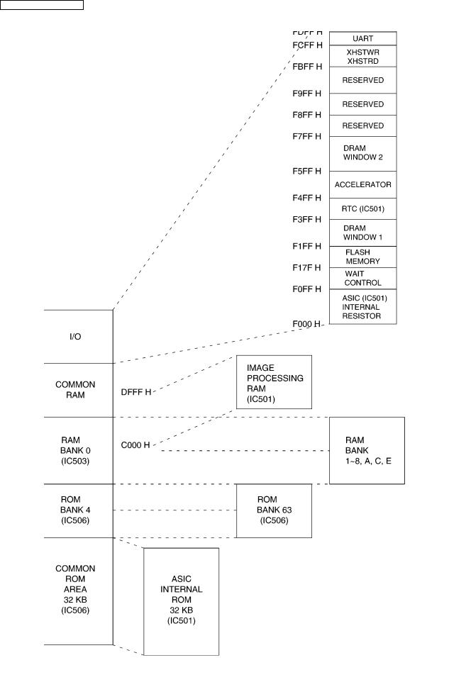
6.3.4.Flash Memory (IC506)
This 512KB ROM (FLASH MEMORY) carries a common area of 32KB and bank areas which each have 8KB (BK4~BK63). The addresses from 0000H to 7FFFH are for the common area and from 8000H to 9FFFH are for the bank areas.
6.3.5.Dynamic RAM (IC503)
The DRAM serves as CPU and receives memory.
The address is F200H~F3FFH (DRAM access window 1) and F600H~F7FFH (DRAM access window 2).
18
KX-FP207FX-S/FP218FX-S
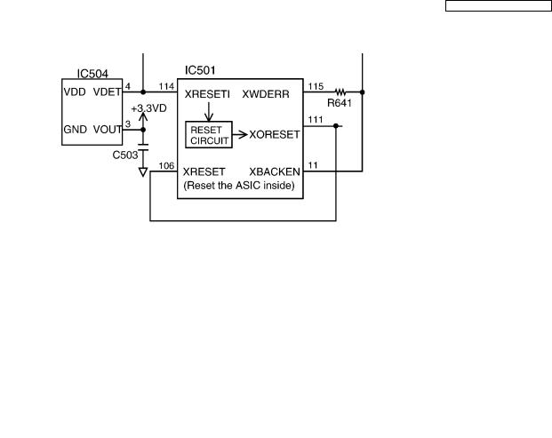
6.3.6.Reset Circuit (Watch dog timer)
The output signal (reset) from pin 4 of the voltage detect IC (IC504) is input to the ASIC (IC501) 114 pin.
1.During a momentary power interruption, a positive reset pulse of 50~70 msec is generated and the system is reset completely.
2.The watch dog timer, built-in the ASIC (IC501), is initialized by the CPU about every 1.5 ms. When a watch dog error occurs, pin 115 of the ASIC (IC501) becomes low level.
The terminal of the 'WDERR' signal is connected to the reset line, so the 'WDERR' signal works as the reset signal.
19
KX-FP207FX-S/FP218FX-S
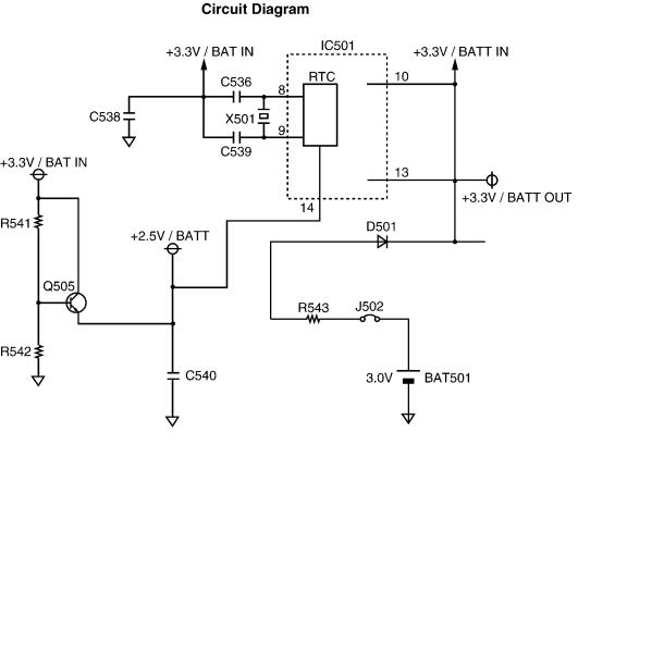
6.3.7.RTC Backup Circuit
1.Function
This unit has a lithium battery (BAT501) which works for Real Time Clock IC (RTC: inside IC501). The RTC continues to work, backed up by a lithium battery even when the power switch is OFF.
The user parameters for autodial numbers, the system setup data and others are in the FLASH MEMORY (IC506).
2.RTC Inside (IC501) Backup Circuit Operation
When the power switch is turned ON, power is supplied through Q505 to the RTC (inside IC501). At this time, the voltage at pin 14 of the IC501 is +2.5V. When the power switch is turned OFF, the BAT501 supplies power to RTC through D501 and Q505. The voltage at pin 14 of IC501 is about +2.2V. When the power switch is OFF and the voltage of +3.3V decreases, pin 14 of RTC (IC501) becomes roughly the same voltage as the battery voltage. RTC goes into the backup mode, in which the power consumption is lower.
20
KX-FP207FX-S/FP218FX-S
6.3.8.Supervision Circuit for the Terminal Head Temperature
1. Function
The thermistor changes the resistor according to the temperature and uses the thermistor's characteristics. The output of pin 139 of IC501 becomes a low level. Then when it becomes a high level, it triggers point A In point C, according to the voltage output time, the thermal head's temperature is detected.
After the thermal head temperature is converted to voltage in B, it is then changed to digital data in the A/D converter inside IC501. The CPU decides the strobe width of the thermal head according to this value. Therefore, this circuit can keep the thermal head at an even temperature in order to stabilize the printing density and prevent the head from being overheated.
REFERENCE:
Thermal Head (P.24)
21

KX-FP207FX-S/FP218FX-S
6.4.Facsimile Section
6.4.1.Image Data Flow During Facsimile Operation
Copy (Fine, Super-Fine, Half Tone)
1.Line information is read by CIS (to be used as the reference white level) via route1, and is input to IC501. Refer to Block Diagram (P.23)
2.In IC501, the data is adjusted to a suitable level for A/D conversion in the Analogue Signal Processing Section, and via route2 it is input to A/D conversion (8 bit). After finishing A/D conversion, the data is input to the Image Processing Section via route3. Then via route4 and route5, it is stored in RAM as shading data.
3.The draft’s information that is read by CIS is input to IC501 via route1. After it is adjusted to a suitable level for A/D conversion via route2, the draft’s information is converted to A/D (8 bit), and it is input to the Image Processing Section. The other side, the shading data which flows from RAM via route6 and route7, is input to the Image Processing Section. After finishing the draft’s information image processing, white is regarded as "0" and black is regarded as "1". Then via routes4 and 5, they are stored in RAM.
4.The white/black data stored as above via routes6 and8 is input to the P/S converter. The white/black data converted to serial data in the P/S converter is input to the Thermal Head via route9 and is printed out on recording paper.
Note:
Standard: Reads 3.85 times/mm
Fine: Reads 7.7 times/mm
Super-Fine: Reads 15.4 times/mm
Transmission
1.Same processing as Copy items 1 - 3.
2.The data stored in the RAM of IC501 is output from IC501 via routes6 and 10, and is stored in the system bus. Via route11, it is stored in the communication buffer inside DRAM (IC503).
3.While retrieving data stored in the communication buffer synchronous with the modem, the CPU (inside IC501) inputs the data
to the modem along route12, where it is converted to serial analogue data and forwarded over the telephone lines via the NCU Section.
Reception
1.The serial analogue image data is received over the telephone lines and input to the modem via the NCU section, where it is demodulated to parallel digital data. Then the CPU (IC501) stores the data in the communication buffer DRAM (IC503) along route12.
2.The data stored in DRAM (IC503) is decoded by the CPU (IC501) via route12, and is stored in DRAM (IC503) via routes13 and 5.
3.Same processing as Copy item 4.
22
KX-FP207FX-S/FP218FX-S
6.4.2.Block Diagram
23
KX-FP207FX-S/FP218FX-S
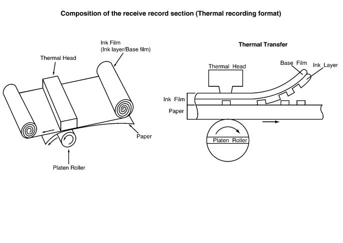
6.4.3.Thermal Head
1.Function
This unit utilizes the state of the art thermal printer technology.
The ink film is chemically processed. The ink film is comprised of two parts: an ink layer and a base film. When the thermalhead contacts this ink film, it emits heat momentarily, and the ink layer is melted and transferred to the paper. If this continues, letters and/or diagrams appear, and the original document is reproduced.
2.Circuit Operation
Refer to the block diagram and the timing chart on the following page.
There are 9 driver ICs aligned horizontally on the thermal head and each one of these ICs can drive 192 heat emitting registers. This means that one line is at a density of 192×9=1728 dots=(8 dots/mm).
White/Black (white=0, black=1) data in one line increments is synchronized at IC501 pin 117 (THCLK), and sent from IC501 pin 116 (THDAT) to the shift register of the ICs. The shift registers of the 9 ICs are connected in series, and upon the shift of dot increment 1728, all the shift registers become filled with data, and a latch pulse is emitted to each IC from IC501 pin 118 (THLAT).With this latch pulse, all the contents of the shift registers are latched to the latch registers. Thereafter, through the addition of strobes from the IC501 pins (103, 104) only black dot locations (=1) among latched data activates the driver, and the current passes to heat the emitting body causing heat emission.
Here, the two line strobes, STB1 and STB2, impress at intervals of 9.216 msec, as required for one-line printout.
The sequence is shown on the next page. [Moreover, for the strobe width, the thermistor value inside the thermal head is detected according to IC501 pin 4. Depending on that value, the strobe width is recorded in ROM (IC506).
Accordingly, the strobe width is determined.
When the thermal head is not used, the IC501 (17, THON) becomes low, Q502 turns OFF, Q401 turns OFF, and the +24 V power supply for the thermal head driver is not impressed to protect the IC.
24

KX-FP207FX-S/FP218FX-S
25
KX-FP207FX-S/FP218FX-S
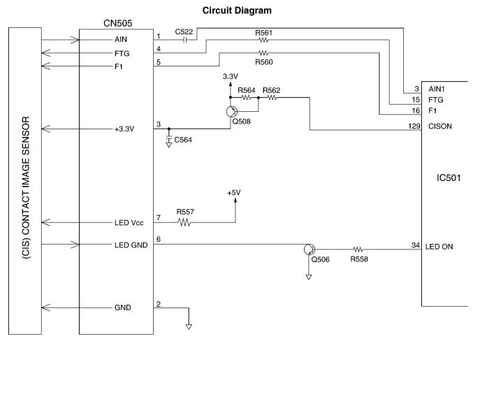
6.4.4.Scanning Block
The scanning block of this device consists of a control circuit and a contact image sensor made up of a celfoc lens array, an LED array, and photoelectric conversion elements.
When an original document is inserted and the start button pressed, pin 34 of IC501 goes to a high level and the transistor Q506 turns on.This applies voltage to the LED array to light it. The contact image sensor is driven by each of the FTG-F1 signals output from IC501, and the original image illuminated by the LED array undergoes photoelectric conversion to output an analogue image signal (AIN). The analogue image signal is input to the system ASIC on AIN1 (pin 3 of IC501) and converted into 8-bit data by the A/ D converter inside IC501. Then this signal undergoes digital processing in order to obtain a high-quality image.
26
KX-FP207FX-S/FP218FX-S
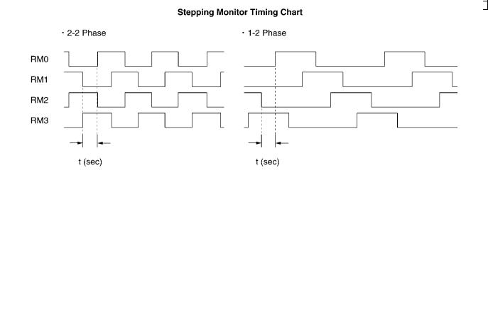
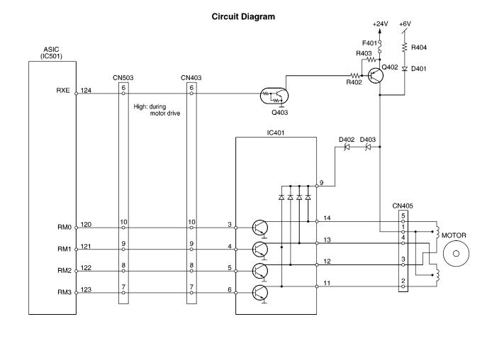
6.4.5.Stepping Motor Drive Circuit
1.Function
The stepping motor works for both transmission and reception.
2.Motor
During motor driving, pin 124 of ASIC IC501 becomes a high level, and Q403, Q402 turns ON. As a result, +24V is supplied to
the motor coil.
Stepping pulses are output from ASIC IC501 pins, 124, 120~123, causing driver IC401 pins, 14~11 to drive the Motor Coil. The motor coil is energized sequentially in 2 phase increments, which causes a 1-step rotation. A 1-step rotation feeds 0.13 mm of recording paper or document paper.
The timing chart is below.
Stepping Motor Drive Mode
Function |
Mode |
Phase Pattern |
Speed |
|
|
|
|
|
|
Copy |
Fine, Photo |
1-2 |
432 pps (t=1/432) |
|
|
|
|
|
|
|
|
Super Fine |
1-2 |
216 pps (t=1/216) |
FAX Sending |
Standard |
2-2 |
432 pps (t=1/432) |
|
|
|
Fine, Photo |
1-2 |
432 pps (t=1/432) |
|
|
|
|
|
|
|
Super Fine |
1-2 |
216 pps (t=1/216) |
|
|
|
|
|
FAX Receiving |
Standard, Fine, Photo |
1-2 |
432 pps (t=1/432) |
|
|
|
|
|
|
|
|
Super Fine |
1-2 |
216 pps (t=1/216) |
Paper Feed |
——— |
1-2 |
432 pps (t=1/432) |
|
Document Feed |
——— |
1-2 |
432 pps (t=1/432) |
|
|
|
|
|
|
Stand-by |
——— |
All phases are currently off. |
None |
|
|
|
|
|
|
27
KX-FP207FX-S/FP218FX-S
When the motor suspends while it is in the receive mode (about 70~80 msec), pin 124 of ASIC IC501 becomes a low level and Q403 turns OFF. Then Q402 also turns OFF, and instead of +24 V, +6 V is supplied through D401 so that the motor is held in place. When the system is in the stand-by mode, all of the motor drive transistors turn OFF. Consequently, the motor current stops.
28
KX-FP207FX-S/FP218FX-S
6.5.Sensors and Switches
All of the sensor and switches are shown below.
Sensor Circuit Location |
Sensor |
Sensor or Switch Name |
Error Message |
Operation Panel |
SW351 |
Document top sensor |
[REMOVE DOCUMENT] |
|
|
|
|
|
SW352 |
Document set sensor |
[CHECK DOCUMENT] |
|
|
|
|
Sensor P.C.Board |
SW1001 |
Cover Open sensor |
[CHECK COVER] |
|
|
Paper Top sensor |
[PAPER JAMMED] |
|
SW1002 |
Film Detection sensor |
[FILM EMPTY] |
Film End Sensor P.C.Board |
SW1003 |
Film End sensor |
[CHECK FILM] |
|
|
|
|
Gear Block |
SW1004 |
Motor Position sensor |
[CALL SERVICE2] |
|
|
|
|
HOOK SW P.C.Board |
SW1501 |
Hook switch |
———— |
Note:
See Test Mode (P.58). (#815: Sensor Check)
Sensor Locations
29
KX-FP207FX-S/FP218FX-S
6.5.1.Document Top Sensor (SW351)
When a document is brought to the read position, the SW turns ON, and the input signal of IC301-6 pin (Operation Board) becomes a low level. When there is no document at the read position, the SW turns OFF, and the input signal of IC301-6 pin (Operation Board) becomes a high level.
|
SW |
Signal (IC301-6 pin) |
Out of the Read Position |
OFF |
High level |
At the Read Position |
ON |
Low level |
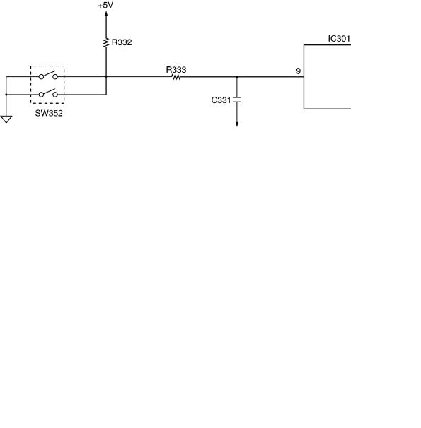
6.5.2.Document Set Sensor (SW352)
When a document is set, the SW turns ON, and the input signal of IC301-9 pin (Operation Board) becomes a low level. When there is no document, the SW turns ON, and the input signal of IC301-9 pin (Operation Board) becomes a high level.
|
SW |
Signal (IC301-9 pin) |
No document |
OFF |
High level |
Set document |
ON |
Low level |
|
|
|
30
Loading...