


MSM5117405B-60TS-K
OKI MSM5117405B-60TS-K, MSM5117405B-50TS-K, MSM5117405B-70TS-L, MSM5117405B-60TS-L, MSM5117405B-50TS-L Datasheet
...
231
¡ Semiconductor MSM5117405B
DESCRIPTION
The MSM5117405B is a 4,194,304-word ¥ 4-bit dynamic RAM fabricated in Oki's silicon-gate CMOS
technology. The MSM5117405B achieves high integration, high-speed operation, and low-power
consumption because Oki manufactures the device in a quadruple-layer polysilicon/double-layer
metal CMOS process. The MSM5117405B is available in a 26/24-pin plastic SOJ or 26/24-pin plastic
TSOP.
FEATURES
• 4,194,304-word ¥ 4-bit configuration
• Single 5 V power supply, ±10% tolerance
• Input : TTL compatible, low input capacitance
• Output : TTL compatible, 3-state
• Refresh : 2048 cycles/32 ms
• Fast page mode with EDO, read modify write capability
• CAS before RAS refresh, hidden refresh, RAS-only refresh capability
• Multi-bit test mode capability
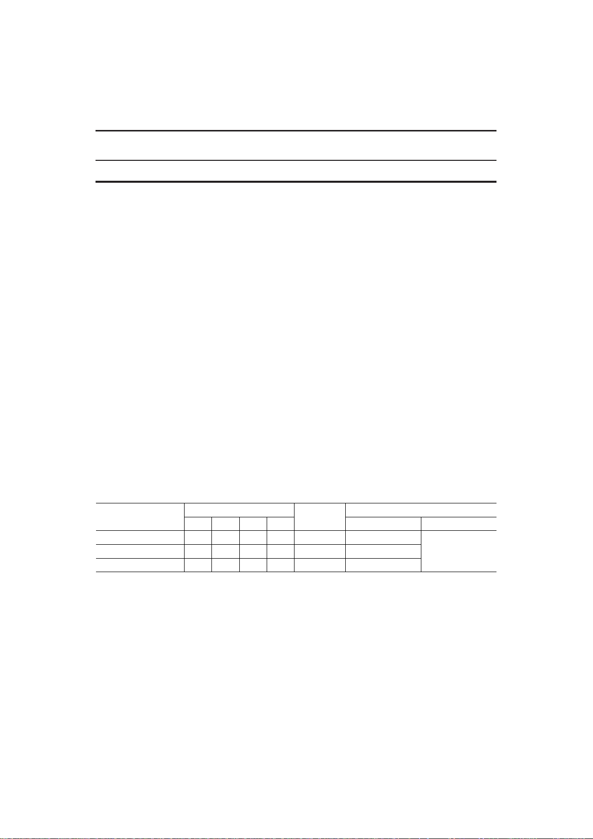
• Package options:
26/24-pin 300 mil plastic SOJ (SOJ26/24-P-300-1.27) (Product : MSM5117405B-xxSJ)
26/24-pin 300 mil plastic TSOP
(TSOPII26/24-P-300-1.27-K)
(Product : MSM5117405B-xxTS-K)
(TSOPII26/24-P-300-1.27-L)
(Product : MSM5117405B-xxTS-L)
xx indicates speed rank.
PRODUCT FAMILY
¡ Semiconductor
MSM5117405B
4,194,304-Word ¥ 4-Bit DYNAMIC RAM : FAST PAGE MODE TYPE WITH EDO
MSM5117405B-70
70 ns
130 ns
90 ns
550 mW
660 mW
Family
Access Time (Max.)
Cycle Time
(Min.)
Standby (Max.)
Power Dissipation
MSM5117405B-50
t
RAC
50 ns
35 ns
t
AA
25 ns
20 ns
t
CAC
13 ns
20 ns
t
OEA
13 ns
MSM5117405B-60
60 ns
110 ns 605 mW
30 ns 15 ns 15 ns
Operating (Max.)
5.5 mW
E2G0039-17-41
232
MSM5117405B ¡ Semiconductor
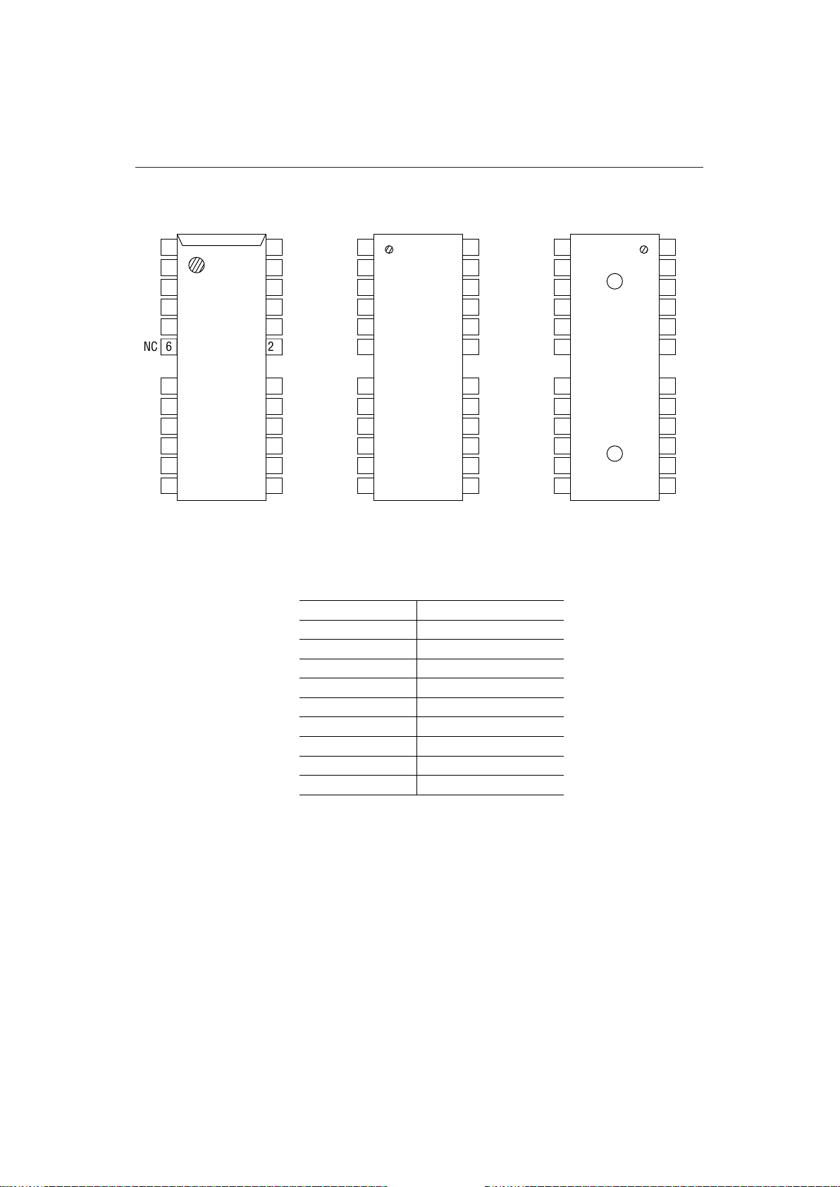
PIN CONFIGURATION (TOP VIEW)
26/24-Pin Plastic SOJ 26/24-Pin Plastic TSOP
(K Type)
26/24-Pin Plastic TSOP
(L Type)
Pin Name Function
A0 - A10
Address Input
RAS Row Address Strobe
CAS Column Address Strobe
DQ1 - DQ4 Data Input/Data Output
OE Output Enable
WE Write Enable
V
CC
Power Supply (5 V)
V
SS
Ground (0 V)
3
4
5
9
10
11
12
13
DQ2
A0
A1
A2
A3
V
CC
24
23
22
18
17
16
15
14
DQ3
A7
A6
A5
A4
V
SS
2DQ1 25 DQ4
1
V
CC
26 V
SS
3
4
5
9
10
11
12
13
24
23
22
18
17
16
15
14
2
25
1
26
24
23
22
18
17
16
15
14
3
4
5
9
10
11
12
13
25
2
26
1
6NC 21 A9 21 21 6
8A10 19 A8 19 19 8
6
8
DQ2
A0
A1
A2
A3
V
CC
DQ1
V
CC
NC
A10
DQ3
A7
A6
A5
A4
V
SS
DQ4
V
SS
A9
A8
DQ3
A7
A6
A5
A4
V
SS
DQ4
V
SS
A9
A8
DQ2
A0
A1
A2
A3
V
CC
DQ1
V
CC
NC
A10
WE CAS WE CAS CAS WE
RAS OE RAS OE OE RAS
NC No Connection
Note : The same power supply voltage must be provided to every V
CC
pin, and the same GND
voltage level must be provided to every V
SS
pin.
233
¡ Semiconductor MSM5117405B
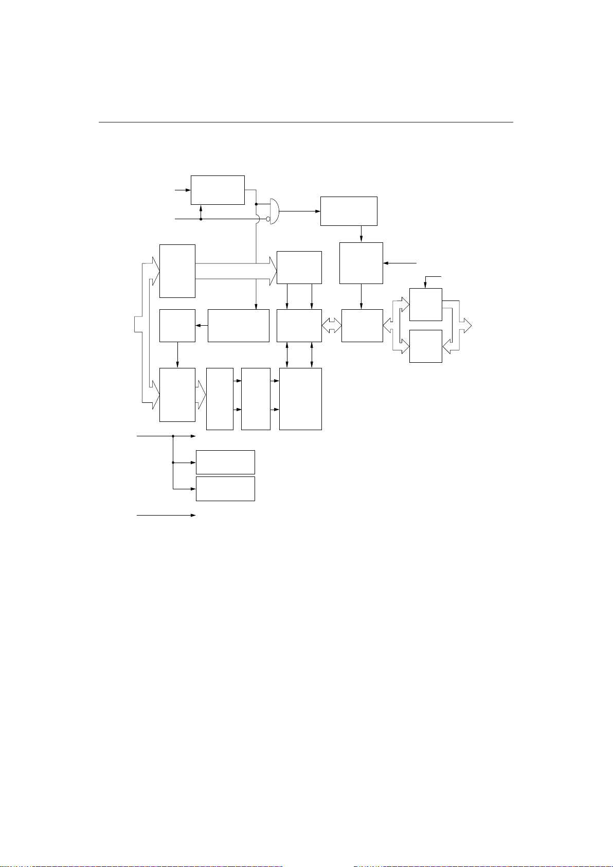
BLOCK DIAGRAM
Timing
Generator
RAS
CAS
Timing
Generator
Internal
Address
Counter
Row
Address
Buffers
Row
De-
coders
Word
Drivers
Memory
Cells
Refresh
Control Clock
Sense
Amplifiers
Column
Decoders
Write
Clock
Generator
I/O
Selector
Output
Buffers
WE
OE
4
DQ1 - DQ4
4
4
4
4
4
Input
Buffers
4
11
A0 - A10
11
1111
Column
Address
Buffers
V
CC
V
SS
On Chip
IV
CC
Generator
On Chip
V
BB
Generator
 Loading...