


 Loading...
NEC PD78F0500, PD78F0500-A, PD78F0500-A2, PD78F0501, PD78F0501-A User Manual
...User’s Manual
78K0/KB2
8-Bit Single-Chip Microcontrollers
PD78F0500 PD78F0500(A) PD78F0500(A2)PD78F0501 PD78F0501(A) PD78F0501(A2)PD78F0502 PD78F0502(A) PD78F0502(A2)PD78F0503 PD78F0503(A) PD78F0503(A2)PD78F0503D
The PD78F0503D has an on-chip debug function.
Do not use this product for mass production because its reliability cannot be guaranteed after the on-chip debug function has been used, due to issues with respect to the number of times the flash memory can be rewritten. NEC Electronics does not accept complaints concerning this product.
Document No. U17328EJ5V0UD00 (5th edition)
Date Published July 2007 NS
2006
Printed in Japan
[MEMO]
2
User’s Manual U17328EJ5V0UD

NOTES FOR CMOS DEVICES
1VOLTAGE APPLICATION WAVEFORM AT INPUT PIN
Waveform distortion due to input noise or a reflected wave may cause malfunction. If the input of the CMOS device stays in the area between VIL (MAX) and VIH (MIN) due to noise, etc., the device may malfunction. Take care to prevent chattering noise from entering the device when the input level is fixed, and also in the transition period when the input level passes through the area between VIL (MAX) and VIH (MIN).
2HANDLING OF UNUSED INPUT PINS
Unconnected CMOS device inputs can be cause of malfunction. If an input pin is unconnected, it is possible that an internal input level may be generated due to noise, etc., causing malfunction. CMOS devices behave differently than Bipolar or NMOS devices. Input levels of CMOS devices must be fixed high or low by using pull-up or pull-down circuitry. Each unused pin should be connected to VDD or GND via a resistor if there is a possibility that it will be an output pin. All handling related to unused pins must be judged separately for each device and according to related specifications governing the device.
3PRECAUTION AGAINST ESD
A strong electric field, when exposed to a MOS device, can cause destruction of the gate oxide and ultimately degrade the device operation. Steps must be taken to stop generation of static electricity as much as possible, and quickly dissipate it when it has occurred. Environmental control must be adequate. When it is dry, a humidifier should be used. It is recommended to avoid using insulators that easily build up static electricity. Semiconductor devices must be stored and transported in an anti-static container, static shielding bag or conductive material. All test and measurement tools including work benches and floors should be grounded. The operator should be grounded using a wrist strap. Semiconductor devices must not be touched with bare hands. Similar precautions need to be taken for PW boards with mounted semiconductor devices.
4STATUS BEFORE INITIALIZATION
Power-on does not necessarily define the initial status of a MOS device. Immediately after the power source is turned ON, devices with reset functions have not yet been initialized. Hence, power-on does not guarantee output pin levels, I/O settings or contents of registers. A device is not initialized until the reset signal is received. A reset operation must be executed immediately after power-on for devices with reset functions.
5POWER ON/OFF SEQUENCE
In the case of a device that uses different power supplies for the internal operation and external interface, as a rule, switch on the external power supply after switching on the internal power supply. When switching the power supply off, as a rule, switch off the external power supply and then the internal power supply. Use of the reverse power on/off sequences may result in the application of an overvoltage to the internal elements of the device, causing malfunction and degradation of internal elements due to the passage of an abnormal current.
The correct power on/off sequence must be judged separately for each device and according to related specifications governing the device.
6INPUT OF SIGNAL DURING POWER OFF STATE
Do not input signals or an I/O pull-up power supply while the device is not powered. The current injection that results from input of such a signal or I/O pull-up power supply may cause malfunction and the abnormal current that passes in the device at this time may cause degradation of internal elements. Input of signals during the power off state must be judged separately for each device and according to related specifications governing the device.
User’s Manual U17328EJ5V0UD |
3 |
EEPROM is a trademark of NEC Electronics Corporation.
Windows and Windows NT are registered trademarks or trademarks of Microsoft Corporation in the United States and/or other countries.
PC/AT is a trademark of International Business Machines Corporation.
HP9000 series 700 and HP-UX are trademarks of Hewlett-Packard Company.
SPARCstation is a trademark of SPARC International, Inc.
Solaris and SunOS are trademarks of Sun Microsystems, Inc.
SuperFlash is a registered trademark of Silicon Storage Technology, Inc. in several countries including the United States and Japan.
4 |
User’s Manual U17328EJ5V0UD |

Caution: This product uses SuperFlash® technology licensed from Silicon Storage Technology, Inc.
•The information in this document is current as of July, 2007. The information is subject to change without notice. For actual design-in, refer to the latest publications of NEC Electronics data sheets or data books, etc., for the most up-to-date specifications of NEC Electronics products. Not all products and/or types are available in every country. Please check with an NEC Electronics sales representative for availability and additional information.
•No part of this document may be copied or reproduced in any form or by any means without the prior written consent of NEC Electronics. NEC Electronics assumes no responsibility for any errors that may appear in this document.
•NEC Electronics does not assume any liability for infringement of patents, copyrights or other intellectual property rights of third parties by or arising from the use of NEC Electronics products listed in this document or any other liability arising from the use of such products. No license, express, implied or otherwise, is granted under any patents, copyrights or other intellectual property rights of NEC Electronics or others.
•Descriptions of circuits, software and other related information in this document are provided for illustrative purposes in semiconductor product operation and application examples. The incorporation of these circuits, software and information in the design of a customer's equipment shall be done under the full responsibility of the customer. NEC Electronics assumes no responsibility for any losses incurred by customers or third parties arising from the use of these circuits, software and information.
•While NEC Electronics endeavors to enhance the quality, reliability and safety of NEC Electronics products, customers agree and acknowledge that the possibility of defects thereof cannot be eliminated entirely. To minimize risks of damage to property or injury (including death) to persons arising from defects in NEC Electronics products, customers must incorporate sufficient safety measures in their design, such as redundancy, fire-containment and anti-failure features.
•NEC Electronics products are classified into the following three quality grades: "Standard", "Special" and "Specific".
The "Specific" quality grade applies only to NEC Electronics products developed based on a customerdesignated "quality assurance program" for a specific application. The recommended applications of an NEC Electronics product depend on its quality grade, as indicated below. Customers must check the quality grade of each NEC Electronics product before using it in a particular application.
"Standard": Computers, office equipment, communications equipment, test and measurement equipment, audio and visual equipment, home electronic appliances, machine tools, personal electronic equipment and industrial robots.
"Special": Transportation equipment (automobiles, trains, ships, etc.), traffic control systems, anti-disaster systems, anti-crime systems, safety equipment and medical equipment (not specifically designed for life support).
"Specific": Aircraft, aerospace equipment, submersible repeaters, nuclear reactor control systems, life support systems and medical equipment for life support, etc.
The quality grade of NEC Electronics products is "Standard" unless otherwise expressly specified in NEC Electronics data sheets or data books, etc. If customers wish to use NEC Electronics products in applications not intended by NEC Electronics, they must contact an NEC Electronics sales representative in advance to determine NEC Electronics' willingness to support a given application.
(Note)
(1)"NEC Electronics" as used in this statement means NEC Electronics Corporation and also includes its majority-owned subsidiaries.
(2)"NEC Electronics products" means any product developed or manufactured by or for NEC Electronics (as defined above).
M8E |
02. 11-1 |
User’s Manual U17328EJ5V0UD |
5 |
|
INTRODUCTION |
|
|
||
Readers |
This manual is intended for user engineers who wish to understand the functions of the |
||||
|
78K0/KB2 and design and develop application systems and programs for these devices. |
||||
|
The target products are as follows. |
|
|
||
|
78K0/KB2: PD78F0500, 78F0501, 78F0502, 78F0503, 78F0503D, |
||||
|
78F0500(A), 78F0501(A), 78F0502(A), 78F0503(A), |
||||
<R> |
78F0500(A2), 78F0501(A2), 78F0502(A2), 78F0503(A2) |
||||
|
|||||
Purpose |
This manual is intended to give users an understanding of the functions described in the |
||||
|
Organization below. |
|
|
||
Organization |
The 78K0/KB2 manual is separated into two parts: |
this manual and the instructions |
|||
|
edition (common to 78K0 microcontrollers). |
|
|
||
|
|
|
|
|
|
|
78K0/KB2 |
|
|
78K/0 Series |
|
|
User’s Manual |
|
|
User’s Manual |
|
|
(This Manual) |
|
|
Instructions |
|
|
|
|
|
|
|
|
|
|
|
|
|
•Pin functions
•Internal block functions
•Interrupts
•Other on-chip peripheral functions
•Electrical specifications
•CPU functions
•Instruction set
•Explanation of each instruction
How to Read This Manual It is assumed that the readers of this manual have general knowledge of electrical |
|
|
engineering, logic circuits, and microcontrollers. |
<R> |
• When using this manual as the manual for (A) grade products and (A2) grade |
|
products : |
|
→ Only the quality grade differs between standard products and (A) grade products, |
|
and (A2) grade products. Read the part number as follows. |
|
• PD78F0500→ PD78F0500(A), 78F0500(A2) |
|
• PD78F0501→ PD78F0501(A), 78F0501(A2) |
|
• PD78F0502→ PD78F0502(A), 78F0502(A2) |
|
• PD78F0503→ PD78F0503(A), 78F0503(A2) |
|
• To gain a general understanding of functions: |
|
→ Read this manual in the order of the CONTENTS. The mark “<R>” shows major |
|
revised points. The revised points can be easily searched by copying an “<R>” in |
|
the PDF file and specifying it in the “Find what:” field. |
|
• How to interpret the register format: |
|
→ For a bit number enclosed in angle brackets, the bit name is defined as a |
|
reserved word in the RA78K0, and is defined as an sfr variable using the |
|
#pragma sfr directive in the CC78K0. |
|
• To check the details of a register when you know the register name: |
|
→ See APPENDIX C REGISTER INDEX. |
6 |
User’s Manual U17328EJ5V0UD |
•To know details of the 78K/0 Series instructions:
→Refer to the separate document 78K/0 Series Instructions User’s Manual (U12326E).
Conventions |
Data significance: |
Higher digits on the left and lower digits on the right |
||
|
Active low representations: |
|
(overscore over pin and signal name) |
|
|
××× |
|||
|
Note: |
Footnote for item marked with Note in the text |
||
|
Caution: |
Information requiring particular attention |
||
|
Remark: |
Supplementary information |
||
|
Numerical representations: |
Binary |
... ×××× or ××××B |
|
|
|
Decimal |
... ×××× |
|
|
|
Hexadecimal |
... ××××H |
|
Related Documents |
The related documents indicated in this publication may include preliminary versions. |
|||
However, preliminary versions are not marked as such.
Documents Related to Devices
|
Document Name |
Document No. |
|
|
|
|
78K0/KB2 User’s Manual |
This manual |
|
|
|
|
78K/0 Series Instructions User’s Manual |
U12326E |
|
|
|
|
78K0/Kx2 Flash Memory Programming (Programmer) Application Note |
U17739E |
|
|
|
|
78K0/Kx2 Flash Memory Self Programming User’s ManualNote |
U17516E |
<R> |
|
|
78K0/Kx2 EEPROM™ Emulation Application Note Note |
U17517E |
|
|
|
|
Note This document is under engineering management. For details, consult an NEC Electronics sales representative.
Documents Related to Development Tools (Software) (User’s Manuals)
|
Document Name |
Document No. |
|
|
|
|
|
RA78K0 Ver. 3.80 Assembler Package |
|
Operation |
U17199E |
|
|
|
|
|
|
Language |
U17198E |
|
|
|
|
|
|
Structured Assembly Language |
U17197E |
|
|
|
|
CC78K0 Ver. 3.70 C Compiler |
|
Operation |
U17201E |
|
|
|
|
|
|
Language |
U17200E |
|
|
|
|
SM+ System Simulator |
|
Operation |
U17246E |
|
|
|
|
|
|
External Part User Open Interface |
U17247E |
|
|
Specifications |
|
|
|
|
|
ID78K0-QB Ver. 2.90 Integrated Debugger |
|
Operation |
U17437E |
|
|
|
|
PM+ Ver. 5.20 |
|
|
U16934E |
|
|
|
|
Caution The related documents listed above are subject to change without notice. Be sure to use the latest
version of each document when designing.
User’s Manual U17328EJ5V0UD |
7 |
Documents Related to Development Tools (Hardware) (User’s Manuals)
|
Document Name |
Document No. |
|
|
|
|
QB-78K0KX2 In-Circuit Emulator |
U17341E |
|
|
|
|
QB-78K0MINI On-Chip Debug Emulator |
U17029E |
<R> |
|
|
QB-MINI2 On-Chip Debug Emulator with Programming Function |
U18371E |
|
|
|
|
|
Documents Related to Flash Memory Programming (User’s Manuals) |
|
|
|
|
|
Document Name |
Document No. |
|
|
|
|
PG-FP4 Flash Memory Programmer |
U15260E |
|
|
|
|
PG-FPL3 Flash Memory Programmer |
U17454E |
|
|
|
|
Other Documents |
|
|
|
|
|
Document Name |
Document No. |
|
|
|
|
SEMICONDUCTOR SELECTION GUIDE − Products and Packages − |
X13769X |
|
|
|
|
Semiconductor Device Mount Manual |
Note |
|
|
|
|
Quality Grades on NEC Semiconductor Devices |
C11531E |
|
|
|
|
NEC Semiconductor Device Reliability/Quality Control System |
C10983E |
|
|
|
|
Guide to Prevent Damage for Semiconductor Devices by Electrostatic Discharge (ESD) |
C11892E |
|
|
|
Note See the “Semiconductor Device Mount Manual” website (http://www.necel.com/pkg/en/mount/index.html).
Caution The related documents listed above are subject to change without notice. Be sure to use the latest version of each document when designing.
8 |
User’s Manual U17328EJ5V0UD |
CONTENTS
CHAPTER 1 OUTLINE ............................................................................................................................ |
16 |
|
1.1 |
Features ........................................................................................................................................ |
16 |
1.2 |
Applications.................................................................................................................................. |
17 |
1.3 |
Ordering Information ................................................................................................................... |
18 |
1.4 |
Pin Configuration (Top View)...................................................................................................... |
19 |
1.5 |
78K0/Kx2 Microcontroller Lineup............................................................................................... |
22 |
1.6 |
Block Diagram .............................................................................................................................. |
25 |
1.7 |
Outline of Functions .................................................................................................................... |
26 |
CHAPTER 2 PIN FUNCTIONS............................................................................................................... |
28 |
|
2.1 |
Pin Function List .......................................................................................................................... |
28 |
2.2 |
Description of Pin Functions ...................................................................................................... |
31 |
User’s Manual U17328EJ5V0UD |
9 |
3.4 Operand Address Addressing .................................................................................................... |
65 |
|
3.4.1 |
Implied addressing .......................................................................................................................... |
65 |
3.4.2 |
Register addressing ........................................................................................................................ |
66 |
3.4.3 |
Direct addressing ............................................................................................................................ |
67 |
3.4.4 |
Short direct addressing ................................................................................................................... |
68 |
3.4.5 |
Special function register (SFR) addressing..................................................................................... |
69 |
3.4.6 |
Register indirect addressing............................................................................................................ |
70 |
3.4.7 |
Based addressing ........................................................................................................................... |
71 |
3.4.8 |
Based indexed addressing.............................................................................................................. |
72 |
3.4.9 |
Stack addressing............................................................................................................................. |
73 |
CHAPTER 4 |
PORT FUNCTIONS ........................................................................................................... |
74 |
||
4.1 |
Port Functions .............................................................................................................................. |
74 |
||
4.2 |
Port Configuration........................................................................................................................ |
75 |
||
|
4.2.1 |
Port 0 .............................................................................................................................................. |
76 |
|
|
4.2.2 |
Port 1 .............................................................................................................................................. |
78 |
|
|
4.2.3 |
Port 2 .............................................................................................................................................. |
83 |
|
|
4.2.4 |
Port 3 .............................................................................................................................................. |
84 |
|
|
4.2.5 |
Port 6 .............................................................................................................................................. |
87 |
|
|
4.2.6 |
Port 12 ............................................................................................................................................ |
88 |
|
4.3 |
Registers Controlling Port Function .......................................................................................... |
91 |
||
4.4 |
Port Function Operations ............................................................................................................ |
96 |
||
|
4.4.1 |
Writing to I/O port ............................................................................................................................ |
96 |
|
|
4.4.2 |
Reading from I/O port...................................................................................................................... |
96 |
|
|
4.4.3 |
Operations on I/O port..................................................................................................................... |
96 |
|
4.5 |
Settings of Port Mode Register and Output Latch When Using Alternate Function............. |
97 |
||
4.6 |
Cautions on 1-Bit Manipulation Instruction for Port Register n (Pn)...................................... |
99 |
||
CHAPTER 5 |
CLOCK GENERATOR .................................................................................................... |
100 |
||
5.1 |
Functions of Clock Generator................................................................................................... |
100 |
||
5.2 |
Configuration of Clock Generator ............................................................................................ |
101 |
||
5.3 |
Registers Controlling Clock Generator.................................................................................... |
103 |
||
5.4 |
System Clock Oscillator ............................................................................................................ |
111 |
||
|
5.4.1 |
X1 oscillator.................................................................................................................................... |
111 |
|
|
5.4.2 |
Internal high-speed oscillator ......................................................................................................... |
113 |
|
|
5.4.3 |
Internal low-speed oscillator........................................................................................................... |
113 |
|
|
5.4.4 |
Prescaler........................................................................................................................................ |
113 |
|
5.5 |
Clock Generator Operation ....................................................................................................... |
114 |
||
5.6 |
Controlling Clock........................................................................................................................ |
117 |
||
|
5.6.1 |
Example of controlling high-speed system clock............................................................................ |
117 |
|
|
5.6.2 |
Example of controlling internal high-speed oscillation clock........................................................... |
120 |
|
|
5.6.3 |
Example of controlling internal low-speed oscillation clock ............................................................ |
122 |
|
|
5.6.4 |
Clocks supplied to CPU and peripheral hardware.......................................................................... |
123 |
|
|
5.6.5 |
CPU clock status transition diagram .............................................................................................. |
124 |
|
|
5.6.6 |
Condition before changing CPU clock and processing after changing CPU clock ......................... |
127 |
|
|
5.6.7 |
Time required for switchover of main system clock........................................................................ |
128 |
|
|
5.6.8 |
Conditions before clock oscillation is stopped................................................................................ |
129 |
|
|
5.6.9 |
Peripheral hardware and source clocks ......................................................................................... |
129 |
|
10 |
|
|
User’s Manual U17328EJ5V0UD |
|
CHAPTER 6 16-BIT TIMER/EVENT COUNTER 00........................................................................... |
130 |
||
6.1 |
Functions of 16-bit Timer/Event Counter 00 ........................................................................... |
130 |
|
6.2 |
Configuration of 16-bit Timer/Event Counter 00..................................................................... |
131 |
|
6.3 |
Registers Controlling 16-bit Timer/Event Counter 00 ............................................................ |
136 |
|
6.4 |
Operation of 16-bit Timer/Event Counter 00............................................................................ |
144 |
|
|
6.4.1 |
Interval timer operation .................................................................................................................. |
144 |
|
6.4.2 |
Square wave output operation ....................................................................................................... |
147 |
|
6.4.3 |
External event counter operation ................................................................................................... |
150 |
|
6.4.4 |
Operation in clear & start mode entered by TI000 pin valid edge input.......................................... |
153 |
|
6.4.5 |
Free-running timer operation ......................................................................................................... |
166 |
|
6.4.6 |
PPG output operation .................................................................................................................... |
175 |
|
6.4.7 |
One-shot pulse output operation.................................................................................................... |
178 |
|
6.4.8 |
Pulse width measurement operation.............................................................................................. |
183 |
6.5 |
Special Use of TM00 .................................................................................................................. |
191 |
|
|
6.5.1 |
Rewriting CR010 during TM00 operation....................................................................................... |
191 |
|
6.5.2 Setting LVS00 and LVR00 ............................................................................................................. |
191 |
|
6.6 |
Cautions for 16-bit Timer/Event Counter 00............................................................................ |
193 |
|
CHAPTER 7 8-BIT TIMER/EVENT COUNTERS 50 AND 51 .......................................................... |
197 |
||
7.1 |
Functions of 8-bit Timer/Event Counters 50 and 51............................................................... |
197 |
|
7.2 |
Configuration of 8-bit Timer/Event Counters 50 and 51 ........................................................ |
197 |
|
7.3 |
Registers Controlling 8-bit Timer/Event Counters 50 and 51................................................ |
200 |
|
7.4 |
Operations of 8-bit Timer/Event Counters 50 and 51 ............................................................. |
205 |
|
|
7.4.1 |
Operation as interval timer............................................................................................................. |
205 |
|
7.4.2 |
Operation as external event counter .............................................................................................. |
207 |
|
7.4.3 |
Square-wave output operation....................................................................................................... |
208 |
|
7.4.4 PWM output operation ................................................................................................................... |
209 |
|
7.5 |
Cautions for 8-bit Timer/Event Counters 50 and 51 ............................................................... |
213 |
|
CHAPTER 8 8-BIT TIMERS H0 AND H1 .......................................................................................... |
214 |
||
8.1 |
Functions of 8-bit Timers H0 and H1 ....................................................................................... |
214 |
|
8.2 |
Configuration of 8-bit Timers H0 and H1 ................................................................................. |
214 |
|
8.3 |
Registers Controlling 8-bit Timers H0 and H1 ........................................................................ |
218 |
|
8.4 |
Operation of 8-bit Timers H0 and H1........................................................................................ |
224 |
|
|
8.4.1 |
Operation as interval timer/square-wave output ............................................................................ |
224 |
|
8.4.2 Operation as PWM output.............................................................................................................. |
227 |
|
|
8.4.3 |
Carrier generator operation (8-bit timer H1 only) ........................................................................... |
233 |
CHAPTER 9 WATCHDOG TIMER ....................................................................................................... |
240 |
||
9.1 |
Functions of Watchdog Timer .................................................................................................. |
240 |
|
9.2 |
Configuration of Watchdog Timer............................................................................................ |
240 |
|
9.3 |
Register Controlling Watchdog Timer ..................................................................................... |
242 |
|
9.4 |
Operation of Watchdog Timer................................................................................................... |
243 |
|
|
9.4.1 |
Controlling operation of watchdog timer......................................................................................... |
243 |
|
9.4.2 |
Setting overflow time of watchdog timer ........................................................................................ |
244 |
|
9.4.3 |
Setting window open period of watchdog timer.............................................................................. |
245 |
|
|
User’s Manual U17328EJ5V0UD |
11 |
CHAPTER 10 |
A/D CONVERTER ......................................................................................................... |
247 |
|
10.1 |
Function of A/D Converter....................................................................................................... |
247 |
|
10.2 |
Configuration of A/D Converter .............................................................................................. |
248 |
|
10.3 |
Registers Used in A/D Converter............................................................................................ |
250 |
|
10.4 |
A/D Converter Operations ....................................................................................................... |
259 |
|
|
10.4.1 |
Basic operations of A/D converter................................................................................................ |
259 |
|
10.4.2 |
Input voltage and conversion results............................................................................................ |
261 |
|
10.4.3 |
A/D converter operation mode ..................................................................................................... |
262 |
10.5 |
How to Read A/D Converter Characteristics Table............................................................... |
264 |
|
10.6 |
Cautions for A/D Converter ..................................................................................................... |
266 |
|
CHAPTER 11 |
SERIAL INTERFACE UART0 ...................................................................................... |
270 |
|
11.1 |
Functions of Serial Interface UART0...................................................................................... |
270 |
|
11.2 |
Configuration of Serial Interface UART0 ............................................................................... |
271 |
|
11.3 |
Registers Controlling Serial Interface UART0....................................................................... |
274 |
|
11.4 |
Operation of Serial Interface UART0 ...................................................................................... |
279 |
|
|
11.4.1 Operation stop mode.................................................................................................................... |
279 |
|
|
11.4.2 |
Asynchronous serial interface (UART) mode ............................................................................... |
280 |
|
11.4.3 |
Dedicated baud rate generator..................................................................................................... |
286 |
|
11.4.4 |
Calculation of baud rate ............................................................................................................... |
287 |
CHAPTER 12 |
SERIAL INTERFACE UART6 ...................................................................................... |
291 |
|
12.1 |
Functions of Serial Interface UART6...................................................................................... |
291 |
|
12.2 |
Configuration of Serial Interface UART6 ............................................................................... |
295 |
|
12.3 |
Registers Controlling Serial Interface UART6....................................................................... |
298 |
|
12.4 |
Operation of Serial Interface UART6 ...................................................................................... |
307 |
|
|
12.4.1 Operation stop mode.................................................................................................................... |
307 |
|
|
12.4.2 |
Asynchronous serial interface (UART) mode ............................................................................... |
308 |
|
12.4.3 |
Dedicated baud rate generator..................................................................................................... |
321 |
|
12.4.4 |
Calculation of baud rate ............................................................................................................... |
323 |
CHAPTER 13 |
SERIAL INTERFACE CSI10 ........................................................................................ |
328 |
|
13.1 |
Functions of Serial Interface CSI10........................................................................................ |
328 |
|
13.2 |
Configuration of Serial Interface CSI10 ................................................................................. |
329 |
|
13.3 |
Registers Controlling Serial Interface CSI10......................................................................... |
331 |
|
13.4 |
Operation of Serial Interface CSI10 ........................................................................................ |
335 |
|
|
13.4.1 Operation stop mode.................................................................................................................... |
335 |
|
|
13.4.2 |
3-wire serial I/O mode .................................................................................................................. |
335 |
CHAPTER 14 |
SERIAL INTERFACE IIC0............................................................................................ |
346 |
|
14.1 |
Functions of Serial Interface IIC0 ........................................................................................... |
346 |
|
14.2 |
Configuration of Serial Interface IIC0..................................................................................... |
349 |
|
14.3 |
Registers to Control Serial Interface IIC0 .............................................................................. |
352 |
|
14.4 |
I2C Bus Mode Functions .......................................................................................................... |
365 |
|
|
14.4.1 |
Pin configuration .......................................................................................................................... |
365 |
14.5 |
I2C Bus Definitions and Control Methods .............................................................................. |
366 |
|
12 |
|
User’s Manual U17328EJ5V0UD |
|
|
14.5.1 |
Start conditions ............................................................................................................................ |
366 |
||
|
14.5.2 Addresses.................................................................................................................................... |
367 |
|||
|
14.5.3 |
Transfer direction specification .................................................................................................... |
367 |
||
|
|
|
|||
|
14.5.4 Acknowledge |
(ACK) |
..................................................................................................................... |
368 |
|
|
14.5.5 |
Stop condition .............................................................................................................................. |
369 |
||
|
14.5.6 |
Wait.............................................................................................................................................. |
370 |
||
|
14.5.7 |
Canceling wait.............................................................................................................................. |
372 |
||
|
14.5.8 |
Interrupt request (INTIIC0) generation timing and wait control .................................................... |
372 |
||
|
14.5.9 |
Address match detection method ................................................................................................ |
373 |
||
|
14.5.10 |
Error detection ........................................................................................................................... |
373 |
||
|
14.5.11 |
Extension code .......................................................................................................................... |
374 |
||
|
14.5.12 |
Arbitration .................................................................................................................................. |
375 |
||
|
14.5.13 |
Wakeup function ........................................................................................................................ |
376 |
||
|
14.5.14 |
Communication reservation ....................................................................................................... |
377 |
||
|
14.5.15 |
Other cautions ........................................................................................................................... |
380 |
||
|
14.5.16 |
Communication operations ........................................................................................................ |
381 |
||
|
14.5.17 |
Timing of I2C interrupt request (INTIIC0) occurrence ................................................................. |
389 |
||
14.6 |
Timing Charts ........................................................................................................................... |
410 |
|||
CHAPTER 15 INTERRUPT FUNCTIONS ............................................................................................ |
417 |
||||
15.1 |
Interrupt Function Types......................................................................................................... |
417 |
|||
15.2 |
Interrupt Sources and Configuration ..................................................................................... |
417 |
|||
15.3 |
Registers Controlling Interrupt Functions ............................................................................ |
420 |
|||
15.4 |
Interrupt Servicing Operations ............................................................................................... |
428 |
|||
|
15.4.1 |
Maskable interrupt acknowledgement.......................................................................................... |
428 |
||
|
15.4.2 |
Software interrupt request acknowledgement.............................................................................. |
430 |
||
|
15.4.3 |
Multiple interrupt servicing ........................................................................................................... |
431 |
||
|
15.4.4 |
Interrupt request hold................................................................................................................... |
434 |
||
CHAPTER 16 STANDBY FUNCTION.................................................................................................. |
435 |
||||
16.1 |
Standby Function and Configuration..................................................................................... |
435 |
|||
|
16.1.1 |
Standby function .......................................................................................................................... |
435 |
||
|
16.1.2 |
Registers controlling standby function ......................................................................................... |
435 |
||
16.2 |
Standby Function Operation................................................................................................... |
438 |
|||
|
16.2.1 HALT mode.................................................................................................................................. |
438 |
|||
|
16.2.2 STOP mode ................................................................................................................................. |
442 |
|||
CHAPTER 17 RESET FUNCTION ....................................................................................................... |
448 |
||||
17.1 |
Register for Confirming Reset Source................................................................................... |
456 |
|||
CHAPTER 18 POWER-ON-CLEAR CIRCUIT ..................................................................................... |
457 |
||||
18.1 |
Functions of Power-on-Clear Circuit ..................................................................................... |
457 |
|||
18.2 |
Configuration of Power-on-Clear Circuit ............................................................................... |
458 |
|||
18.3 |
Operation of Power-on-Clear Circuit...................................................................................... |
458 |
|||
18.4 |
Cautions for Power-on-Clear Circuit...................................................................................... |
461 |
|||
|
|
|
|
User’s Manual U17328EJ5V0UD |
13 |
CHAPTER 19 |
LOW-VOLTAGE DETECTOR ....................................................................................... |
463 |
|||
19.1 |
Functions of Low-Voltage Detector........................................................................................ |
463 |
|||
19.2 |
Configuration of Low-Voltage Detector ................................................................................. |
464 |
|||
19.3 |
Registers Controlling Low-Voltage Detector......................................................................... |
464 |
|||
19.4 |
Operation of Low-Voltage Detector........................................................................................ |
467 |
|||
|
19.4.1 When used as reset ..................................................................................................................... |
468 |
|||
|
19.4.2 |
When used as interrupt ................................................................................................................ |
473 |
||
19.5 |
Cautions for Low-Voltage Detector ........................................................................................ |
478 |
|||
CHAPTER 20 |
OPTION BYTE............................................................................................................... |
481 |
|||
20.1 |
Functions of Option Bytes .................................................................................................... |
481 |
|||
20.2 |
Format of Option Byte ........................................................................................................... |
483 |
|||
CHAPTER 21 |
FLASH MEMORY.......................................................................................................... |
486 |
|||
21.1 |
Internal Memory Size Switching Register.............................................................................. |
486 |
|||
21.2 |
Writing with Flash Memory Programmer ............................................................................... |
487 |
|||
21.3 |
Programming Environment ..................................................................................................... |
490 |
|||
21.4 |
Communication Mode.............................................................................................................. |
490 |
|||
21.5 |
Handling of Pins on Board ...................................................................................................... |
492 |
|||
|
21.5.1 FLMD0 pin ................................................................................................................................... |
492 |
|||
|
21.5.2 |
Serial interface pins...................................................................................................................... |
492 |
||
|
|
|
|
|
|
|
21.5.3 RESET pin ................................................................................................................................... |
494 |
|||
|
21.5.4 |
Port pins....................................................................................................................................... |
494 |
||
|
21.5.5 REGC pin..................................................................................................................................... |
494 |
|||
|
21.5.6 |
Other signal pins .......................................................................................................................... |
494 |
||
|
21.5.7 |
Power supply................................................................................................................................ |
495 |
||
21.6 |
Programming Method .............................................................................................................. |
496 |
|||
|
21.6.1 |
Controlling flash memory ............................................................................................................. |
496 |
||
|
21.6.2 Flash memory programming mode .............................................................................................. |
496 |
|||
|
21.6.3 Selecting communication mode ................................................................................................... |
497 |
|||
|
21.6.4 Communication commands.......................................................................................................... |
498 |
|||
21.7 |
Security Settings ...................................................................................................................... |
499 |
|||
21.8 |
Processing Time for Each Command When PG-FP4 Is Used (Reference)......................... |
501 |
|||
21.9 |
Flash Memory Programming by Self-Programming ............................................................. |
502 |
|||
|
21.9.1 |
Boot swap function....................................................................................................................... |
509 |
||
CHAPTER 22 |
ON-CHIP DEBUG FUNCTION ( PD78F0503D ONLY).............................................. |
511 |
|||
22.1 |
Connecting QB-78K0MINI or QB-MINI2 to PD78F0503D .................................................... |
511 |
|||
22.2 |
Reserved Area Used by QB-78K0MINI and QB-MINI2........................................................... |
513 |
|||
CHAPTER 23 |
INSTRUCTION SET....................................................................................................... |
514 |
|||
23.1 |
Conventions Used in Operation List ...................................................................................... |
514 |
|||
|
23.1.1 |
Operand identifiers and specification methods............................................................................. |
514 |
||
|
23.1.2 |
Description of operation column................................................................................................... |
515 |
||
|
23.1.3 |
Description of flag operation column ............................................................................................ |
515 |
||
14 |
|
|
|
User’s Manual U17328EJ5V0UD |
|
23.2 Operation List........................................................................................................................... |
516 |
||
23.3 Instructions Listed by Addressing Type ............................................................................... |
524 |
||
CHAPTER 24 |
ELECTRICAL SPECIFICATIONS (STANDARD PRODUCTS)................................... |
527 |
|
CHAPTER 25 |
ELECTRICAL SPECIFICATIONS ((A) GRADE PRODUCTS).................................... |
547 |
|
CHAPTER 26 |
ELECTRICAL SPECIFICATIONS ((A2) GRADE PRODUCTS: TA = −40 to +110°C)..... |
566 |
|
CHAPTER 27 |
ELECTRICAL SPECIFICATIONS ((A2) GRADE PRODUCTS: TA = −40 to +125°C)..... |
585 |
|
CHAPTER 28 |
PACKAGE DRAWING .................................................................................................. |
604 |
|
CHAPTER 29 |
RECOMMENDED SOLDERING CONDITIONS........................................................... |
607 |
|
CHAPTER 30 |
CAUTIONS FOR WAIT ................................................................................................ |
608 |
|
30.1 Cautions for Wait ..................................................................................................................... |
608 |
||
30.2 Peripheral Hardware That Generates Wait ............................................................................ |
609 |
||
APPENDIX A |
DEVELOPMENT TOOLS .............................................................................................. |
610 |
|
A.1 |
Software Package...................................................................................................................... |
614 |
|
A.2 |
Language Processing Software............................................................................................... |
614 |
|
A.3 |
Control Software........................................................................................................................ |
615 |
|
A.4 |
Flash Memory Writing Tools .................................................................................................... |
616 |
|
|
A.4.1 When using flash memory programmer PG-FP4, FL-PR4, PG-FPL3, and FP-LITE3 ................... |
616 |
|
|
A.4.2 When using on-chip debug emulator with programming function QB-MINI2 ................................. |
616 |
|
A.5 |
Debugging Tools (Hardware) ................................................................................................... |
617 |
|
|
A.5.1 |
When using in-circuit emulator QB-78K0KX2................................................................................ |
617 |
|
A.5.2 When using on-chip debug emulator QB-78K0MINI...................................................................... |
618 |
|
|
A.5.3 When using on-chip debug emulator with programming function QB-MINI2 ................................. |
618 |
|
A.6 |
Debugging Tools (Software)..................................................................................................... |
619 |
|
APPENDIX B |
NOTES ON TARGET SYSTEM DESIGN................................................................... |
620 |
|
APPENDIX C |
REGISTER INDEX......................................................................................................... |
622 |
|
C.1 |
Register Index (In Alphabetical Order with Respect to Register Names)............................ |
622 |
|
C.2 |
Register Index (In Alphabetical Order with Respect to Register Symbol) .......................... |
625 |
|
APPENDIX D |
LIST OF CAUTIONS..................................................................................................... |
628 |
|
APPENDIX E |
REVISION HISTORY ..................................................................................................... |
653 |
|
E.1 Major Revisions in This Edition ............................................................................................... |
653 |
||
E.2 Revision History of Preceding Editions .................................................................................. |
658 |
||
|
|
User’s Manual U17328EJ5V0UD |
15 |

CHAPTER 1 OUTLINE
1.1Features
{Minimum instruction execution time can be changed from high speed (0.1 s: @ 20 MHz operation with highspeed system clock) to low speed (1.6 s: @ 20 MHz operation with high-speed system clock)
{General-purpose register: 8 bits × 32 registers (8 bits × 8 registers × 4 banks)
{ROM, RAM capacities
Item |
Program Memory |
Data Memory |
|
Part Number |
(ROM) |
(Internal High-Speed RAMNote) |
|
|
|
|
|
PD78F0500 |
Flash memoryNote |
8 KB |
512 bytes |
PD78F0501 |
|
16 KB |
768 bytes |
PD78F0502 |
|
24 KB |
1 KB |
PD78F0503, 78F0503D |
|
32 KB |
|
Note The internal flash memory, and internal high-speed RAM capacities can be changed using the internal memory size switching register (IMS) . For IMS, see 21.1 Internal Memory Size Switching Register.
{On-chip single-power-supply flash memory
{Self-programming (with boot swap function)
{On-chip debug function ( PD78F0503D only)Note 1
{On-chip power-on-clear (POC) circuit and low-voltage detector (LVI)
{On-chip watchdog timer (operable with the on-chip internal low-speed oscillation clock)
{I/O ports: 23 (N-ch open drain: 2)
{Timer: 6 channels
• 16-bit timer/event counter: |
1 channel |
|
• 8-bit timer/event counter: |
2 channels |
|
• |
8-bit timer: |
2 channels |
• |
Watchdog timer: |
1 channel |
{Serial interface: 3 channels
• UART (LIN (Local Interconnect Network)-bus supported: 1 channel
• |
CSI/UARTNote 2: |
1 channel |
• |
I2C: |
1 channel |
{10-bit resolution A/D converter (AVREF = 2.3 to 5.5 V): 4 channels
{Power supply voltage
• Standard products, (A) grade products: VDD = 1.8 to 5.5 V
<R> |
• (A2) grade products: |
VDD = 2.7 to 5.5 V |
|
|
{ Operating ambient temperature |
|
|
|
• |
Standard products, (A) grade products: TA = –40 to +85°C |
|
<R> |
• |
(A2) grade products: |
TA = –40 to +110°C, TA = –40 to +125°C |
Notes 1. The PD78F0503D has an on-chip debug function. Do not use this product for mass production because its reliability cannot be guaranteed after the on-chip debug function has been used, from the viewpoint of the restriction on the number of times the flash memory can be rewritten. NEC Electronics does not accept any complaint about this product.
2.Select either of the functions of these alternate-function pins.
16 |
User’s Manual U17328EJ5V0UD |

CHAPTER 1 OUTLINE
1.2Applications
{Automotive equipment ((A), (A2) grade products)
•System control for body electricals (power windows, keyless entry reception, etc.)
•Sub-microcontrollers for control
{Car audio
{AV equipment, home audio
{PC peripheral equipment (keyboards, etc.)
{Household electrical appliances
•Air conditioners
•Microwave ovens, electric rice cookers
{Industrial equipment
•Pumps
•Vending machines
•FA (Factory Automation)
User’s Manual U17328EJ5V0UD |
17 |

CHAPTER 1 OUTLINE
1.3Ordering Information
•Flash memory version
<R>
<R>
<R>
<R>
Part Number |
Package |
Quality Grade |
PD78F0500MC-5A4-A |
30-pin plastic SSOP (7.62 mm(300)) |
Standard |
PD78F0500FC-AA3-A |
36-pin plastic FLGA (4x4) |
Standard |
PD78F0501MC-5A4-A |
30-pin plastic SSOP (7.62 mm(300)) |
Standard |
PD78F0501FC-AA3-A |
36-pin plastic FLGA (4x4) |
Standard |
PD78F0502MC-5A4-A |
30-pin plastic SSOP (7.62 mm(300)) |
Standard |
PD78F0502FC-AA3-A |
36-pin plastic FLGA (4x4) |
Standard |
PD78F0503MC-5A4-A |
30-pin plastic SSOP (7.62 mm(300)) |
Standard |
PD78F0503FC-AA3-A |
36-pin plastic FLGA (4x4) |
Standard |
PD78F0503DMC-5A4-ANote |
30-pin plastic SSOP (7.62 mm(300)) |
Standard |
PD78F0503DFC-AA3-ANote |
36-pin plastic FLGA (4x4) |
Standard |
PD78F0500MC(A)-CAB-AX |
30-pin plastic SSOP (7.62 mm(300)) |
Special |
PD78F0501MC(A)-CAB-AX |
30-pin plastic SSOP (7.62 mm(300)) |
Special |
PD78F0502MC(A)-CAB-AX |
30-pin plastic SSOP (7.62 mm(300)) |
Special |
PD78F0503MC(A)-CAB-AX |
30-pin plastic SSOP (7.62 mm(300)) |
Special |
PD78F0500MC(A2)-CAB-AX |
30-pin plastic SSOP (7.62 mm(300)) |
Special |
PD78F0501MC(A2)-CAB-AX |
30-pin plastic SSOP (7.62 mm(300)) |
Special |
PD78F0502MC(A2)-CAB-AX |
30-pin plastic SSOP (7.62 mm(300)) |
Special |
PD78F0503MC(A2)-CAB-AX |
30-pin plastic SSOP (7.62 mm(300)) |
Special |
Note The PD78F0503D has on-chip debug function. Do not use these products for mass production, because
its reliability cannot be guaranteed after the on-chip debug function has been used, with respect to the
number of times the flash memory can be rewritten. NEC Electronics does not accept complaints about
these products.
Remark Products with –A and –AX at the end of the part number are lead-free products.
Please refer to "Quality Grades on NEC Semiconductor Devices" (Document No . C11531E) p u b l i s h e d b y NEC Corporation to know the specification of quality grade on the devices and its recommended applications.
18 |
User’s Manual U17328EJ5V0UD |
CHAPTER 1 OUTLINE
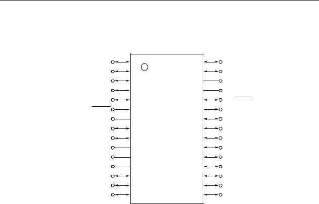
1.4Pin Configuration (Top View)
•30-pin plastic SSOP (7.62 mm (300))
ANI1/P21 |
1 |
30 |
ANI2/P22 |
ANI0/P20 |
2 |
29 |
ANI3/P23 |
P01/TI010/TO00 |
3 |
28 |
AVSS |
P00/TI000 |
4 |
27 |
AVREF |
P120/INTP0/EXLVI |
5 |
26 |
P10/SCK10/TxD0 |
RESET |
6 |
25 |
P11/SI10/RxD0 |
FLMD0 |
7 |
24 |
P12/SO10 |
P122/X2/EXCLK/OCD0BNote |
8 |
23 |
P13/TxD6 |
P121/X1/OCD0ANote |
9 |
22 |
P14/RxD6 |
REGC |
10 |
21 |
P15/TOH0 |
VSS |
11 |
20 |
P16/TOH1/INTP5 |
VDD |
12 |
19 |
P17/TI50/TO50 |
P60/SCL0 |
13 |
18 |
P30/INTP1 |
P61/SDA0 |
14 |
17 |
P31/INTP2/OCD1ANote |
P33/TI51/TO51/INTP4 |
15 |
16 |
P32/INTP3/OCD1BNote |
Note PD78F0503D (product with on-chip debug function) only
Cautions 1. Make AVSS the same potential as VSS.
2.Connect the REGC pin to VSS via a capacitor (0.47 to 1 F: recommended).
3.ANI0/P20 to ANI3/P23 are set in the analog input mode after release of reset.
User’s Manual U17328EJ5V0UD |
19 |

CHAPTER 1 OUTLINE
• 36-pin plastic FLGA (4x4)
Top View |
Bottom View |
6
5
4
3
2
1
A B C D E F F E D C B A
Index mark
Pin No. |
Pin Name |
Pin No. |
|
Pin Name |
Pin No. |
Pin Name |
||
A1 |
NCNote1 |
C1 |
P17/TI50/TO50 |
E1 |
AVREF |
|||
A2 |
P32/INTP3/OCD1BNote2 |
C2 |
P14/RxD6 |
E2 |
AVSS |
|||
A3 |
P30/INTP1 |
C3 |
P13/TxD6 |
E3 |
P22/ANI2 |
|||
A4 |
P61/SDA0 |
C4 |
P00/TI000 |
E4 |
P21/ANI1 |
|||
A5 |
P33/TI51/TO51/INTP4 |
C5 |
VDD |
E5 |
FLMD0 |
|||
A6 |
NCNote1 |
C6 |
P121/X1/OCD0ANote2 |
E6 |
|
|||
RESET |
|
|||||||
B1 |
P31/INTP2/OCD1ANote2 |
D1 |
P11/SI10/RxD0 |
F1 |
NCNote1 |
|||
B2 |
P16/TOH1/INTP5 |
D2 |
P12/SO10 |
F2 |
P23/ANI3 |
|||
|
|
|
|
|
|
|
|
|
B3 |
P15/TOH0 |
D3 |
P10/SCK10/TxD0 |
F3 |
P20/ANI0 |
|||
B4 |
P60/SCL0 |
D4 |
REGC |
F4 |
P01/TI010/TO00 |
|||
B5 |
EVDD |
D5 |
VSS |
F5 |
P120/INTP0/EXLVI |
|||
B6 |
EVSS |
D6 |
P122/X2/EXCLK/ |
F6 |
NCNote1 |
|||
|
|
|
OCD0BNote2 |
|
|
|
||
<R> Notes 1. It is recommended to connect NC to VSS.
2. PD78F0503D (product with on-chip debug function) only
Cautions 1. Make AVSS and EVSS the same potential as VSS.
2.Make EVDD the same potential as VDD.
3.Connect the REGC pin to VSS via a capacitor (0.47 to 1 F: recommended).
4.ANI0/P20 to ANI3/P23 are set in the analog input mode after release of reset.
20 |
User’s Manual U17328EJ5V0UD |
CHAPTER 1 OUTLINE
Pin Identification |
|
|
|
|
||
ANI0 to ANI3: |
Analog input |
P60, P61: |
Port 6 |
|||
AVREF: |
|
Analog reference voltage |
P120 to P122: |
Port 12 |
||
AVSS: |
|
Analog ground |
REGC |
Regulator capacitance |
||
EVDD Note 1: |
|
|
|
|
|
|
|
Power supply for port |
RESET: |
Reset |
|||
EVSS Note 1: |
|
Ground for port |
RxD0, RxD6: |
Receive data |
||
EXCLK: |
|
External clock input |
|
Serial clock input/output |
||
|
SCK10: |
|
||||
|
|
(main system clock) |
SCL0: |
Serial clock input/output |
||
EXLVI: |
|
External potential input |
SDA0: |
Serial data input/output |
||
|
|
for low-voltage detector |
SI10: |
Serial data input |
||
FLMD0: |
|
Flash programming mode |
SO10: |
Serial data output |
||
INTP0 to INTP5: External interrupt input |
TI000, TI010, |
|
||||
NC Notes1, 2: |
|
Non-connection |
TI50, TI51: |
Timer input |
||
OCD0A Note 3, |
|
TO00, |
|
|||
OCD0B Note 3, |
|
TO50, TO51, |
|
|||
OCD1A Note 3, |
|
TOH0, TOH1: |
Timer output |
|||
OCD1B Note 3: |
On chip debug input/output |
TxD0, TxD6: |
Transmit data |
|||
P00, P01: |
|
Port 0 |
VDD: |
Power supply |
||
P10 to P17: |
Port 1 |
VSS: |
Ground |
|||
P20 to P23: |
Port 2 |
X1, X2: |
Crystal oscillator (main system clock) |
|||
P30 to P33: |
Port 3 |
|
|
|
|
|
Notes |
1. |
36-pin plastic FLGA (FC-AA3 type) only |
|
|||
<R> |
2. |
It is recommended to connect NC to VSS. |
|
|||
|
3. |
PD78F0503D (product with on-chip debug function) only |
|
|||
User’s Manual U17328EJ5V0UD |
21 |

CHAPTER 1 OUTLINE
1.5 78K0/Kx2 Microcontroller Lineup
ROM |
RAM |
78K0/KB2 |
78K0/KC2 |
78K0/KD2 |
78K0/KE2 |
78K0/KF2 |
||
|
|
|
|
|
|
|
|
|
|
|
30/36 Pins |
38/44 Pins |
|
48 Pins |
52 Pins |
64 Pins |
80 Pins |
|
|
|
|
|
|
|
|
|
128 KB |
7 KB |
− |
− |
|
− |
PD78F0527DNote |
PD78F0537DNote |
PD78F0547DNote |
|
|
|
|
|
|
PD78F0527 |
PD78F0537 |
PD78F0547 |
|
|
|
|
|
|
|
|
|
96 KB |
5 KB |
− |
− |
|
− |
PD78F0526 |
PD78F0536 |
PD78F0546 |
|
|
|
|
|
|
|
|
|
60 KB |
3 KB |
− |
− |
|
PD78F0515DNote |
PD78F0525 |
PD78F0535 |
PD78F0545 |
|
|
|
|
|
|
|
|
|
|
|
|
|
|
PD78F0515 |
|
|
|
|
|
|
|
|
|
|
|
|
48 KB |
2 KB |
− |
− |
|
PD78F0514 |
PD78F0524 |
PD78F0534 |
PD78F0544 |
|
|
|
|
|
|
|
|
|
32 KB |
1 KB |
PD78F0503DNote |
PD78F0513DNote |
|
PD78F0513 |
PD78F0523 |
PD78F0533 |
− |
|
|
|
|
|
|
|
|
|
|
|
PD78F0503 |
PD78F0513 |
|
|
|
|
|
|
|
|
|
|
|
|
|
|
24 KB |
1 KB |
PD78F0502 |
PD78F0512 |
PD78F0522 |
PD78F0532 |
− |
||
|
|
|
|
|
|
|
||
16 KB |
768 B |
PD78F0501 |
PD78F0511 |
PD78F0521 |
PD78F0531 |
− |
||
|
|
|
|
|
|
|
|
|
8 KB |
512 B |
PD78F0500 |
|
− |
− |
− |
− |
|
|
|
|
|
|
|
|
|
|
Note Product with on-chip debug function
22 |
User’s Manual U17328EJ5V0UD |

<R>
<R>
<R>
<R>
<R>
CHAPTER 1 OUTLINE
The list of functions of the 78K0/Kx2 microcontrollers is shown below.
|
|
|
|
|
|
|
|
|
|
|
|
(1/2) |
Part Number |
|
78K0/KB2 |
|
|
|
|
78K0/KC2 |
|
|
|
||
Item |
|
30/36 Pins |
|
|
38/44 Pins |
|
|
|
48 Pins |
|
|
|
Flash memory (KB) |
8 |
16 |
24 |
32 |
16 |
24 |
32 |
16 |
24 |
32 |
48 |
60 |
RAM (KB) |
0.5 |
0.75 |
1 |
1 |
0.75 |
1 |
1 |
0.75 |
1 |
1 |
2 |
3 |
Bank (flash memory) |
|
|
− |
|
|
||||||
Power supply voltage |
• Standard products, (A) grade products: VDD = 1.8 to 5.5 V |
||||||||||
|
|
|
|
|
|
• (A2) grade products: VDD = 2.7 to 5.5 V |
|||||
Regulator |
|
|
Provided |
|
|
||||||
|
|
|
|
|
|
|
|
||||
Minimum instruction |
0.1 s (20 MHz: VDD = 4.0 to 5.5 V)/0.2 s (10 MHz: VDD = 2.7 to 5.5 V)/ |
||||||||||
execution time |
|
|
0.4 s (5 MHz: VDD = 1.8 to 5.5 V) |
|
|
||||||
|
|
|
|
|
|
|
|
|
|||
|
Main |
|
High-speed system |
20 MHz: VDD = 4.0 to 5.5 V/10 MHz: VDD = 2.7 to 5.5 V/5 MHz: VDD = 1.8 to 5.5 V |
|||||||
|
|
|
|
|
|
|
|
|
|
||
Clock |
|
Internal high-speed |
− |
|
8 MHz (TYP.): VDD = 1.8 to 5.5 V |
|
|
||||
|
|
|
|
|
|||||||
Subsystem |
|
32.768 kHz (TYP.): VDD = 1.8 to 5.5 V |
|||||||||
|
|
|
oscillation |
|
|
|
|
|
|
||
|
|
|
|
|
|
|
|
|
|||
|
Internal low-speed |
|
240 kHz (TYP.): VDD = 1.8 to 5.5 V |
|
|
||||||
|
oscillation |
|
|
|
|
|
|
||||
|
|
|
|
|
|
|
|
|
|||
|
Total |
23 |
|
31 (38 Pins)/ |
|
41 |
|
||||
Port |
|
|
|
|
|
|
37 (44 Pins) |
|
|
|
|
|
|
|
|
|
|
|
|
|
|
||
N-ch O.D. (6 V |
2 |
|
4 |
|
4 |
|
|||||
|
|
|
|
||||||||
|
tolerance) |
|
|
|
|
|
|
||||
|
|
|
|
|
|
|
|
|
|||
|
16 bits (TM0) |
|
|
1 ch |
|
|
|||||
|
|
|
|
|
|
|
|
|
|||
Timer |
8 bits (TM5) |
|
|
2 ch |
|
|
|||||
|
|
|
|
|
|
|
|
|
|
||
8 bits (TMH) |
|
|
2 ch |
|
|
||||||
|
|
|
|
|
|||||||
|
|
|
|
|
|
|
|
|
|||
|
Watch |
− |
|
|
1 ch |
|
|
||||
|
WDT |
|
|
1 ch |
|
|
|||||
|
|
|
|
|
|
|
|
|
|||
|
3-wire CSI |
|
|
− |
|
|
|||||
interface |
Automatic transmit/ |
|
|
− |
|
|
|||||
UART/3-wire CSINote |
|
|
1 ch |
|
|
||||||
|
receive 3-wire CSI |
|
|
|
|
|
|
||||
Serial |
|
|
|
|
|
|
|
|
|
|
|
UART supporting LIN- |
|
|
1 ch |
|
|
||||||
|
|
|
|
|
|||||||
|
bus |
|
|
|
|
|
|
|
|
||
|
|
|
|
|
|
|
|
|
|||
|
I2C bus |
|
|
1 ch |
|
|
|||||
|
|
|
|
|
|
|
|
|
|||
10-bit A/D |
4 ch |
|
6 ch (38 Pins)/ |
|
8 ch |
||||||
|
|
|
|
|
|
|
8 ch (44 Pins) |
|
|
|
|
|
|
|
|
|
|
|
|
|
|
|
|
Interrupt |
External |
6 |
|
7 |
|
8 |
|
||||
|
|
|
|
||||||||
|
|
|
|
|
|
|
|
|
|||
|
Internal |
14 |
|
16 |
|
|
|||||
|
|
|
|
|
|
|
|
|
|||
Key interrupt |
− |
|
2 ch (38 Pins)/ |
|
4 ch |
||||||
|
|
|
|
|
|
|
4 ch (44 Pins) |
|
|
|
|
|
|
|
|
|
|
|
|
|
|||
|
|
|
|
|
|
|
|
||||
|
RESET pin |
|
|
Provided |
|
|
|||||
Reset |
|
|
|
|
|
|
|
|
|
|
|
POC |
1.59 V ±0.15 V (rise time to 1.8 V: 3.6 ms (MAX.)) |
||||||||||
|
|||||||||||
|
|
|
|
|
|
||||||
|
LVI |
|
|
The detection level of the supply voltage is selectable in 16 steps. |
|||||||
|
|
|
|
|
|
|
|
||||
|
WDT |
|
|
Provided |
|
|
|||||
|
|
|
|
|
|
|
|
|
|||
Clock output/buzzer output |
− |
|
|
|
Clock output only |
||||||
Multiplier/divider |
|
|
− |
|
Provided |
||||||
On-chip debug function |
PD78F0503D only |
|
PD78F0513D only |
|
PD78F0515D only |
||||||
|
|
|
|
|
|
||||||
Operating ambient |
• Standard products, (A) grade products: TA = –40 to +85°C |
||||||||||
temperature |
• (A2) grade products: TA = –40 to +110°C, TA = –40 to +125°C |
||||||||||
Note Select either of the functions of these alternate-function pins.
User’s Manual U17328EJ5V0UD |
23 |

CHAPTER 1 OUTLINE
|
|
|
|
|
|
|
|
|
|
|
|
|
|
|
|
|
|
(2/2) |
Part Number |
|
|
78K0/KD2 |
|
|
|
|
78K0/KE2 |
|
|
|
78K0/KF2 |
|
|||||
Item |
|
|
|
52 Pins |
|
|
|
|
|
64 Pins |
|
|
|
|
80 Pins |
|
||
Flash memory (KB) |
16 |
24 |
32 |
48 |
60 |
96 |
128 |
16 |
24 |
32 |
48 |
60 |
96 |
128 |
48 |
60 |
96 |
128 |
RAM (KB) |
0.75 |
1 |
1 |
2 |
3 |
5 |
7 |
0.75 |
1 |
1 |
2 |
3 |
5 |
7 |
2 |
3 |
5 |
7 |
Bank (flash memory) |
|
|
− |
|
|
4 |
6 |
|
|
− |
|
|
4 |
6 |
|
− |
4 |
6 |
Power supply voltage |
|
|
|
|
• Standard products, (A) grade products: VDD = 1.8 to 5.5 |
V |
|
|
|
|||||||||
<R> |
|
|
|
|
|
• (A2) grade products: VDD = 2.7 to 5.5 V |
|
|
|
|
|
|||||||
Regulator |
|
|
|
|
|
|
|
|
Provided |
|
|
|
|
|
|
|
|
|
|
Minimum instruction |
|
0.1 s (20 MHz: VDD = 4.0 to 5.5 V)/0.2 s (10 MHz: VDD = 2.7 to 5.5 V)/ |
|||||||||||
|
execution time |
|
|
0.4 s (5 MHz: VDD = 1.8 to 5.5 V) |
|
|
||||||||
|
|
|
|
|
|
|
|
|
|
|
|
|
||
|
|
|
Main |
|
High-speed system |
|
20 MHz: VDD = 4.0 to 5.5 V/10 MHz: VDD = 2.7 to 5.5 V/5 MHz: VDD = 1.8 to 5.5 V |
|||||||
|
|
|
|
|
|
|
|
|
|
|
|
|
|
|
|
Clock |
|
Internal high-speed |
|
|
8 MHz (TYP.): VDD = 1.8 to 5.5 V |
|
|
||||||
|
|
|
|
|
|
|
|
|||||||
|
|
|
|
oscillation |
|
|
|
|
|
|
|
|
||
|
|
|
|
|
|
|
|
|
|
|
|
|
||
|
|
|
|
|
|
|
|
|
|
|
|
|
||
|
|
|
Subsystem |
|
|
32.768 kHz (TYP.): VDD = 1.8 to 5.5 V |
|
|
||||||
|
|
|
|
|
|
|
|
|
|
|
|
|||
|
|
|
Internal low-speed |
|
|
240 kHz (TYP.): VDD = 1.8 to 5.5 V |
|
|
||||||
|
|
|
oscillation |
|
|
|
|
|
|
|
|
|||
|
|
|
|
|
|
|
|
|
|
|
|
|
||
|
Port |
|
Total |
|
45 |
|
55 |
|
71 |
|||||
|
|
|
|
|
|
|
|
|
|
|
|
|||
|
|
N-ch O.D. (6 V |
|
4 |
|
4 |
|
4 |
||||||
|
|
|
tolerance) |
|
|
|
|
|
|
|
|
|||
|
|
|
|
|
|
|
|
|
|
|
|
|
||
|
|
|
16 bits (TM0) |
|
|
1 ch |
|
|
2 ch |
|||||
|
|
|
|
|
|
|
|
|
|
|
|
|
||
|
Timer |
|
8 bits (TM5) |
|
|
|
|
2 ch |
|
|
||||
|
|
|
|
|
|
|
|
|
|
|
|
|
|
|
|
|
8 bits (TMH) |
|
|
|
|
2 ch |
|
|
|||||
|
|
|
|
|
|
|
|
|
||||||
|
|
|
|
|
|
|
|
|
|
|
|
|||
|
|
|
Watch |
|
|
|
|
1 ch |
|
|
||||
|
|
|
|
|
|
|
|
|
|
|
|
|||
|
|
|
WDT |
|
|
|
|
1 ch |
|
|
||||
|
|
|
|
|
|
|
|
|
|
|
|
|
||
|
|
|
3-wire CSI |
|
|
− |
|
|
1 ch |
|||||
|
interface |
|
Automatic transmit/ |
|
|
− |
1 ch |
|
1 ch |
|||||
|
|
UART/3-wire CSINote |
|
|
|
|
|
|
||||||
|
|
|
receive 3-wire CSI |
|
|
|
|
|
|
|
|
|||
|
Serial |
|
|
|
|
|
|
|
|
|
|
|
|
|
|
|
UART supporting LIN- |
|
|
|
|
1 ch |
|
|
|||||
|
|
|
|
|
|
|
|
|
||||||
|
|
|
bus |
|
|
|
|
|
|
|
|
|
|
|
|
|
|
|
|
|
|
|
|
|
|
|
|||
|
|
|
I2C bus |
|
|
|
|
1 ch |
|
|
||||
|
|
|
|
|
|
|
|
|
|
|
|
|
||
|
10-bit A/D |
|
|
|
|
8 ch |
|
|
||||||
|
|
|
|
|
|
|
|
|
|
|
|
|
|
|
|
Interrupt |
|
External |
|
8 |
|
|
|
9 |
|
||||
|
|
|
|
|
|
|
|
|||||||
|
|
|
|
|
|
|
|
|
|
|
||||
|
|
|
Internal |
|
16 |
|
|
19 |
|
20 |
||||
|
|
|
|
|
|
|
|
|
|
|
|
|
||
|
Key interrupt |
|
|
|
|
8 ch |
|
|
||||||
|
|
|
|
|
|
|
|
|
|
|
|
|||
|
|
|
|
|
|
|
|
|
|
|
|
|||
|
|
|
RESET pin |
|
|
|
|
Provided |
|
|
||||
|
Reset |
|
|
|
|
|
|
|
|
|
|
|
|
|
|
|
POC |
|
|
1.59 V ±0.15 V (rise time to 1.8 V: 3.6 ms (MAX.)) |
|||||||||
|
|
|
|
|
||||||||||
|
|
|
|
|
|
|
|
|
||||||
|
|
|
LVI |
|
|
|
|
The detection level of the supply voltage is selectable in 16 steps. |
||||||
|
|
|
|
|
|
|
|
|
|
|
|
|||
|
|
|
WDT |
|
|
|
|
Provided |
|
|
||||
|
|
|
|
|
|
|
|
|
|
|||||
|
Clock output/buzzer output |
|
Clock output only |
|
|
Provided |
||||||||
|
|
|
|
|
|
|
|
|
|
|||||
|
Multiplier/divider |
− |
|
Provided |
|
− |
|
Provided |
||||||
|
On-chip debug function |
|
PD78F0527D only |
|
PD78F0537D only |
|
PD78F0547D only |
|||||||
|
|
|
|
|
|
|
|
|
||||||
|
Operating ambient |
|
|
• Standard products, (A) grade products: TA = –40 to +85°C |
||||||||||
<R> temperature |
|
|
• (A2) grade products: TA = –40 to +110°C, TA = –40 to +125°C |
|||||||||||
Note Select either of the functions of these alternate-function pins.
24 |
User’s Manual U17328EJ5V0UD |
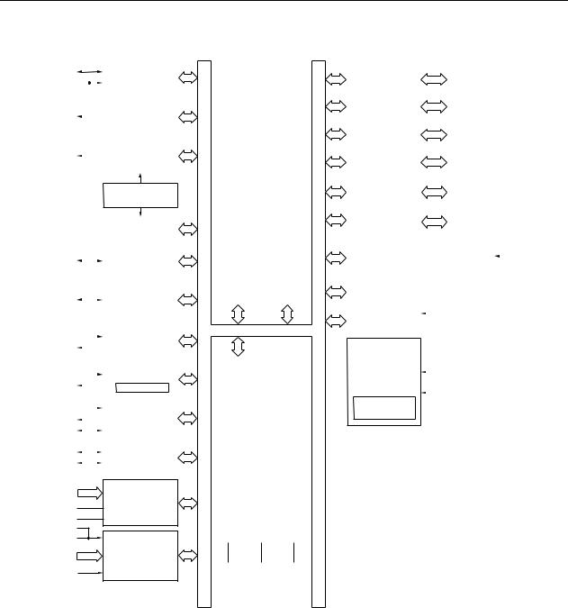
CHAPTER 1 OUTLINE
1.6 Block Diagram
TO00/TI010/P01 |
|
|
|
|
|
16-bit timer/ |
|
|
|
|
|
|
2 |
|
|
|
|
|
|
|
||||||||||
|
|
|
|
|
|
|
|
|
|
Port 0 |
|
|
P00, P01 |
|
||||||||||||||||
|
TI000/P00 |
|
|
|
|
|
|
event counter 00 |
|
|
|
|
|
|
|
|
||||||||||||||
RxD6/P14 (LINSEL) |
|
|
|
|
|
|
|
|
|
|
|
|
Port 1 |
8 |
|
|
P10 to P17 |
|
||||||||||||
|
|
|
|
|
|
|
|
|
|
|
|
|
|
|
|
|
|
|
|
|
|
|
|
|||||||
|
|
|
|
|
|
|
|
|
|
|
|
|
|
|
|
|
|
|
|
|
|
|
|
|||||||
|
TOH0/P15 |
|
|
|
|
|
8-bit timer H0 |
|
|
|
|
|
|
|
|
|
|
|
|
|
|
|
||||||||
|
|
|
|
|
|
|
|
|
|
|
|
|
|
|
|
|
|
|
|
|||||||||||
|
|
|
|
|
|
|
|
|
|
|
|
|
|
|
||||||||||||||||
|
TOH1/P16 |
|
|
|
|
|
|
|
|
|
|
|
|
Port 2 |
4 |
|
|
P20 to P23 |
|
|||||||||||
|
|
|
|
|
|
|
|
|
|
|
|
|
|
|
|
|||||||||||||||
|
|
|
|
|
|
8-bit timer H1 |
|
|
|
|
|
|
4 |
|
|
|
|
|
|
|
||||||||||
|
|
|
|
|
|
|
|
|
|
|
|
|
|
|
|
|
|
|
||||||||||||
|
|
|
|
|
|
|
|
|
|
|
Port 3 |
|
|
P30 to P33 |
|
|||||||||||||||
|
|
|
|
|
|
|
|
|
|
|
|
|
||||||||||||||||||
|
|
|
|
|
|
|
|
|
|
|
|
|
|
|
|
|
|
|
|
|
|
|
|
|||||||
|
|
|
|
|
|
|
|
|
|
|
|
|
|
|
|
|
|
|
|
|
|
|
|
|
|
|
|
|
|
|
|
|
|
|
|
|
|
|
|
|
|
|
|
|
Internal |
low-speed |
|
|
|
|
|
|
2 |
|
|
|
|
|
|
|
|
|
|
|
|
|
|
|
|
|
|
|
|
|
|
|
|
|
|
|
Port 6 |
|
|
P60, P61 |
|
|||||||
|
|
|
|
|
|
|
|
|
|
|
|
|
|
oscillator |
|
|
|
|
|
|
|
|
|
|
|
|
|
|
|
|
|
|
|
|
|
|
|
|
|
|
|
|
|
|
|
|
|
|
|
|
|
|
|
|
|
|
|
|
|
|
|
|
|
|
|
|
|
|
|
|
|
|
|
|
|
|
|
|
|
|
|
|
Port 12 |
3 |
|
|
P120 to P122 |
|
||||
|
|
|
|
|
|
|
|
|
|
|
|
|
|
Watchdog timer |
|
|
|
|
|
|
|
|
||||||||
|
|
|
|
|
|
|
|
|
|
|
|
|
|
|
|
|
|
|
|
|
|
|
|
|
|
|
|
|
||
|
|
|
|
|
|
|
|
|
|
|
|
|
|
|
|
|
|
|
|
|
|
|
|
|
|
|
|
|
|
|
|
|
|
|
|
|
|
|
|
|
|
|
|
|
8-bit timer/ |
|
|
|
|
|
Power on clear/ |
|
|
POC/LVI |
|
|
EXLVI/P120 |
||||
TI50/TO50/P17 |
|
|
|
|
|
|
|
|
|
|
|
low voltage |
|
|
control |
|
|
|||||||||||||
|
|
|
|
|
|
event counter 50 |
|
78K/0 |
|
Flash |
|
indicator |
|
|
|
|
|
|||||||||||||
|
|
|
|
|
|
|
|
|
|
|
|
|
|
|
|
|
|
|
|
|
|
|
|
|
|
|||||
|
|
|
|
|
|
|
|
|
|
|
|
|
|
|
|
|
|
|
|
|
|
|
|
|
|
|
|
|
||
|
|
|
|
|
|
|
|
|
|
|
|
|
|
|
|
|
CPU |
|
|
|
|
|
|
|
|
|
|
|
|
|
|
|
|
|
|
|
|
|
|
|
|
|
|
|
|
|
|
|
memory |
|
|
|
|
|
|
|
|
|
|
|
|
|
|
|
|
|
|
|
|
|
|
|
|
|
|
8-bit timer/ |
|
core |
|
|
|
Reset control |
|
|
|
|
|
|
|
|
|
|
TI51/TO51/P33 |
|
|
|
|
|
|
|
|
|
|
|
|
|
|
|
|
|
|
|
|
|
|||||||||
|
|
|
|
|
|
|
|
|
|
|
|
|
|
|
|
|
|
|
|
|
|
|||||||||
|
|
|
|
|
|
event counter 51 |
|
|
|
|
|
|
|
|
|
|
OCD0ANote 1/X1, OCD1ANote 1/P31 |
|||||||||||||
|
|
|
|
|
|
|
|
|
|
|
|
|
|
|
|
|
|
|
|
|
|
|
|
|||||||
|
|
|
|
|
|
|
|
|
|
|
|
|
|
|
|
|
|
|
|
|
|
|
|
|||||||
|
|
|
|
|
|
|
|
|
|
|
|
|
|
|
|
|
|
|
|
|
On-chip debug Note 1 |
|
|
|
|
|||||
|
|
|
|
|
|
|
|
|
|
|
|
|
|
|
|
|
|
|
|
|
|
|
|
|
||||||
|
|
|
|
|
|
|
|
|
|
|
|
|
|
|
|
|
|
|
|
|
|
|
|
|
OCD0BNote 1/X2, OCD1BNote 1/P32 |
|||||
|
RxD0/P11 |
|
|
|
|
|
|
|
|
|
|
|
Serial |
|
|
|
|
|
|
|
|
|
|
|
|
|
|
|
||
|
|
|
|
|
|
|
|
|
|
|
|
|
|
|
|
|
|
|
|
|
|
|
|
|
||||||
|
TxD0/P10 |
|
|
|
|
|
interface UART0 |
|
|
|
|
|
System |
|
|
|
|
|
|
|
|
|
||||||||
|
|
|
|
|
|
|
|
|
|
|
|
|
|
|
|
|
|
|
||||||||||||
|
|
|
|
|
|
|
|
|
|
|
|
|
|
|
|
|
|
|
|
|
|
|
|
|
|
|
|
|
|
|
|
|
|
|
|
|
|
|
|
|
|
|
|
|
|
|
|
|
|
|
|
|
|
|
|
|
|
|
|
|
|
|
|
|
|
|
|
|
|
|
|
|
|
|
|
Serial |
|
|
|
|
|
control |
|
|
|
|
|
|
|
|
|
|
|
RxD6/P14 |
|
|
|
|
|
|
Internal |
|
|
|
|
|
|
RESET |
|
||||||||||||||
|
|
|
|
|
|
|
|
|
|
interface UART6 |
|
|
|
|
|
|
|
|
|
|||||||||||
|
|
|
|
|
|
|
|
|
|
|
|
|
|
|
|
|
|
|||||||||||||
|
TxD6/P13 |
|
|
|
|
|
|
high-speed |
|
|
|
|
|
|
|
X1/P121 |
|
|||||||||||||
|
|
|
|
|
|
LINSEL |
|
|
|
|
|
|
|
|
|
|||||||||||||||
|
|
|
|
|
|
|
|
|
|
|
|
|
|
|||||||||||||||||
|
|
|
|
|
|
|
|
|
|
|
|
|
|
|
RAM |
|
|
|
|
|
|
|
X2/EXCLK/P122 |
|
||||||
|
SI10/P11 |
|
|
|
|
|
|
|
|
|
|
|
|
|
|
|
Internal high-speed |
|
|
|
|
|||||||||
|
|
|
|
|
|
|
|
|
|
|
|
|
|
|
|
|
|
|
|
|
|
|
|
|
|
|||||
|
|
|
|
|
|
|
|
|
|
|
|
|
|
|
|
|
|
|
|
|
|
|
|
|
|
|||||
|
|
|
|
|
|
|
|
Serial |
|
|
|
|
|
oscillator |
|
|
|
|
|
|
|
|
|
|||||||
|
SO10/P12 |
|
|
|
|
|
|
|
|
|
|
|
|
|
|
|
|
|
|
|
||||||||||
|
|
|
|
|
|
|
|
|
|
|
|
|
|
|
|
|
|
|
|
|
||||||||||
|
|
|
|
|
|
interface CSI10 |
|
|
|
|
|
|
|
|
|
|
|
|
|
|
|
|||||||||
|
|
|
|
|
|
|
|
|
|
|
|
|
|
|
|
|
|
|
|
|
|
|
|
|
|
|
|
|
||
SCK10/P10 |
|
|
|
|
|
|
|
|
|
|
|
|
|
|
|
|
|
|
|
|
|
|
|
|||||||
|
|
|
|
|
|
|
|
|
|
|
|
|
|
|
|
|
|
|
|
|
|
|
||||||||
|
SDA0/P61 |
|
|
|
|
|
|
|
|
|
|
|
|
Voltage regulator |
|
|
|
REGC |
|
|||||||||||
|
|
|
|
|
|
Serial |
|
|
|
|
|
|
|
|
|
|
|
|
|
|
|
|||||||||
|
|
|
|
|
|
|
|
|
|
|
|
|
|
|
|
|
|
|
|
|||||||||||
|
|
|
|
|
|
|
|
|
|
|
|
|
|
|
|
|
|
|
|
|
||||||||||
|
SCL0/P60 |
|
|
|
|
|
interface IIC0 |
|
|
|
|
|
|
|
|
|
|
|
|
|
|
|
||||||||
|
|
|
|
|
|
|
|
|
|
|
|
|
|
|
|
|
|
|||||||||||||
|
|
|
|
|
|
|
|
|
|
|
|
|
|
|
|
|
|
|
|
|
|
|
|
|
|
|
|
|
|
|
ANI0/P20 to
ANI3/P23
AVREF
AVSS
RxD6/P14 (LINSEL)
INTP0/P120
INTP1/P30 to
INTP4/P33
INTP5/P16
4
A/D converter
4Interrupt control
VDD, VSS, FLMD0
EVDDNote 2 EVSSNote 2
Notes 1. Available only in the PD78F0503D (product with on-chip debug function).
2.Available only in the 36-pin plastic FLGA (FC-AA3 type).
User’s Manual U17328EJ5V0UD |
25 |

CHAPTER 1 OUTLINE
<R>
<R>
<R>
1.7 Outline of Functions
|
|
|
|
|
|
|
|
|
|
|
|
|
(1/2) |
|
Item |
|
|
|
PD78F0500 |
|
PD78F0501 |
|
PD78F0502 |
|
PD78F0503 |
PD78F0503D |
|
|
|
|
|
|
|
|
|
|
|
|
|
|
|
Internal |
Flash memory |
8 KB |
|
16 KB |
|
24 KB |
|
32 KB |
|
||||
memory |
(self-programming |
|
|
|
|
|
|
|
|
|
|
|
|
|
supported)Note 1 |
|
|
|
|
|
|
|
|
|
|
|
|
|
|
|
|
|
|
|
|
|
|
|
|
|
|
|
High-speed RAMNote 1 |
512 bytes |
|
768 bytes |
|
1 KB |
|
|
|||||
|
|
|
|
|
|
|
|
|
|
|
|
|
|
Memory space |
|
64 KB |
|
|
|
|
|
|
|
||||
|
|
|
|
|
|
|
|||||||
Main |
High-speed system |
X1 (crystal/ceramic) oscillation, external main system clock input (EXCLK) |
|
||||||||||
system |
|
|
|
|
|
|
|
|
|
|
|
|
|
clock |
Standard |
1 to 20 MHz: VDD = 4.0 to 5.5 V, 1 to 10 MHz: VDD = 2.7 to 5.5 V, |
|
||||||||||
clock |
|
||||||||||||
|
products, |
1 to 5 MHz: VDD = 1.8 to 5.5 V |
|
|
|
|
|
|
|||||
(oscillation |
|
|
|
|
|
|
|
||||||
|
|
|
|
|
|
|
|
||||||
|
(A) grade |
|
|
|
|
|
|
|
|
|
|
|
|
frequency) |
|
|
|
|
|
|
|
|
|
|
|
|
|
|
products |
|
|
|
|
|
|
|
|
|
|
|
|
|
|
|
|
|
|
|
|
|
|
|
|
|
|
|
|
|
|
|
|
|
|||||||
|
|
(A2) grade |
1 to 20 MHz: VDD = 4.0 to 5.5 V, 1 to 10 MHz: VDD = 2.7 to 5.5 V |
|
|||||||||
|
|
products |
|
|
|
|
|
|
|
|
|
|
|
|
|
|
|
|
|
|
|
|
|
|
|
||
|
Internal high-speed |
Internal oscillation |
|
|
|
|
|
|
|
||||
|
oscillation clock |
|
|
|
|
|
|
|
|
|
|
|
|
|
|
|
|
|
|
|
|
|
|
||||
|
|
Standard |
8 MHz (TYP.): VDD = 1.8 to 5.5 V |
|
|
|
|
|
|||||
|
|
products, |
|
|
|
|
|
|
|
|
|
|
|
|
|
(A) grade |
|
|
|
|
|
|
|
|
|
|
|
|
|
products |
|
|
|
|
|
|
|
|
|
|
|
|
|
|
|
|
|
|
|
|
|
||||
|
|
(A2) grade |
8 MHz (TYP.): VDD = 2.7 to 5.5 V |
|
|
|
|
|
|||||
|
|
products |
|
|
|
|
|
|
|
|
|
|
|
|
|
|
|
|
|
|
|
|
|
|
|
||
Internal low-speed oscillation clock |
Internal oscillation |
|
|
|
|
|
|
|
|||||
|
|
|
|
|
|
|
|
|
|
||||
(for TMH1, WDT) |
Standard |
240 kHz (TYP.): VDD = 1.8 to 5.5 V |
|
|
|
|
|
||||||
|
|
products, |
|
|
|
|
|
|
|
|
|
|
|
|
|
(A) grade |
|
|
|
|
|
|
|
|
|
|
|
|
|
products |
|
|
|
|
|
|
|
|
|
|
|
|
|
|
|
|
|
|
|
|
|
||||
|
|
(A2) grade |
240 kHz (TYP.): VDD = 2.7 to 5.5 V |
|
|
|
|
|
|||||
|
|
products |
|
|
|
|
|
|
|
|
|
|
|
|
|
|
|
|
|
|
|
||||||
General-purpose registers |
8 bits × 32 registers (8 bits × 8 registers × 4 banks) |
|
|
||||||||||
Minimum instruction execution time |
0.1 s (high-speed system clock: @ fXH = 20 MHz operation) |
|
|||||||||||
|
|
|
|
|
|
||||||||
|
|
|
0.25 s (internal high-speed oscillation clock: @ fRH = 8 MHz (TYP.) operation) |
||||||||||
|
|
|
|
|
|
|
|
|
|
|
|||
Instruction set |
|
• |
8-bit operation, 16-bit operation |
|
|
|
|
|
|||||
|
|
|
• |
Multiply/divide (8 bits × 8 bits, 16 bits ÷ 8 bits) |
|
|
|||||||
|
|
|
• |
Bit manipulate (set, reset, test, and Boolean operation) |
|
|
|||||||
|
|
|
• |
BCD adjust, etc. |
|
|
|
|
|
|
|
||
|
|
|
|
|
|
|
|
|
|
|
|
||
I/O ports |
|
|
|
Total: |
|
|
23 |
|
|
|
|
||
|
|
|
|
CMOS I/O: |
|
|
21 |
|
|
|
|
||
|
|
|
|
N-ch open-drain I/O (6 V tolerance): |
2 |
|
|
|
|
||||
|
|
|
|
|
|
|
|
||||||
Timers |
|
|
• |
16-bit timer/event counter: |
1 channel |
|
|
||||||
|
|
|
• |
8-bit timer/event counter: |
2 channels |
|
|
||||||
|
|
|
• |
8-bit timer: |
|
2 channels |
|
|
|||||
|
|
|
• |
Watchdog timer: |
1 channel |
|
|
||||||
|
|
|
|
|
|
|
|
||||||
|
Timer outputs |
5 (PWM output: 4, PPG output: 1) |
|
|
|
|
|
||||||
|
|
|
|
|
|
||||||||
A/D converter |
|
|
10-bit resolution × 4 channels (AVREF = 2.3 to 5.5 V)) |
|
|
||||||||
Serial interface |
|
• |
UART supporting LIN-bus: |
1 channel |
|
|
|||||||
|
|
|
• |
3-wire serial I/O/UARTNote 2: |
1 channel |
|
|
||||||
|
|
|
• |
I2C bus: |
|
1 channel |
|
|
|||||
|
|
|
|
|
|
|
|
|
|
|
|
|
|
Notes 1. The internal flash memory capacity, and internal high-speed RAM capacity can be changed using the internal memory size switching register (IMS).
2. Select either of the functions of these alternate-function pins.
26 |
User’s Manual U17328EJ5V0UD |

<R>
<R>
CHAPTER 1 OUTLINE
|
|
|
|
|
|
|
|
|
|
(2/2) |
Item |
|
PD78F0500 |
PD78F0501 |
|
PD78F0502 |
PD78F0503 |
PD78F0503D |
|||
|
|
|
|
|
|
|
|
|
|
|
Vectored |
Internal |
14 |
|
|
|
|
|
|
|
|
interrupt sources |
|
|
|
|
|
|
|
|
|
|
External |
6 |
|
|
|
|
|
|
|
|
|
|
|
|
|
|
|
|
|
|||
|
|
|
|
|
|
|
|
|||
Reset |
|
• Reset using RESET pin |
|
|
|
|||||
|
|
• |
Internal reset by watchdog timer |
|
|
|
||||
|
|
• |
Internal reset by power-on-clear |
|
|
|
||||
|
|
• |
Internal reset by low-voltage detector |
|
|
|
||||
|
|
|
|
|
|
|
|
|
||
On-chip debug function |
None |
|
|
|
|
|
Provided |
|||
|
|
|
|
|
|
|||||
Power supply voltage |
• |
Standard products, (A) grade products: VDD = 1.8 to 5.5 V |
|
|||||||
|
|
• |
(A2) grade products: VDD = 2.7 to 5.5 V |
|
|
|||||
|
|
|
|
|
|
|||||
Operating ambient temperature |
• |
Standard products, (A) grade products: TA = –40 to +85°C |
|
|||||||
|
|
• (A2) grade products: TA = –40 to +110°C, TA = –40 to +125°C |
|
|||||||
|
|
|
|
|
|
|
||||
Package |
|
• 30-pin plastic SSOP (7.62 mm (300) ) |
|
|
||||||
|
|
• |
36-pin plastic FLGA (4×4) |
|
|
|
||||
An outline of the timer is shown below.
|
|
16-Bit Timer/ |
8-Bit Timer/Event Counters |
8-Bit Timers H0 and H1 |
Watchdog |
||
|
|
Event Counter |
50 and 51 |
|
|
Timer |
|
|
|
00 |
|
|
|
|
|
|
|
|
|
|
|
|
|
|
|
TM00 |
TM50 |
TM51 |
TMH0 |
TMH1 |
|
|
|
|
|
|
|
|
|
Function |
Interval timer |
1 channel |
1 channel |
1 channel |
1 channel |
1 channel |
− |
|
External event |
1 channel |
1 channel |
1 channel |
− |
− |
− |
|
counter |
|
|
|
|
|
|
|
|
|
|
|
|
|
|
|
PPG output |
1 output |
− |
− |
− |
− |
− |
|
PWM output |
− |
1 output |
1 output |
1 output |
1 output |
− |
|
Pulse width |
2 inputs |
− |
− |
− |
− |
− |
|
measurement |
|
|
|
|
|
|
|
|
|
|
|
|
|
|
|
Square-wave |
1 output |
1 output |
1 output |
1 output |
1 output |
− |
|
output |
|
|
|
|
|
|
|
|
|
|
|
|
|
|
|
Carrier generator |
− |
− |
− |
− |
1 outputNore |
− |
|
Watchdog timer |
− |
− |
− |
− |
− |
1 channel |
Interrupt source |
2 |
1 |
1 |
1 |
1 |
− |
|
|
|
|
|
|
|
|
|
Note TM51 and TMH1 can be used in combination as a carrier generator mode.
User’s Manual U17328EJ5V0UD |
27 |
CHAPTER 2 PIN FUNCTIONS
2.1 Pin Function List
There are two types of pin I/O buffer power supplies in the 30-pin plastic SSOP (MC-5A4 and MC-CAB types): AVREF, and VDD, and three types of pin I/O buffer power supplies in the 36-pin plastic FLGA (FC-AA3 type): AVREF, EVDD, and VDD. The relationship between these power supplies and the pins is shown below.
Table 2-1. Pin I/O Buffer Power Supplies
Power |
Corresponding Pins |
|
|
|
|
Supply |
30-pin SSOP |
36-pin FLGA |
|
|
|
AVREF |
P20 to P23 |
P20 to P23 |
|
|
|
EVDD |
− |
Port pins other than P20 to P23, |
|
|
P121, and P122 |
|
|
|
VDD |
Pins other than P20 to P23 |
• P121 and P122 |
|
|
• Pins other than port |
|
|
|
(1) Port functions (1/2)
Function Name |
I/O |
Function |
After Reset |
Alternate Function |
||
|
|
|
|
|
|
|
P00 |
I/O |
Port 0. |
Input port |
TI000 |
||
|
|
2-bit I/O port. |
|
|
|
|
P01 |
|
|
TI010/TO00 |
|||
|
Input/output can be specified in 1-bit units. |
|
||||
|
|
|
|
|
|
|
|
|
Use of an on-chip pull-up resistor can be specified by a software |
|
|
|
|
|
|
setting. |
|
|
|
|
|
|
|
|
|
|
|
P10 |
I/O |
Port 1. |
Input port |
|
|
|
|
SCK10/TxD0 |
|||||
|
|
8-bit I/O port. |
|
|
|
|
P11 |
|
|
SI10/RxD0 |
|||
|
Input/output can be specified in 1-bit units. |
|
||||
|
|
|
|
|
|
|
P12 |
|
|
SO10 |
|||
|
Use of an on-chip pull-up resistor can be specified by a software |
|
||||
|
|
|
|
|
|
|
P13 |
|
|
TxD6 |
|||
|
setting. |
|
||||
P14 |
|
|
|
RxD6 |
||
|
|
|
|
|
|
|
P15 |
|
|
|
TOH0 |
||
|
|
|
|
|
|
|
P16 |
|
|
|
TOH1/INTP5 |
||
|
|
|
|
|
|
|
P17 |
|
|
|
TI50/TO50 |
||
|
|
|
|
|
|
|
P20 to P23 |
I/O |
Port 2. |
Analog input |
ANI0 to ANI3 |
||
|
|
4-bit I/O port. |
|
|
|
|
|
|
Input/output can be specified in 1-bit units. |
|
|
|
|
|
|
|
|
|
|
|
P30 |
I/O |
Port 3. |
Input port |
INTP1 |
||
|
|
4-bit I/O port. |
|
|
|
|
P31 |
|
|
INTP2/OCD1ANote |
|||
|
Input/output can be specified in 1-bit units. |
|
||||
|
|
|
|
|
|
|
P32 |
|
Use of an on-chip pull-up resistor can be specified by a software |
|
INTP3/OCD1BNote |
||
|
|
setting. |
|
|
|
|
P33 |
|
|
TI51/TO51/INTP4 |
|||
|
|
|
||||
|
|
|
|
|
|
|
P60 |
I/O |
Port 6. |
Input port |
SCL0 |
||
|
|
2-bit I/O port. |
|
|
|
|
P61 |
|
|
SDA0 |
|||
|
Output is N-ch open-drain output (6 V tolerance). |
|
||||
|
|
|
|
|
|
|
|
|
Input/output can be specified in 1-bit units. |
|
|
|
|
|
|
|
|
|
|
|
Note |
PD78F0503D only |
28 |
User’s Manual U17328EJ5V0UD |

CHAPTER 2 PIN FUNCTIONS
(1) Port functions (2/2)
Function Name |
I/O |
Function |
After Reset |
Alternate Function |
|
|
|
|
|
|
|
P120 |
I/O |
Port 12. |
Input port |
INTP0/EXLVI |
|
|
|
3-bit I/O port. |
|
|
|
P121 |
|
|
X1/OCD0A |
Note |
|
|
Input/output can be specified in 1-bit units. |
|
|
||
|
|
|
|
|
|
P122 |
|
|
X2/EXCLK/OCD0BNote |
||
|
Only for P120, use of an on-chip pull-up resistor can be |
|
|||
|
|
|
|
|
|
|
|
specified by a software setting. |
|
|
|
|
|
|
|
|
|
Note PD78F0503D only
(2) Non-port functions (1/2)
|
|
Function Name |
I/O |
Function |
After Reset |
Alternate Function |
||||
|
|
|
|
|
|
|
|
|
|
|
|
ANI0 to ANI3 |
Input |
A/D converter analog input |
Analog |
P20 to P23 |
|||||
|
|
|
|
|
|
|
input |
|
|
|
|
|
|
|
|
|
|
|
|
|
|
|
EXLVI |
Input |
Potential input for external low-voltage detection |
Input port |
P120/INTP0 |
|||||
|
|
|
|
|
|
|
|
|
|
|
|
FLMD0 |
− |
Flash memory programming mode setting |
− |
|
− |
||||
|
|
|
|
|
|
|
|
|
|
|
|
INTP0 |
Input |
External interrupt request input for which the valid edge (rising |
Input port |
P120/EXLVI |
|||||
|
|
|
|
|
|
edge, falling edge, or both rising and falling edges) can be |
|
|
|
|
|
INTP1 |
|
|
P30 |
||||||
|
|
specified |
|
|||||||
|
|
|
|
|
|
|
|
|
|
|
|
INTP2 |
|
|
P31/OCD1ANote |
||||||
|
|
|
|
|||||||
|
|
|
|
|
|
|
|
|
|
|
|
INTP3 |
|
|
|
P32/OCD1BNote |
|||||
|
|
|
|
|
|
|
|
|
|
|
|
INTP4 |
|
|
|
P33/TI51/TO51 |
|||||
|
|
|
|
|
|
|
|
|
|
|
|
INTP5 |
|
|
|
P16/TOH1 |
|||||
|
|
|
|
|
|
|
|
|
|
|
|
REGC |
− |
Connecting regulator output (2.5 V) stabilization capacitance |
− |
|
− |
||||
|
|
|
|
|
|
for internal operation. |
|
|
|
|
|
|
|
|
|
|
Connect to VSS via a capacitor (0.47 to 1 F: recommended). |
|
|
|
|
|
|
|
|
|
|
|
|
|
|
|
|
|
|
|
|
Input |
System reset input |
− |
|
− |
|
RESET |
||||||||||
|
|
|
|
|
|
|
|
|
|
|
|
RxD0 |
Input |
Serial data input to UART0 |
Input port |
P11/SI10 |
|||||
|
|
|
|
|
|
|
|
|
|
|
|
RxD6 |
Input |
Serial data input to UART6 |
Input port |
P14 |
|||||
|
|
|
|
|
|
|
|
|
|
|
|
TxD0 |
Output |
Serial data output from UART0 |
Input port |
|
|
|
|||
|
P10/SCK10 |
|
||||||||
|
|
|
|
|
|
|
|
|
|
|
|
TxD6 |
Output |
Serial data output from UART6 |
Input port |
P13 |
|||||
|
|
|
|
|
|
|
|
|
|
|
|
|
I/O |
Clock input/output for CSI10 |
Input port |
P10/TxD0 |
|||||
|
SCK10 |
|
||||||||
|
|
|
|
|
|
|
|
|
|
|
|
SCL0 |
I/O |
Clock input/output for I2C |
Input port |
P60 |
|||||
|
|
|
|
|
|
|
|
|
|
|
|
SDA0 |
I/O |
Serial data I/O for I2C |
Input port |
P61 |
|||||
|
|
|
|
|
|
|
|
|
|
|
|
SI10 |
Input |
Serial data input to CSI10 |
Input port |
P11/RxD0 |
|||||
|
|
|
|
|
|
|
|
|
|
|
|
SO10 |
Output |
Serial data output from CSI10 |
Input port |
P12 |
|||||
|
|
|
|
|
|
|
|
|
|
|
|
TI000 |
Input |
External count clock input to 16-bit timer/event counter 00 |
Input port |
P00 |
|||||
|
|
|
|
|
|
Capture trigger input to capture registers (CR000, CR010) of |
|
|
|
|
|
|
|
|
|
|
16-bit timer/event counter 00 |
|
|
|
|
|
|
|
|
|
|
|
|
|
|
|
|
TI010 |
Input |
Capture trigger input to capture register (CR000) of 16-bit |
Input port |
P01/TO00 |
|||||
|
|
|
|
|
|
timer/event counter 00 |
|
|
|
|
|
|
|
|
|
|
|
|
|
|
|
|
TI50 |
Input |
External count clock input to 8-bit timer/event counter 50 |
Input port |
P17/TO50 |
|||||
|
|
|
|
|
|
|
|
|
|
|
|
TI51 |
|
External count clock input to 8-bit timer/event counter 51 |
|
P33/TO51/INTP4 |
|||||
|
|
|
|
|
|
|
|
|
|
|
Note PD78F0503D only
User’s Manual U17328EJ5V0UD |
29 |

CHAPTER 2 PIN FUNCTIONS
(2) Non-port functions (2/2)
Function Name |
I/O |
Function |
After Reset |
Alternate Function |
|
|
|
|
|
|
|
TO00 |
|
Output |
16-bit timer/event counter 00 output |
Input port |
P01/TI010 |
|
|
|
|
|
|
TO50 |
|
Output |
8-bit timer/event counter 50 output |
Input port |
P17/TI50 |
|
|
|
|
|
|
TO51 |
|
|
8-bit timer/event counter 51 output |
|
P33/TI51/INTP4 |
|
|
|
|
|
|
TOH0 |
|
Output |
8-bit timer H0 output |
Input port |
P15 |
|
|
|
|
|
|
TOH1 |
|
|
8-bit timer H1 output |
|
P16/INTP5 |
|
|
|
|
|
|
X1 |
|
− |
Connecting resonator for main system clock |
Input port |
P121/OCD0ANote 1 |
|
|
|
|
|
|
X2 |
|
− |
|
Input port |
P122/EXCLK/OCD0BNote 1 |
|
|
|
|
|
|
EXCLK |
|
Input |
External clock input for main system clock |
Input port |
P122/X2/OCD0BNote 1 |
|
|
|
|
|
|
VDD |
|
− |
For 30-pin SSOP: Positive power supply for pins other than |
− |
− |
|
|
|
P20 to P23 |
|
|
|
|
|
For 36-pin FLGA: Positive power supply for P121, P122, |
|
|
|
|
|
and non-port pins |
|
|
|
|
|
|
|
|
EVDDNote 2 |
− |
Positive power supply for port pins other than P20 to P23, |
− |
− |
|
|
|
|
P121, and P122. |
|
|
|
|
|
Make the same potential as VDD. |
|
|
|
|
|
|
|
|
AVREF |
|
− |
A/D converter reference voltage input and positive power |
− |
− |
|
|
|
supply for P20 to P23 and A/D converter |
|
|
|
|
|
|
|
|
VSS |
|
− |
For 30-pin SSOP: Ground potential for pins other than P20 |
− |
− |
|
|
|
to P23 |
|
|
|
|
|
For 36-pin FLGA: Ground potential for P121, P122, and |
|
|
|
|
|
non-port pins |
|
|
|
|
|
|
|
|
Note 2 |
− |
Ground potential for port pins other than P20 to P23, P121, |
− |
− |
|
EVSS |
|
||||
|
|
|
and P122. |
|
|
|
|
|
Make the same potential as VSS. |
|
|
|
|
|
|
|
|
AVSS |
|
− |
A/D converter ground potential. Make the same potential as |
− |
− |
|
|
|
VSS. |
|
|
|
|
|
|
|
|
OCD0ANote 1 |
Input |
Connection for on-chip debug mode setting pins |
Input port |
P121/X1 |
|
|
|
|
( PD78F0503D only) |
|
|
|
Note 1 |
|
|
|
|
OCD1A |
|
|
|
P31/INTP2 |
|
|
|
|
|
||
|
|
|
|
|
|
OCD0BNote 1 |
− |
|
|
P122/X2/EXCLK |
|
|
|
|
|
|
|
OCD1BNote 1 |
|
|
|
P32/INTP3 |
|
|
|
|
|
|
|
Notes 1. PD78F0503D only
2. 36-pin plastic FLGA (FC-AA3 type) only
30 |
User’s Manual U17328EJ5V0UD |
Loading...