


NEC PS9713-V, PS9713-V-F3, PS9713, PS9713-F3, PS9713-F4 Datasheet

DATA SHEET
PHOTOCOUPLER
PS9713
1 Mbps, OPEN COLLECTOR OUTPUT, FOR GATE DRIVE INTERFACE
INTELLIGENT POWER MODULE
5-PIN SOP PHOTOCOUPLER
DESCRIPTION
The PS9713 is an optically coupled isolator containing a GaAlAs LED on the input side and a photo diode and a
signal processing circuit on the output side on one chip.
FEATURES
• High instantaneous common mode rejection voltage (CMH, CML = ±15 kV/µs MIN.)
• Small package (5-pin SOP)
• High-speed response (t
• Maximum propagation delays (t
• Pulse width distortion ( | t
• Ordering number of taping product: PS9713-F3, F4: 3 500 pcs/reel
• UL approved: File No. E72422 (S)
• VDE0884 approved (Option)
PHL
= 500 ns MAX., t
PLH
− t
PHL
PLH
− t
| = 270 ns TYP.)
PLH
= 750 ns MAX.)
PHL
= 270 ns TYP.)
−NEPOCTM Series−
APPLICATIONS
•IPM Driver
• General purpose inverter
The information in this document is subject to change without notice. Before using this document, please
confirm that this is the latest version.
Not all devices/types available in every country. Please check with local NEC representative for
availability and additional information.
Document No. P13982EJ2V0DS00 (2nd edition)
Date Published May 2000 NS CP(K)
Printed in Japan
©
1998, 2000

PACKAGE DIMENSIONS (in millimeters)
4.0±0.5
2.1±0.2
1.27
+0.10
–0.05
0.15
TOP VIEW
64
5
13
7.0±0.3
4.4
0.5±0.3
1. Anode
3. Cathode
4. GND
O
5. V
6. V
CC
PS9713
0.4
0.1±0.1
FUNCTIONAL DIAGRAM
1
3
LED
+0.10
–0.05
Output
0.25 M
6
5
4
Shield
ON L
OFF
2
H
Data Sheet P13982EJ2V0DS00
ORDERING INFORMATION
PS9713
Part Number Package Packing Style
Safety Standards
Approval
Application Part
PS9713 5-pin SOP Magazine case 100 pcs UL approved PS9713
PS9713-F3 Embossed Tape 3 500 pcs/reel
PS9713-F4
PS9713-V Magazine case 100 pcs VDE0884 approved
PS9713-V-F3 Embossed Tape 3 500 pcs/reel
PS9713-V-F4
For the application of the Safety Standard, following part number should be used.
*1
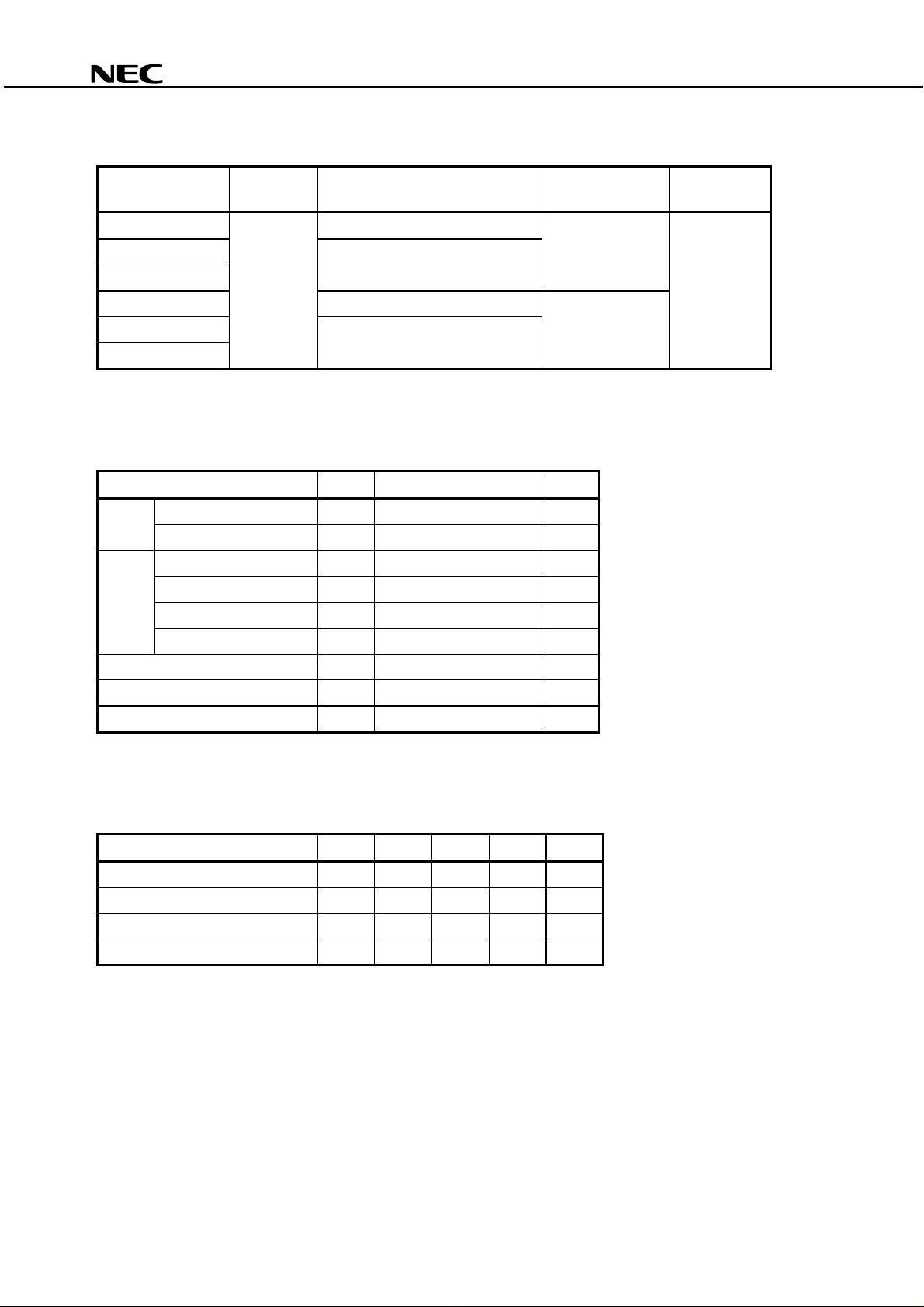
ABSOLUTE MAXIMUM RATINGS (TA = 25 °°°°C, unless otherwise specified)
Parameter Symbol Ratings Unit
Diode Forward Current I
Reverse Voltage V
Detector
Supply Voltage V
Output Voltage V
Output Current I
Power Dissipation P
Isolation Voltage
*1
Operating Ambient Temperature T
Storage Temperature T
F
R
CC
O
O
C
25 mA
3.0 V
−
0.5 to +35 V
−
0.5 to +35 V
15 mA
100 mW
BV 2 500 Vr.m.s .
A
stg
−
40 to +100
−
55 to +125
°
C
°
C
Number
*1
AC voltage for 1 minute at T
*1
A
= 25 °C, RH = 60 % between input and output.
RECOMMENDED OPERATING CONDITIONS
Parameter Symbol MIN. TYP. MAX. Unit
High Level Input Current I
Output Voltage V
Supply Voltage V
LED Off Voltage V
FH
O
CC
F
10 20 mA
030V
4.5 30 V
00.8V
Data Sheet P13982EJ2V0DS00
3

PS9713
ELECTRICAL CHARACTERISTICS (TA = −−−−40 to +100 °°°°C, VCC = 15 V, unless otherwise specified)
*1
Parameter Symbol Conditions MIN.
TYP.
MAX. Unit
Diode Forward Voltage V
Reverse Current I
Terminal Capacitance CtV = 0 V, f = 1 MHz, TA = 25 °C30pF
Detector Low Level Output Voltage V
High Level Output Current I
High Level Supply Current I
Low Level Supply Current I
Coupled
Threshold Input Current
(H → L)
Current Transfer Ratio (IC/IF)CTRIF = 10 mA, VO = 0.6 V 44 110 %
Isolation Resistance R
Isolation Capacitance C
Propagation Delay Time
*2
(H → L)
Propagation Delay Time
*2
(L → H)
Maximum Propagation
PLH
t
Delays
Pulse Width Distorti on
*2
(PWD)
Instantaneous Common
Mode Rejection Voltage
(Output: High)
*3
Instantaneous Common
Mode Rejection Voltage
(Output: Low)
*3
PHL
|t
CM
CM
FIF
= 10 mA 1.3 1.65 2.1 V
R
VR = 3 V 200
OLIF
= 10 mA, VCC = 5 V, IO = 2.4 mA 0.13 0.6 V
OH
VCC = 30 V, VF = 0.8 V 1.0 50
CCH
VCC = 30 V, VF = 0.8 V, VO = open 0.6 1.3 mA
CCL
VCC = 30 V, IF = 10 mA, VO = open 0.6 1.3 mA
FHL
I
VO = 0.8 V, IO = 0.75 mA 1.5 5.0 mA
I-O
V
I-O
I-O
PHL
t
PLH
t
−
t
−
t
= 1 kVDC, RH = 40 to 60 %,
A
T
= 25 °C
V = 0 V, f = 1 MHz, TA = 25 °C0.6pF
IF = 10mA, RL = 20 kΩ, CL = 100 pF,
THHL
V
= 1.5 V, V
PHL
PLH
| 270 650
TA = 25 °C, IF = 0 mA, VO > 3.0 V,
H
CM
V
= 1.5 kV, RL = 20 kΩ,
L
C
= 100 pF
TA = 25 °C, IF = 10 mA, VO < 1.0 V,
L
CM
V
= 1.5 kV, RL = 20 kΩ,
L
C
= 100 pF
THLH
= 2.0 V
11
10
250 500 ns
520 750
−
200 270 650
15 kV/
15 kV/
µ
A
µ
A
Ω
µ
s
µ
s
4
Data Sheet P13982EJ2V0DS00
 Loading...