


NEC PS2801-1, PS2801-1-F3, PS2801-1-F4, PS2801-4, PS2801-4-F3 Datasheet
...
DATA SHEET
©
PHOTOCOUPLER
PS2801-1,PS2801-4
HIGH ISOLATION VOLTAGE
SOP PHOTOCOUPLER
DESCRIPTION
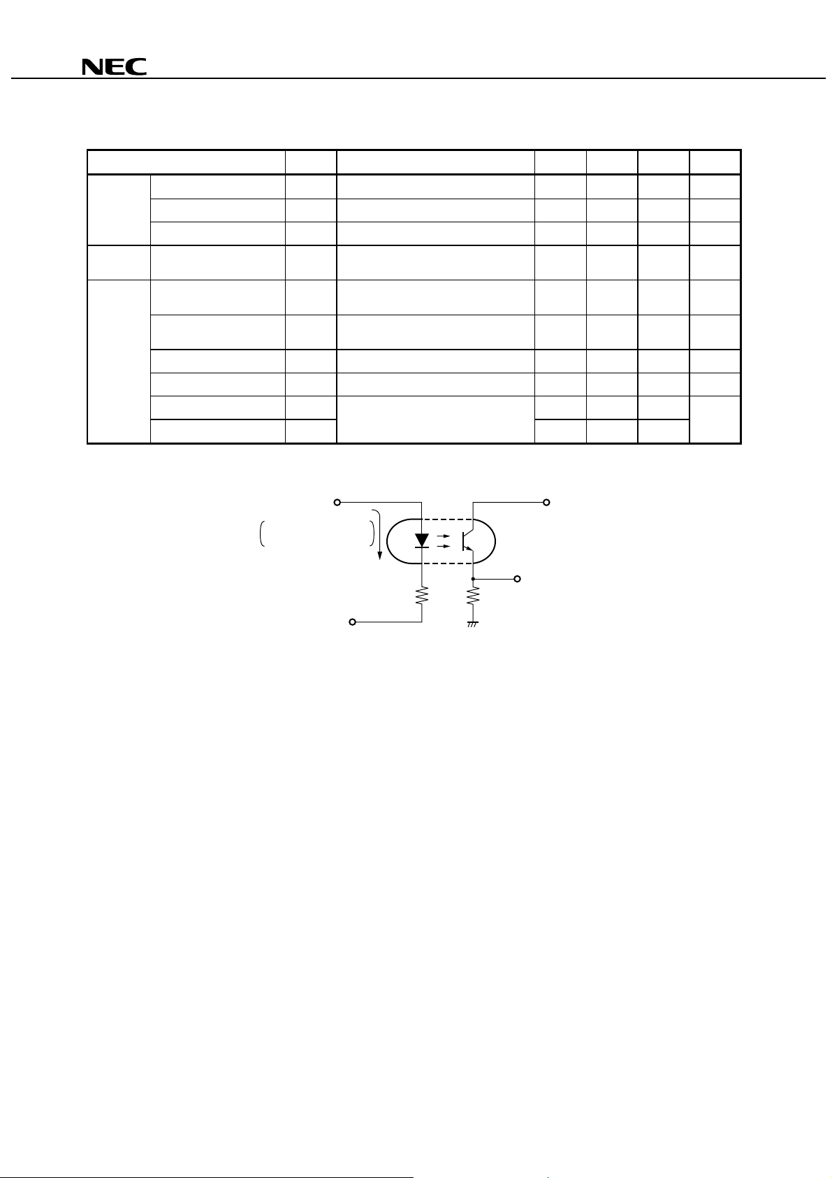
The PS2801-1 and PS2801-4 are optically coupled isolators containing a GaAs light emitting diode and an NPN
silicon phototransistor in a plastic SOP for high density applications.
This package has shield effect to cut off ambient light.
FEATURES
• High isolation voltage (BV = 2 500 Vr.m.s.)
• Small and thin package (4,16-pin SOP, Pin pitch 1.27 mm)
• High collector to emitter voltage (V
• High-speed switching (tr = 3 µs TYP., tf = 5 µs TYP.)
• UL approved: File No. E72422 (S)
• VDE0884 approved (Option): PS2801-4 only
• Operating number of taping product: PS2801-1-F3, F4, PS2801-4-F3, F4
CEO
= 80 V)
NEPOCTM Series
−
−
APPLICATIONS
• Programmable logic controllers
• Measuring instruments
• Power supply
•Hybrid IC
The information in this document is subject to change without notice.
Document No. P12277EJ6V0DS00 (6th edition)
Date Published May 1998 NS CP(K)
Printed in Japan
The mark
••••
shows major revised points.
1991
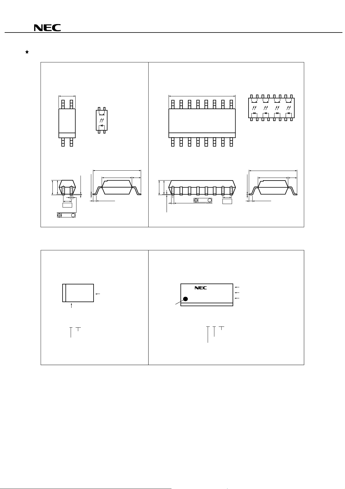
PACKAGE DIMENSIONS (in millimeters)
PS2801-1,PS2801-4
2.0
2.3 MAX.
0.4±0.1
MARKING
2.7±0.3
1.27
0.12
PS2801-1
0.1±0.1
M
–0.05
+0.10
0.15
TOP VIEW
43
12
7.0±0.3
4.4
0.5±0.3
1. Anode
2. Cathode
3. Emitter
4. Collector
1.3
2.0
2.3 MAX.
0.1±0.1
+0.10
–0.05
10.3±0.3
0.12 0.40
PS2801-4
M
1.27
TOP VIEW
161514131211 10 9
12345678
1. 3. 5. 7.
2. 4. 6. 8.
9. 11. 13. 15.
10. 12. 14. 16.
–0.05
+0.10
0.15
0.5±0.3
Anode
Cathode
Emitter
Collector
7.0±0.3
4.4
1.3
PS2801-1
1 503
Last number of type No. : 1
5 03
Weekly Serial Code
Assembly Year
Assembly lot
No. 1 pin
Mark
PS2801-4
JAPAN
PS28012-4
N 503
N 5 03
Weekly Serial Code
Assembly Year
CTR Rank Name
Company & Country Name
Type Number
Assembly lot
2

ABSOLUTE MAXIMUM RATINGS (TA = 25 °C, unless otherwise specified)
Parameter Symbol Ratings Unit
PS2801-1 PS2801-4
PS2801-1,PS2801-4
Diode Forward Current (DC) I
Reverse Voltage V
Power Dissipation Derati ng
Power Dissipation P
Peak Forward Current
*1
Transistor Collector to Emitter Voltage V
Emitter to Collector Voltage V
Collector Current I
Power Dissipation Derati ng
Power Dissipation P
Isolation Voltage
*2
Operating Ambient Temperature T
Storage Temperature T
PW = 100
*1
AC voltage for 1 minute at TA = 25 °C, RH = 60 % between input and output
*2
s, Duty Cycle = 1 %
µ
F
R
∆
PD/°C 0.6 0.8 mW/°C
D
FP
I
CEO
ECO
C
∆
PC/°C1.2mW/
C
50 mA
6V
60 80 mW/ch
1A
80 V
6V
50 mA/ch
120 mW/ch
BV 2 500 Vr.m.s.
A
stg
−
55 to +100
−
55 to +150
°
C
°
C
°
C
3
ELECTRICAL CHARACTERISTICS (TA = 25 °C)
Parameter Symbol Conditions MIN. TYP. MAX. Unit
PS2801-1,PS2801-4
Diode Forward Voltage V
Reverse Current I
Terminal Capacitance C
Transistor
Collector to Emitter
Dark Current
Coupled
Current Transfer Ratio
C/IF
)
(I
Collector Saturation
CTR I
V
Voltage
Isolation Resistance R
Isolation Capacitance C
Rise Time
Fall Time
Test circuit for switching time
*1
*1
*1
Pulse Input
PW = 100 s
Duty Cycle = 1/10
F
IF = 5 mA 1.1 1.4 V
R
VR = 5 V 5
t
V = 0 V, f = 1.0 MHz 30 pF
CEO
I
VCE = 80 V, IF = 0 mA 100 nA
F
= 5 mA, VCE = 5 V 80 600 %
CE(sat)IF
t
t
= 10 mA, IC = 2 mA 0.3 V
I-O
I-O
V
= 1.0 kV
I-O
V = 0 V, f = 1.0 MHz 0.4 pF
r
VCC = 5 V, IC = 2 mA, RL = 100
f
DC
Ω
10
11
3
5
VCC
µ
F
I
VOUT
50 Ω
RL = 100 Ω
µ
A
Ω
µ
s
4
 Loading...