


NEC PS7206-1A, PS7206-1A-E3, PS7206-1A-E4, PS7206-1A-F3, PS7206-1A-F4 Datasheet

DATA SHEET
Solid State Relay
PS7206-1A
4-PIN SOP, 0.6 ΩΩΩΩ LOW ON-STATE RESISTANCE
600 mA CONTINUOUS LOAD CURRENT
1-ch Optical Coupled MOS FET
DESCRIPTION
The PS7206-1A is a low on-state resistance solid state relay containing GaAs LEDs on the light emitting side
(input side) and MOS FETs on the output side.
It is suitable for PLC, etc. because of its large continuous load current and low on-state resistance.
FEATURES
• Low on-state resistance (Ron = 0.6 Ω TYP.)
• Large continuous load current (IL = 600 mA)
• 1 channel type (1 a output)
• Designed for AC/DC switching line changer
• Small and thin package (4-pin SOP, Height = 2.1 mm)
• High isolation voltage (BV = 1 500 Vr.m.s.)
• Low offset voltage
• Ordering number of taping product: PS7206-1A-E3, E4, F3, F4
OCMOS FET
APPLICATIONS
• Measurement equipment
• FA equipment
The information in this document is subject to change without notice. Before using this document, please
confirm that this is the latest version.
Not all devices/types available in every country. Please check with local NEC representative for
availability and additional information.
Document No. P14496EJ5V0DS00 (5th edition)
Date Published June 2000 NS CP(K)
Printed in Japan
The mark
••••
shows major revised points.
©
1999, 2000
PS7206-1A
–0.05
+0.08
2.05
–0.05
+0.08
0.05
0.40
4.0±0.5
2.54
+0.10
–0.05
0.25 M
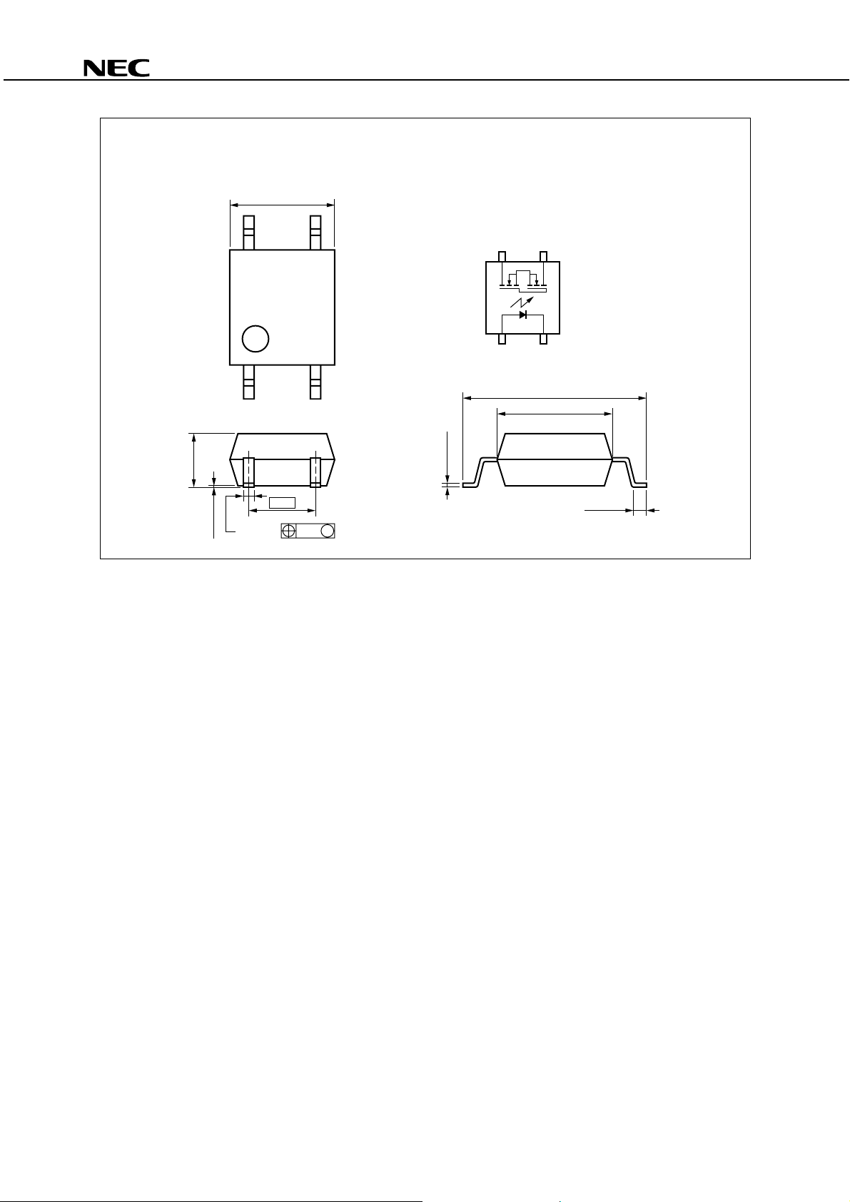
PACKAGE DIMENSIONS
in millimeters
–0.05
+0.10
0.15
TOP VIEW
43
1. LED Anode
2. LED Cathode
3. MOS FET
4. MOS FET
12
7.0±0.3
4.4
0.5±0.3
2
Data Sheet P14496EJ5V0DS00
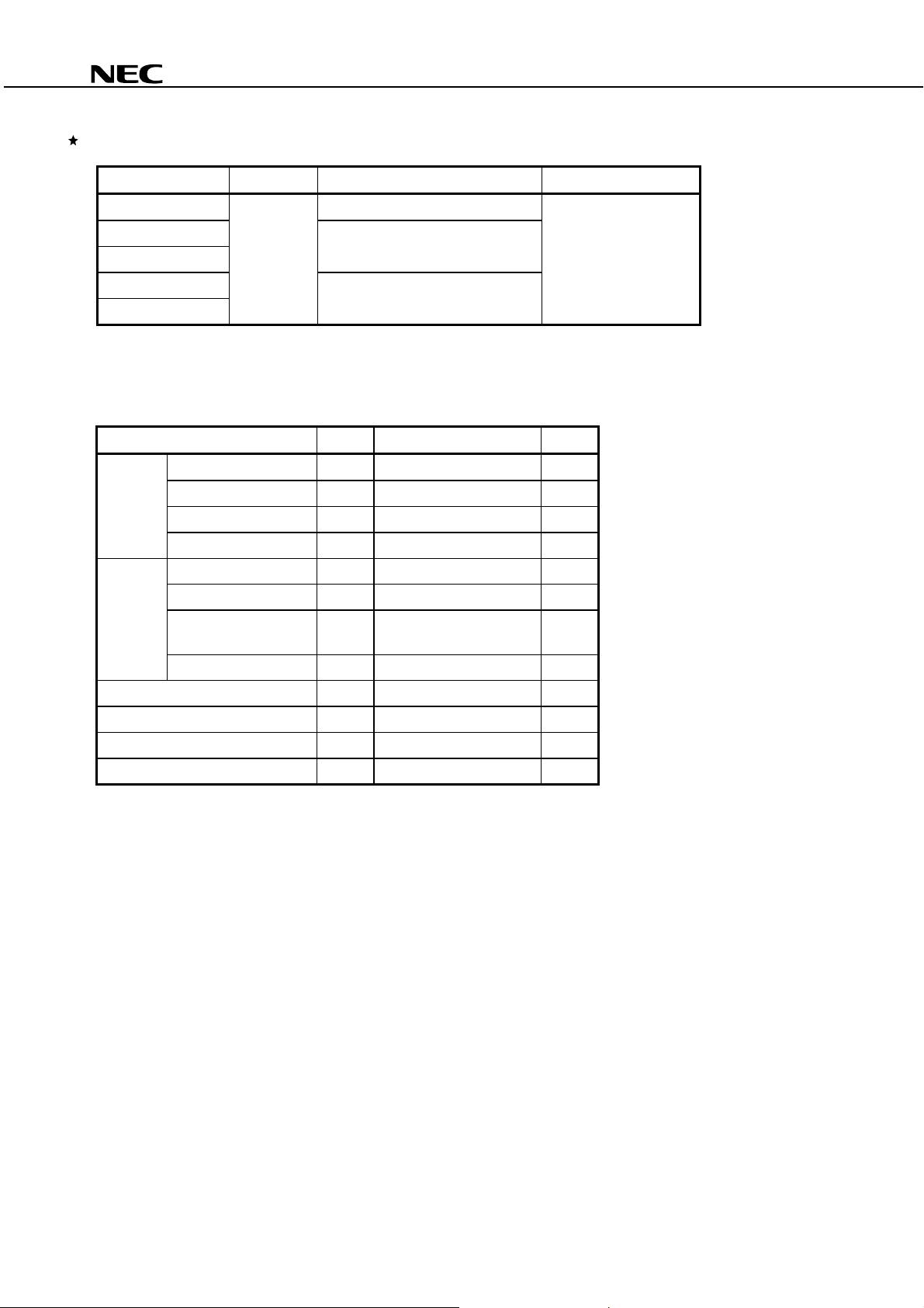
ORDERING INFORMATION
PS7206-1A
Part Number Package Packing Style
Application Part Number
PS7200B-1A 4-pin SOP Magazine case 100 pcs PS7200B-1A
PS7200B-1A-E3 Embossed Tape 900 pcs/reel
PS7200B-1A-E4
PS7200B-1A-F3 Emboss ed Tape 3 500 pcs/reel
PS7200B-1A-F4
For the application of the Safety Standard, following part number should be used.
*1
ABSOLUTE MAXIMUM RATINGS (TA = 25 °°°°C, unless otherwise specified)
Parameter Symbol Ratings Unit
Diode Forward Current (DC) I
Reverse Voltage V
Power Dissipation P
Peak Forward Current
*1
MOS FET Break Down Voltage V
Continuous Load Current I
Pulse Load Current
*2
(AC/DC Connection)
Power Dissipation P
Isolation Voltage
*3
Total Power Dissipat i on P
Operating Ambient Temperature T
Storage Temperature T
F
R
D
FP
I
L
L
LP
I
D
50 mA
5.0 V
50 mW
1A
60 V
600 mA
1.2 A
300 mW
BV 1 500 Vr.m.s.
T
A
stg
350 mW
−
40 to +85
−
40 to +100
°
C
°
C
*1
PW = 100 µs, Duty Cycle = 1 %
*1
PW = 100 ms, 1 shot
*2
AC voltage for 1 minute at TA = 25 °C, RH = 60 % between input and output
*3
Data Sheet P14496EJ5V0DS00
3
RECOMMENDED OPERATING CONDITIONS (TA = 25 °°°°C)
Parameter Symbol MIN. TYP. MAX. Unit
PS7206-1A
LED Operating Current I
LED Off Voltage V
F
F
21020mA
00.5V
ELECTRICAL CHARACTERISTICS (TA = 25 °°°°C)
Parameter Symbol Conditions MIN. TYP. MAX. Unit
Diode Forward Voltage V
Reverse Current I
MOS FET Off-state Leakage Current I
Output Capacitance C
Coupled LED On-s t ate Current I
On-state Resistance R
Turn-on Time t
Turn-off Time t
Isolation Resistance R
Isolation Capacitance C
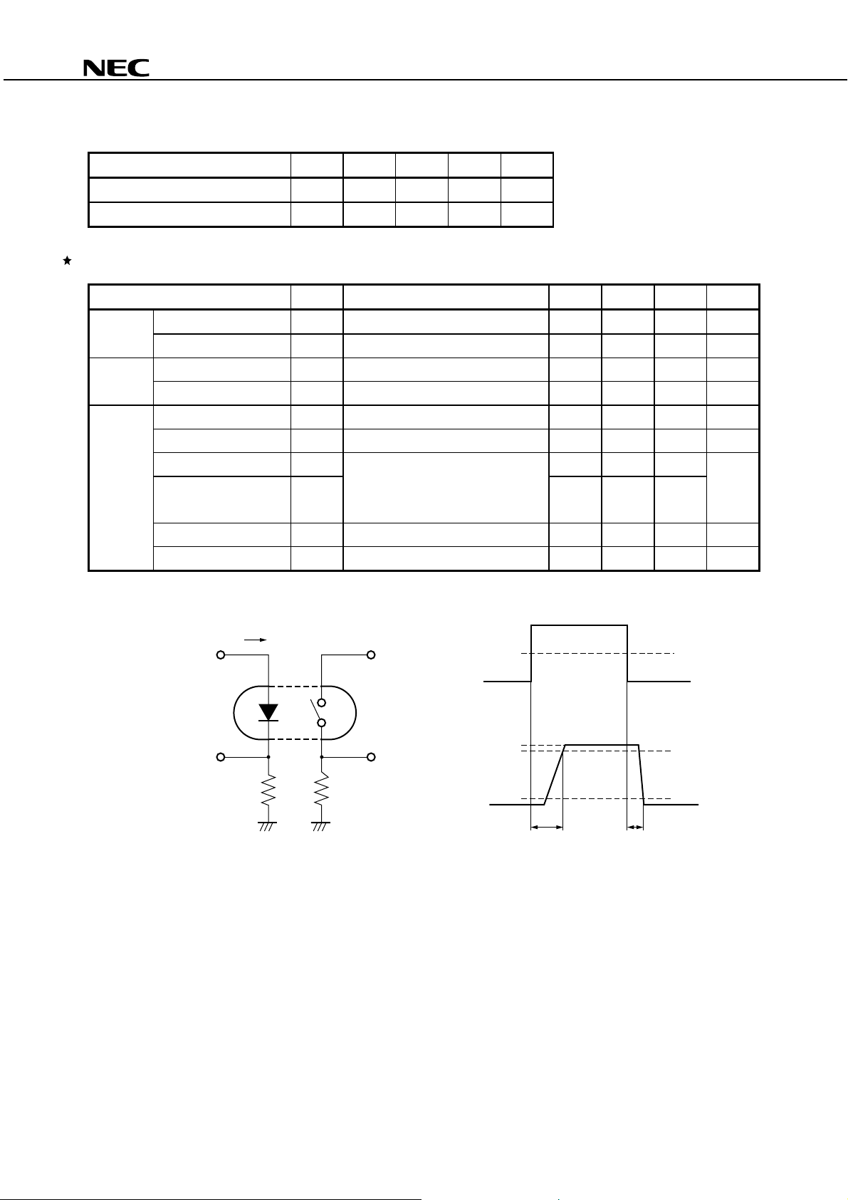
Test Circuit for Switching Time
*1
F
IF = 10 mA 1.2 1.4 V
R
VR = 5 V 5.0
Loff
VD = 60 V 1.0
out
VD = 0 V, f = 1 MHz 70 pF
FonIL
= 600 mA 2.0 mA
onIF
= 10 mA, IL = 600 mA, t ≤ 10 ms 0.6 0.8
on
IF = 10 mA, VO = 5 V, RL = 500 Ω,0.42.0ms
off
PW ≥ 10 ms 0.08 0.5
I-O
I-O
V
= 1.0 kV
I-O
V = 0 V, f = 1 MHz 0.5 pF
µ
A
µ
A
Ω
DC
10
9
Ω
I
F
Pulse Input
Input monitor monitorV
R
in
R
L
V
L
Input
50 %
0
O
VO = 5 V
90 %
Output
10 %
t
on
t
off
4
Data Sheet P14496EJ5V0DS00
 Loading...