


NEC PS9701, PS9701-E3, PS9701-E4, PS9701-F3, PS9701-V Datasheet

DATA SHEET
©
PHOTOCOUPLER
PS9701
HIGH SPEED DIGITAL OUTPUT TYPE
5-PIN SOP PHOTOCOUPLER
NEPOC
−
DESCRIPTION
The PS9701 is an optically coupled isolator containing a GaAlAs LED on light emitting side (input side) and a
photodiode and a signal processing circuit on light receiving side (output side) on one chip.
This is SOP (Small Outline Package) type for high-density applications.
FEATURES
• High isolation voltage (BV = 2 500 Vr.m.s.)
• Small and thin package (5-pin SOP)
• High-speed response (t
• Low threshold input current (I
• Open-collector type
• Ordering number of taping product: PS9701-1-E3, E4, F3, F4
• UL approved: File No. E72422 (S)
• VDE0884 approved (Option)
PHL
= 36 ns TYP., t
FHL
= 2.5 mA TYP.)
PLH
= 60 ns TYP.)
TM
Series
−
APPLICATIONS
• Computer and peripheral manufactures
• Measurement equipment
• Audio-Visual
The information in this document is subject to change without notice. Before using this document, please
confirm that this is the latest version.
Not all devices/types available in every country. Please check with local NEC representative for
availability and additional information.
Document No. P11437EJ4V0DS00 (4th edition)
Date Published September 1999 NS CP(K)
Printed in Japan
The mark
••••
shows major revised points.
1994, 1999
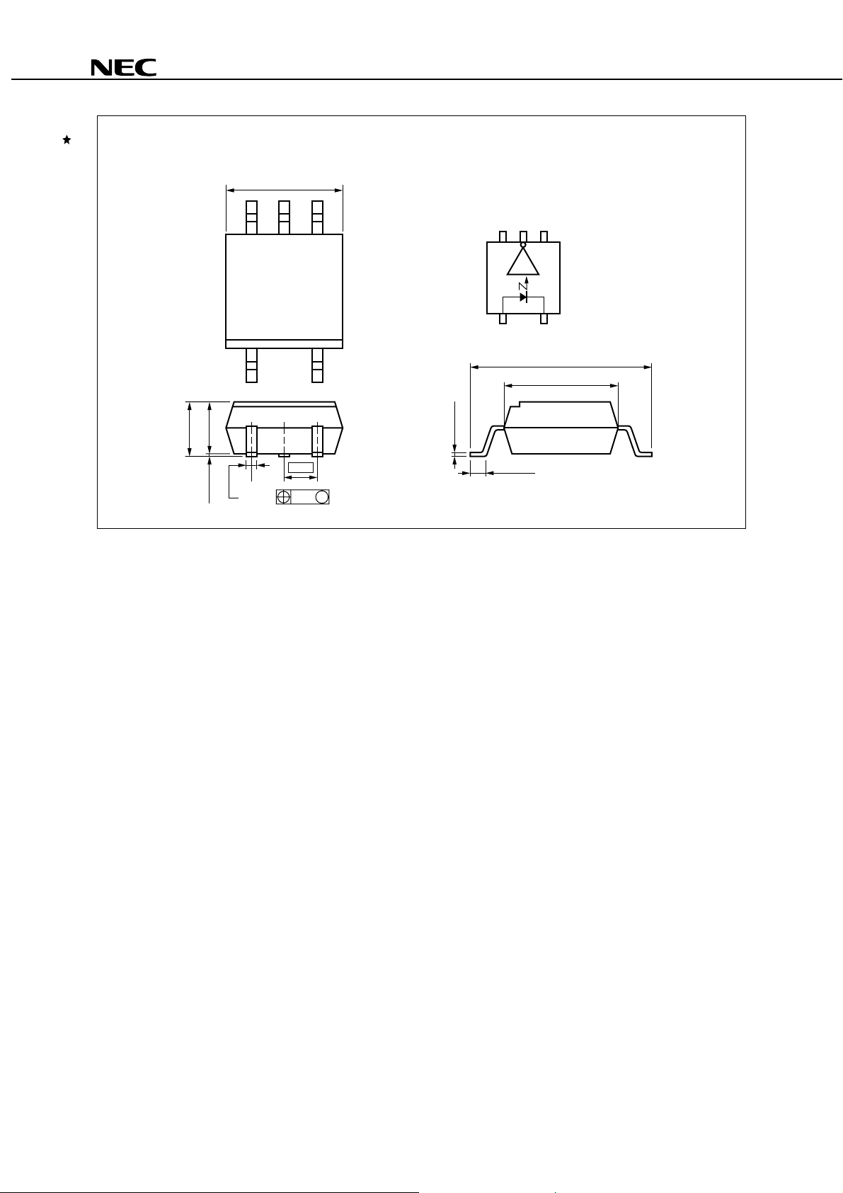
2.00.1±0.1
2.1±0.2
4.0±0.5
1.27
PACKAGE DIMENSIONS
in millimeters
64
13
+0.10
–0.05
0.15
0.5±0.3
TOP VIEW
5
7.0±0.3
4.4
1. Anode
3. Cathode
4. GND
O
5. V
6. V
CC
PS9701
0.4
+0.10
–0.05
0.25 M
2
Data Sheet P11437EJ4V0DS00

ORDERING INFORMATION
PS9701
Part Number Package Packing Style
Safety Standards
Approval
Application Part
PS9701 5-pin SOP Magazine case 100 pcs UL approved PS9701
PS9701-E3 Embossed Tape 900 pcs/reel
PS9701-E4
PS9701-F3 Emboss ed Tape 3 500 pcs/reel
PS9701-F4
PS9701-V Magazine case 100 pcs VDE0884 approved
PS9701-V-E3 Embossed Tape 900 pcs/reel
PS9701-V-E4
PS9701-V-F3 Emboss ed Tape 3 500 pcs/reel
PS9701-V-F4
For the application of the Safety Standard, following part number should be used.
*1
ABSOLUTE MAXIMUM RATINGS (TA = 25 °°°°C, unless otherwise specified)
Parameter Symbol Ratings Unit
Diode Forward Current I
Reverse Voltage V
Detector Supply Voltage V
Output Voltage V
Output Current I
Power Dissipation P
Isolation Voltage
*1
Operating Ambient Temperature T
Storage Temperature T
F
R
CC
O
O
C
30 mA
5V
7V
7V
50 mA
85 mW
BV 2 500 Vr.m.s.
A
stg
–40 to +85
–55 to +125
°
C
°
C
Number
*1
A
AC voltage for 1 minute at T
*1
= 25 °C, RH = 60 % between input and output
RECOMMENDED OPERATING CONDITIONS
Parameter Symbol MIN. TYP. MAX. Unit
Low Level Input Current I
High Level Input Current I
Supply Voltage V
Operating Ambient Temperature T
Remark
By-pass capacitor of more than 0.1
FL
FH
CC
A
0 250
57.515mA
4.5 5.0 5.5 V
02570°C
F is used between VCC and GND near the device.
µ
Data Sheet P11437EJ4V0DS00
µ
A
3

ELECTRICAL CHARACTERISTICS (TA = 0 to +70 °°°°C, unless otherwise specified)
Parameter Symbol Conditions MIN. TYP. MAX. Unit
PS9701
Diode Forward Voltage V
Reverse Current I
Terminal Capacitance CtV = 0 V, f = 1 MHz, TA = 25 °C60pF
Detector High Level Output Current I
Low Level Output Voltage V
High Level Supply Current I
Low Level Supply Current I
Threshold Input Current
(H → L)
Isolation Resistance R
Isolation Capacitance C
Propagation Delay Time
*1
(H → L)
Propagation Delay Time
*1
(L → H)
Rise Time t
Fall Time t
Test circuit for propagation delay time
*1
FIF
= 10 mA, TA = 25 °C 1.4 1.65 1.9 V
R
VR = 5 V, TA = 25 °C10
OH
VCC = VO = 5.5 V, IF = 250 µA 2 250
OL
VCC = 5.5 V, IF = 7.5 mA, IO = 13 mA 0.3 0.6 V
CCH
VCC = 5.5 V, IF = 0 mA 4 6 8 mA
CCL
VCC = 5.5 V, IF = 10 mA 9 12 15 mA
FHL
I
CC
V
= 5 V, VO = 0.8 V, RL = 350
I-O
V
I-O
I-O
PHL
t
PLH
t
r
f
= 1 kVDC, RH = 40 to 60 %,
A
T
= 25 °C
V = 0 V, f = 1 MHz, TA = 25 °C0.6pF
VCC = 5 V, IF = 7.5 mA, RL = 350 Ω,
L
C
= 15 pF, TA = 25 °C
TA = 25 °C 0.5 2.5 5.0Coupled
Ω
11
10
7
36 75 ns
60 75
20
10
µ
µ
mA
Ω
A
A
Pulse Input
(PW = 1 s
µ
Duty Cycle = 1/10)
IF Monitor
51 Ω
Remark
C
I
F
6
0.1
µ
F
5
3
is approximately 15 pF, which includes probe and stray wiring capacitance.
L
4
R
L
C
L
V
= 350 Ω
V
CC
O
= 5 V1
Input
0
5 V
Output
t
PHL
350 mV
(I
F
= 7.5 mA)
175 mV
F
= 3.75 mA)
(I
1.5 V
OL
V
t
PLH
4
Data Sheet P11437EJ4V0DS00
 Loading...