


NEC PS2581L1, PS2581L2, PS2581L2-E3, PS2581L2-E4 Datasheet
DATA SHEET
©
PHOTOCOUPLER
PS2581L1,PS2581L2
LONG CREEPAGE TYPE HIGH ISOLATION VOLTAGE
4-PIN PHOTOCOUPLER
DESCRIPTION
The PS2581L1, PS2581L2 are optically coupled isolators containing a GaAs light emitting diode and an NPN
silicon phototransistor in a plastic DIP (Dual In-line Package).
Creepage distance and clearance of leads are over 8 millimeters.
The PS2581L2 is lead bending type (Gull-wing) for surface mounting.
FEATURES
• Long creepage and clearance distance (8 mm)
• High isolation voltage (BV = 5 000 Vr.m.s.)
• High collector to emitter voltage (V
• High-speed switching (tr = 3 µs TYP., tf = 5 µs TYP.)
• High current transfer ratio (CTR = 200 % TYP.)
• UL approved: File No. E72422 (S)
• CSA approved: No. 101391
• BSI approved: No. 8243/8244
• NEMKO approved: No. P97103006
• DEMKO approved: No. 307269
• SEMKO approved: No. 9741154/01
• FIMKO approved: No. 018277
• VDE0884 approved
CEO
= 80 V)
NEPOCTM Series
−
−
ORDERING INFORMATION
Part Number Package Safety Standard Approval
PS2581L1 4-pin DIP UL, CSA, BSI, NE M K O, DEMKO, PS2581L1
PS2581L2
PS2581L2-E3, E4 4-pin DIP taping
As applying to Safety Standard, following part number should be used.
*1
Document No. P12809EJ2V0DS00 (2nd edition)
Date Published June 1998 NS CP(K)
Printed in Japan
4-pin DIP
(lead bending surface mount)
The information in this document is subject to change without notice.
The mark
SEMKO, FIMKO, VDE approved PS2581L2
••••
shows major revised points.
Application Part Number
*1
1997
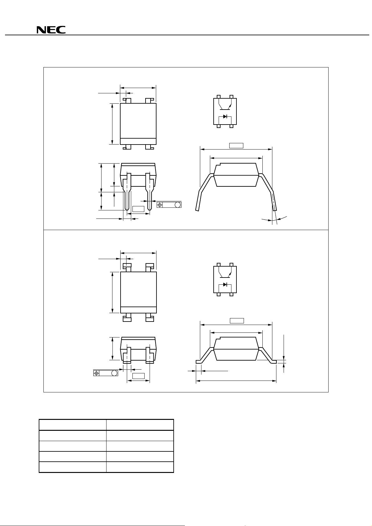
PACKAGE DIMENSIONS (in millimeters)
1.0±0.2
+0.5
4.15±0.4
4.6±0.35
–0.1
6.5
3.5±0.3
PS2581L1
TOP VIEW
3
4
1
2
10.16
7.62
PS2581L1,PS2581L2
1. Anode
2. Cathode
3. Emitter
4. Collector
3.2±0.4
1.25±0.15
1.0±0.2
–0.1
+0.5
6.5
3.5±0.3
1.25±0.15
0.25 M
0.35
2.54
4.6±0.35
2.54
0.50±0.1
0.25 M
PS2581L2
4
1
0.9±0.25
0 to 15˚
TOP VIEW
3
1. Anode
2. Cathode
3. Emitter
4. Collector
2
10.16
7.62
0.25±0.2
12.0 MAX.
PHOTOCOUPLER CONSTRUCTION
Parameter Unit (MIN.)
Air Distance 8 mm
Outer Creepage Distance 8 mm
Inner Creepage Distance 4 mm
Isolation Thickness 0.4 mm
2
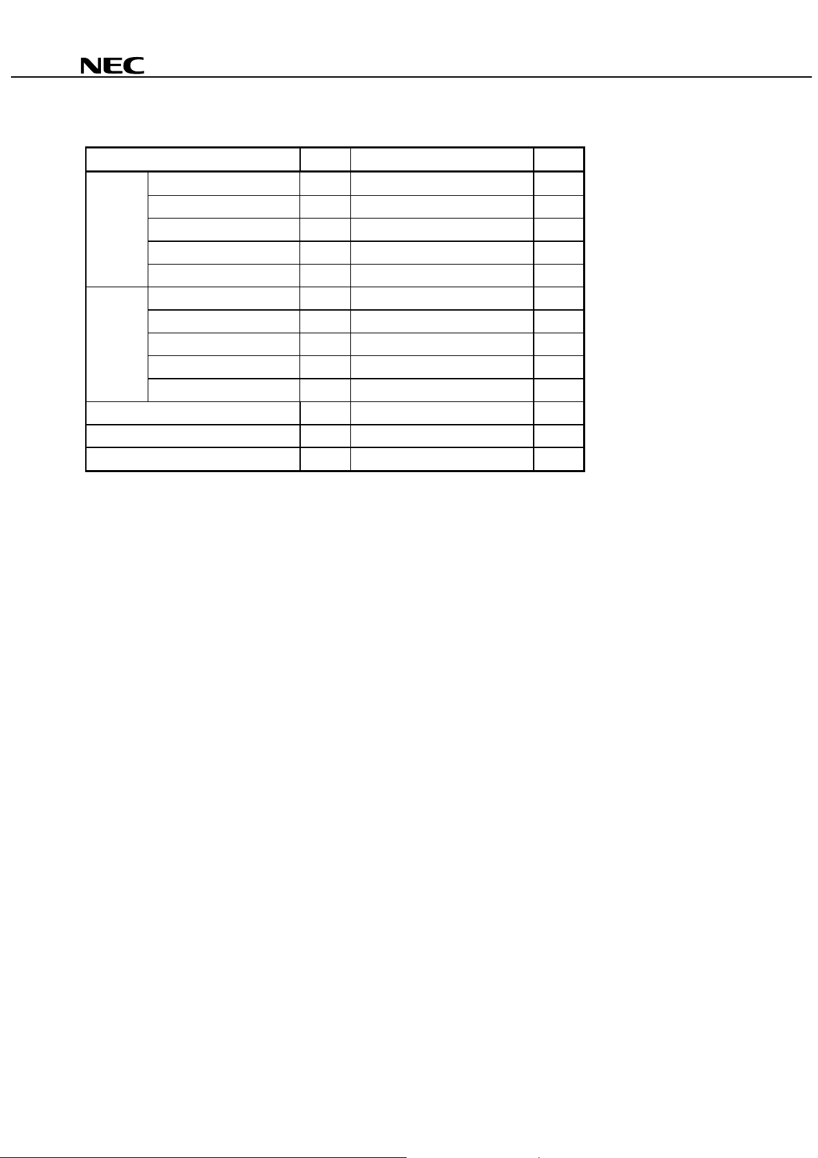
ABSOLUTE MAXIMUM RATINGS (TA = 25 °°°°C, unless otherwise specified)
Parameter Symbol Ratings Unit
PS2581L1,PS2581L2
Diode Forward Current (DC) I
Reverse Voltage V
Power Dissipation Derati ng
Power Dissipation P
Peak Forward Current
*1
Transistor Collector to Emitter Voltage V
Emitter to Collector Voltage V
Collector Current I
Power Dissipation Derati ng
Power Dissipation P
Isolation Voltage
*2
Operating Ambient Temperature T
Storage Temperature
PW = 100
*1
AC voltage for 1 minute at TA = 25 °C, RH = 60 % between input and output
*2
s, Duty Cycle = 1 %
µ
F
R
∆
PD/°C1.5mW/
D
FP
I
CEO
ECO
C
∆
PC/°C1.5mW/
C
80 mA
6V
150 mW
1A
80 V
7V
50 mA
150 mW
BV 5 000 Vr.m.s.
A
stg
T
−
55 to +100
−
55 to +150
°
C
°
C
°
C
°
C
3
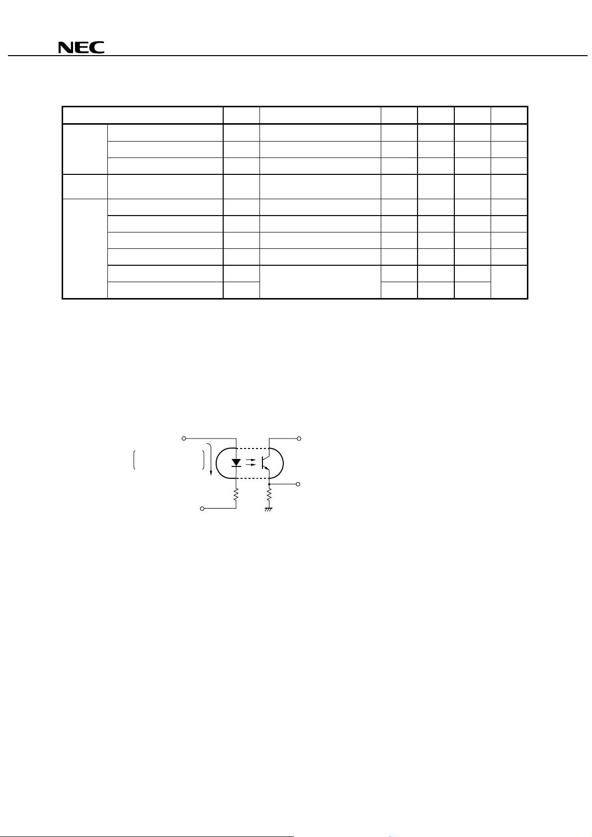
ELECTRICAL CHARACTERISTICS (TA = 25 °°°°C)
Parameter Symbol Conditions MIN. TYP. MAX. Unit
PS2581L1,PS2581L2
Diode Forward Voltage V
Reverse Current I
Terminal Capacitance C
Transistor
Collector to Emitter Dark
Current
*1
Coupled
Current Transfer Ratio (I
C/IF
)
CTR IF = 5 mA, VCE = 5 V 80 200 400 %
Collector Saturation Vol t age V
Isolation Resistance R
Isolation Capacitance C
*2
*2
CTR rank
*1
Rise Time
Fall Time
L : 200 to 400 (%)
M : 80 to 240 (%)
D : 100 to 300 (%)
H : 80 to 160 (%)
W : 130 to 260 (%)
N : 80 to 400 (%)
Test circuit for switching time
*2
F
IF = 10 mA 1.17 1.4 V
R
VR = 5 V 5
t
V = 0 V, f = 1.0 MHz 50 pF
CEO
I
VCE = 80 V, IF = 0 mA 100 nA
CE(sat)IF
t
t
= 10 mA, IC = 2 mA 0.3 V
I-O
I-O
V
= 1.0 kV
I-O
V = 0 V, f = 1.0 MHz 0.5 pF
r
VCC = 10 V, IC = 2 mA, 3
f
RL = 100
DC
Ω
10
11
5
µ
A
Ω
µ
s
Pulse Input
PW = 100 s
µ
Duty Cycle = 1/10
I
F
50 Ω
VCC
VOUT
RL = 100 Ω
4
 Loading...