


NEC PS2601, PS2601L, PS2602L, PS2603L, PS2604 Datasheet
...
California Eastern Laboratories
Optocoupler
Applications

DESIGNING FOR OPTOCOUPLERS WITH BASE PIN
GENERAL
Optocouplers (optical couplers) are designed to isolate electrical output from input for complete elimination of noise. They have
been used conventionally as substitutes for relays and pulse transformers. Today's current technology in the area of microcomputers creates new applications for optocouplers.
This manual describes the characteristics of typical optocouplers. Also included are notes on designing application circuits for
typical optocouplers (with a base pin) for better comprehension. NEC's typical optocouplers with or without base pins are listed
on the following pages.
1
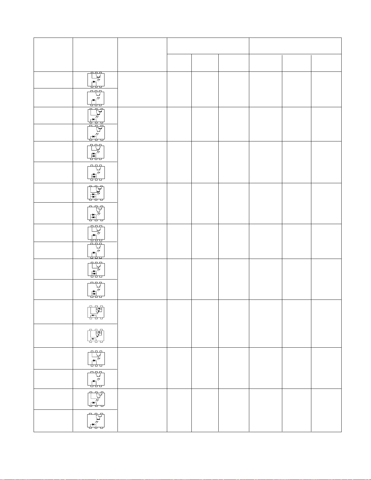
PS2600 Series Optocouplers (6-Pin Dual-in-Line Package)
Absolute Maximum Ratings Electric Characteristics
A = 25°C) (TA = 25°C)
Product name Features
PS2601 High isolation
*
PS2601L voltage
Internal
connection
CEO 5 k 80 50 80 to 600 3 5
High V
PS2602 (80 V MIN.)
PS2602L Single transistor
PS2603 High isolation
*
PS2603L voltage
High CTR 5 k 80 200 200 to 2500 100 100
PS2604 Darlington PS2604L transistor
PS2605 High isolation
*
PS2605L voltage
A.C. input 5 k ±80 50 80 to 600 3 5
CEO
High V
PS2606 (80 V MIN.)
PS2606L Single transistor
PS2607 High isolation
*
PS2607L voltage
A.C. input 5 k ±80 200 200 to 3400 100 100
High CTR
PS2608 Darlington PS2608L transistor
PS2621 High isolation
*
PS2621L voltage
Large input 5 k 150 50 20 to 50 3 5
PS2622 current
PS2622L Single transistor
PS2625 High isolation
*
PS2625L voltage
A.C. input 5 k ±150 50 20 to 50 3 5
Large input
PS2626 current
PS2626L Single transistor
PS2633 High isolation
*
PS2633L voltage
CEO 1000 to
High V
(300 V MIN.) 5 k 80 150 15000 100 100
High CTR
PS2634 Darlington PS2634L transitor
PS2651 High isolation
*
PS2651L2 voltage
CEO 5 k 80 50 50 to 400 3 5
High V
(80 V MIN.)
PS2652 Single transistor
PS2652L2
PS2653 High isolation
*
PS2653L2 voltage
High CTR 5 k 80 200 200 to 3400 100 100
Darlington PS2654 transistors
PS2654L2
(Vr.m.s.) (TYP) (TYP)
(T
BV I
F (mA) IC(mA) CTR (%) tr (µs) tr (µs)
* (with a base pin)
Note: A product name followed by letter L indicates a product having leads formed for surface mount.
2

There are two kinds of optocouplers (a light emitting diode (LED) as an input and a phototransistor as an output) according to the
type of output transistor: Single transistor type and Darlington-transistor type.
The single-transistor type optocouplers are used to perform high-speed switching (with high-speed response). The Darlingtontransistor type optocouplers are used to obtain a large output current by utilizing a small input current (independently of switching
speeds).
Designing the circuits properly will improve the PS2601 optocoupler (Single Transistor type) by having a base pin in terms of
switching speed, elimination of noise in input signals, and output leakage current (collector dark current, and application to highvoltage circuits).
APPLICATIONS OF OPTOCOUPLER BASE PINS
INCREASING SWITCHING SPEED
The switching speed of an optocoupler with a base pin can be increased by inserting a resistor between the base and the emitter
of its phototransistor even when the optocoupler is applied to a large load resistance.
Generally, the phototransistor of an optocoupler such as the PS2601 has a large photo-sensitive area on it. Accordingly, the
junction capacitance (CC-B) between the collector and the base of the phototransistor is great (up to 20 pF) and as a result its
response speed (turn-off time toff) is low. The relationship between turn-off time toff and collector-base capacitance CC-B is
expressed by:
toff × CC-B x hFE x RL ................(1)
where
toff : Turn-off time (See Fig. 2-2.)
CC-B : Collector-base capacitance
hFE : D.C. current amplification factor
RL : Load resistance
Cc-
B
R
L
Figure 2-1. Collector-Base Capacitance
CC-B of Phototransistor
3

Input
monitor
Vo
50%
Input
ton toff
90% 90%
Output
10% 10%
Figure 2-2. ton/toff Measuring Points
As judged from expression (1), the turn-off time toff is affected by collector-base capacitance CC-B, D.C. current amplification
factor hFE, and load resistance LR. In actual circuit design, CC-B and hFE are fixed. Accordingly, the turn-off time is significantly
affected by the resistance of load RL.
Graph 1 shows the relationship between response speed (ton,toff) and load resistance (RL) in typical emitter follower (test circuit 1)
having a load resistance of 100 Ω.
PW = 100 µs
()
Duty = 1/10
VCC = 5 V
PS2601
IF = 5 mA
Input
monitor
51 Ω
Vo
R
L
= 100 Ω
Test Circuit 1
Graph 1
Up : Input 0.2 V/DIV
DOWN : Output 0.5 V/DIV
(50 µs/DIV)
4

Graph 2 shows the relationship between response speed (ton, toff) and load resistance (RL) in a typical emitter follower (Test
circuit 2) having a greater load resistance (5 kΩ).
V
CC
= 5 V
PS2601
IF = 5 mA
Input
monitor
51 Ω
R
L
= 5 Ω
Vo
Input
monitor
Test Circuit 2
Vo
Graph 2
Up : Input 0.2 V/DIV
DOWN : Output 2 V/DIV
(50 µs/DIV)
As shown in Graph 2, the turn-off time for load resistance of 5 kΩ is about 100 µs. Similarly, the turn-off time for load resistance
of 100 kΩ is 1 to 2 ms. This is also true when the load resistance is connected to the collector of the phototransistor.
Graph 3 shows the relationship between response speed (t
on, toff) and load resistance (RL) in a typical circuit (Test circuit 3)
having collector load resistance (5 kΩ) with the emitter grounded.
V
CC
= 5 V
R
L
= 5 Ω
PS2601
IF = 5 mA
Input
monitor
51 Ω
Vo
Input
monitor
Vo
Test Circuit 3
Graph 3
Up : Input 0.2 V/DIV
DOWN : Output 2 V/DIV
(50 µs/DIV)
5

Input
monitor
Vo
To reduce the turn-off time toff of a test circuit having a greater resistance, insert a resistor RBE between the emitter and the base
of the phototransistor. See Test circuit 4 and Test circuit 5. Graph 4 and 5 show their input and output waveforms.
V
CC
= 5 V
PS2601
IF = 5 mA
Input
Input
monitor
Vo
monitor
Insert resistor
of 200 kΩ here.
Test Circuit 4
(Emitter Follower)
51 Ω
R
BE
PS2601
R
R
L
= 5 Ω
L
= 5 Ω
Vo
Vo
Graph 4
Up : Input 0.2 V/DIV
DOWN : Output 2 V/DIV
(50 µs/DIV)
V
CC
= 5 V
IF = 5 mA
Input
monitor
Insert resistor
of 200 kΩ here.
Test Circuit 5
(Emitter Grounded)
51 Ω
R
BE
Graph 5
Up : Input 0.2 V/DIV
DOWN : Output 2 V/DIV
6
(50 µs/DIV)

The turn-off time can be greatly reduced by the base-emitter resistance (RL). In Test circuit 4, the turn-off time of the test circuit
having resistance RL is about 1/30 of that of the test circuit without the resistance. This is because the carrier (photocurrent)
stored in the collector-base capacitor (CC-B) is quickly released through the base-emitter resistor (RBE). However, note that part
of a photocurrent generating on the base of the phototransistor flows through the R
BE resistor and reduces the current transfer
ratio (CTR). Compare the voltage level of the output waveform in Photo 4 with that of the output waveform in Photo 2. The
current transfer ratio of the test circuit having a base-emitter resistor of 200 kΩ is half or less of that of the test circuit without the
resistance. (See 3.3 for reduction of the current transfer ratio CTR.)
For reference, Fig. 2-3 shows the switching-time vs. R
L characteristics and Fig. 2-4 shows the switching-time vs. RBE characteris-
tics.
1000
I
F =
5 mA
500
51Ω
200
I
F
= 5 mA VCC = 5 V
Sample Solid line:
Current transfer ratio of 166%
100
Dotted line:
Current transfer ratio of 274%
at Ir = 5 mA
50
VCC = 5V
x
I
Vo
R
L
t
f
t
s
20
10
Switching Time (µs)
5
2
1
100 500 1 k 5 k 10 k 50 k 100 k
Load Resistance RL (Ω)
Fig. 2-3 Switching-Time vs. RL Characteristics
1000
I
F =
10 mA
500
IF = 10 mA Vcc = 5 V
200
Sample Solid line:
Current transfer ratio of 166%
100
Current transfer ratio of 274%
at Ir = 5mA
51Ω
x
I
Dotted line:
Vcc = 5V
L
R
Vo
t f
t s
50
20
10
t
r
t
d
Switching Time (µs)
5
2
t r
t d
1
100 500 1 k 5 k 10 k 50 k 100 k
Load Resistance RL (Ω)
160
Vcc = 5 V, IF = 5mA
R
140
1 = 5Ω
Solid line: Emitter follower
Dotted line: Emitter grounded
120
100
80
60
Switching Time (µs)
40
ton
20
0
100 200 500 1000
Base-Emitter Resistance RBE (kΩ)
Fig. 2-4 Switching-Time vs. RBE Characteristics
160
VCC = 5 V, IF = 10mA
R
L
140
= 5Ω
Solid line: Emitter follower
Dotted line: Emitter grounded
120
100
t
toff
off
80
60
Switching Time (µs)
40
t
20
off
0
8
100 200 500 1000
8
Base-Emitter Resistance RBE (kΩ)
7

STABILIZING OUTPUT LEVELS
When an optocoupler is used with the base pin of its phototransistor open, the collector dark current (ICEO) flows as a base
current. The current is amplified as a collector current and could make the output level of the phototransistor unstable. To
eliminate this unwanted base current and make the output level stable, flow the collector dark current (I
emitter resistor (RBE).
Fig 2-5 shows the I
CEO vs. TA characteristics of a PS2601 optocoupler .
PS2601 ICEO-TA Characteristics
10000
IF = 0
V
CE
= 80V (40V for the
PS2603) 2601
(nA)
CEO
Solid line: PS2601
Dotted line: PS2603
1000
100
10
8
R
BE
=
RBE = 1M
R
BE
=1M
Ω
Ω
CEO) through the base-
1
R
BE
=100 M
Ω
Collector Dark Current I
0.1
- 20 0 20
40 60 80 100
Ambient T emperature TA (°C)
Figure 2-5. I
CEO vs. TA Characteristics
ELIMINATION OF INDUCED NOISE
Generally, machine-controlling equipment generates induced noise which may cause malfunctions. This unwanted noise in input
signals can be isolated by means of optocouplers. However, if the noise is too strong, it may be switched to the output through
the input-output capacitance C1-2 of the optocoupler. This unwanted noise in the output can be removed in the following manner.
Insert a capacitor (preferably 100 pF) between the base and the emitter of the phototransistor of the optocoupler. This capacitor
delays response and suppresses malfunctions.
Graph 6-(a) to 6-(d) show how an external noise (surge voltage of 1000 V/µs at rise time) is eliminated as the capacitance of the
base-emitter capacitor.
A fluctuation in the collector-emitter voltage caused by the on/off operation of a power switch at the output of the optocoupler
causes a base current to flow through the collector-base capacitor (CCB), which causes a malfunction.
In Fig. 2-7, for example, an instantaneous base current flows through the collector-base capacitor (CCB) of the optocoupler. The
current is multiplied by hFE (as a collector current) and causes an output voltage on both ends of the load resistance. It seems as
if an input signal was applied to the optocoupler. Graph 7-(a) shows the waveforms. This unwanted instantaneous induction
current can be eliminated by inserting a capacitor CBE between the emitter and the base of the phototransistor. Graph 7-(b)
shows the waveforms. Fig. 2-8 shows the output-voltage vs. CBE characteristics.
Figure 2-6.
V
o
C
BE
R
L
Figure 2-7.
8

6a) CBE = No capacitance
Vo
Vin
6b) CBE = 10 pF
Vin
Vo
6d) CBE = 1000 pF
Vin
Vin
Vo
6c) C
BE = 100 pF
Vo
Graph 6
Up : Input Surge Voltage (Vin :1000 V/DIV)
DOWN : PS2601 output (VO: 1 V/DIV)
Vin
C
1-2
CBE
Test Circuit
9
5 V
Vo
470 Ω

Vin (dV/dt = 10 V/µs, 2 V/DIV)
CCB
Vin
Vo
(500 ns/DIV)
Graph 7-(a)
Input Voltage Fluctuation and Output
Vo (0.1 V/DIV)
Vin (dV/dt = 10 V/µs, 2 V/DIV)
Vo (0.1 V/DIV)
1000 pF
5 kΩ
C
CB
5 kΩ
Vin
Vo
(500 ns/DIV)
Graph 7-(b)
Effect of Collector-Base Capacitance on
Voltage Fluctuation
10

0.1
Output Voltage, Vo (V)
0.01
PS2601
R
L
1
= 5 kΩ
100 1000
Base-Emitter Capacitance, CBE (pF)
Figure 2-8. Vo vs. CBE Characteristics
As mentioned above, noise induced by the fluctuation of supply voltage can be removed by proper treatment of the base pin. For
switching of input free from induced noise at normal switching speed, optocouplers with a base pin such as the PS2602 series
are available. If the base pin of an optocoupler is left unused or opened, it typically will pick up external noise. Cutting off the
base pin is also effective in order to prevent it from picking up external noise. See Graph 8-(b).
11
 Loading...