


User’s Manual
V850ES/HJ2
32-bit Single-Chip Microcontrollers
Hardware
μ
PD70F3709
μ
PD70F3710
μ
PD70F3711
μ
PD70F3712
Document No. U17717EJ3V0UD00 (3rd edition)
Date Published March 2007 N CP(K)
Printed in Japan
2005

[MEMO]
2
User’s Manual U17717EJ3V0UD

NOTES FOR CMOS DEVICES
1
VOLTAGE APPLICATION WAVEFORM AT INPUT PIN
Waveform distortion due to input noise or a reflected wave may cause malfunction. If the input of the
IL
CMOS device stays in the area between V
malfunction. Take care to prevent chattering noise from entering the device when the input level is fixed,
and also in the transition period when the input level passes through the area between V
V
IH
(MIN).
HANDLING OF UNUSED INPUT PINS
2
Unconnected CMOS device inputs can be cause of malfunction. If an input pin is unconnected, it is
possible that an internal input level may be generated due to noise, etc., causing malfunction. CMOS
devices behave differently than Bipolar or NMOS devices. Input levels of CMOS devices must be fixed
high or low by using pull-up or pull-down circuitry. Each unused pin should be connected to V
via a resistor if there is a possibility that it will be an output pin. All handling related to unused pins must
be judged separately for each device and according to related specifications governing the device.
3
PRECAUTION AGAINST ESD
A strong electric field, when exposed to a MOS device, can cause destruction of the gate oxide and
ultimately degrade the device operation. Steps must be taken to stop generation of static electricity as
much as possible, and quickly dissipate it when it has occurred. Environmental control must be
adequate. When it is dry, a humidifier should be used. It is recommended to avoid using insulators that
easily build up static electricity. Semiconductor devices must be stored and transported in an anti-static
container, static shielding bag or conductive material. All test and measurement tools including work
benches and floors should be grounded. The operator should be grounded using a wrist strap.
Semiconductor devices must not be touched with bare hands. Similar precautions need to be taken for
PW boards with mounted semiconductor devices.
(MAX) and VIH (MIN) due to noise, etc., the device may
IL
(MAX) and
DD
or GND
4
STATUS BEFORE INITIALIZATION
Power-on does not necessarily define the initial status of a MOS device. Immediately after the power
source is turned ON, devices with reset functions have not yet been initialized. Hence, power-on does
not guarantee output pin levels, I/O settings or contents of registers. A device is not initialized until the
reset signal is received. A reset operation must be executed immediately after power-on for devices
with reset functions.
5
POWER ON/OFF SEQUENCE
In the case of a device that uses different power supplies for the internal operation and external
interface, as a rule, switch on the external power supply after switching on the internal power supply.
When switching the power supply off, as a rule, switch off the external power supply and then the
internal power supply. Use of the reverse power on/off sequences may result in the application of an
overvoltage to the internal elements of the device, causing malfunction and degradation of internal
elements due to the passage of an abnormal current.
The correct power on/off sequence must be judged separately for each device and according to related
specifications governing the device.
6
INPUT OF SIGNAL DURING POWER OFF STATE
Do not input signals or an I/O pull-up power supply while the device is not powered. The current
injection that results from input of such a signal or I/O pull-up power supply may cause malfunction and
the abnormal current that passes in the device at this time may cause degradation of internal elements.
Input of signals during the power off state must be judged separately for each device and according to
related specifications governing the device.
User’s Manual U17717EJ3V0UD
3

IECUBE is a registered trademark of NEC Electronics Corporation in Japan and Germany.
MINICUBE is a registered trademark of NEC Electronics Corporation in Japan and Germany or a
trademark in the United States of America.
Applilet is a registered trademark of NEC Electronics in Japan, Germany, Hong Kong, China, the Republic of
Korea, the United Kingdom, and the United States of America.
Windows and Windows NT are either registered trademarks or trademarks of Microsoft Corporation in
the United States and/or other countries.
PC/AT is a trademark of International Business Machines Corporation.
SPARCstation is a trademark of SPARC International, Inc.
Solaris and SunOS are trademarks of Sun Microsystems, Inc.
TRON is an abbreviation of The Real-Time Operating system Nucleus.
ITRON is an abbreviation of Industrial TRON.
4
User’s Manual U17717EJ3V0UD

•
The information in this document is current as of August, 2006. The information is subject to
change without notice. For actual design-in, refer to the latest publications of NEC Electronics data
sheets or data books, etc., for the most up-to-date specifications of NEC Electronics products. Not
all products and/or types are available in every country. Please check with an NEC Electronics sales
representative for availability and additional information.
No part of this document may be copied or reproduced in any form or by any means without the prior
•
written consent of NEC Electronics. NEC Electronics assumes no responsibility for any errors that may
appear in this document.
•
NEC Electronics does not assume any liability for infringement of patents, copyrights or other intellectual
property rights of third parties by or arising from the use of NEC Electronics products listed in this document
or any other liability arising from the use of such products. No license, express, implied or otherwise, is
granted under any patents, copyrights or other intellectual property rights of NEC Electronics or others.
Descriptions of circuits, software and other related information in this document are provided for illustrative
•
purposes in semiconductor product operation and application examples. The incorporation of these
circuits, software and information in the design of a customer's equipment shall be done under the full
responsibility of the customer. NEC Electronics assumes no responsibility for any losses incurred by
customers or third parties arising from the use of these circuits, software and information.
•
While NEC Electronics endeavors to enhance the quality, reliability and safety of NEC Electronics products,
customers agree and acknowledge that the possibility of defects thereof cannot be eliminated entirely. To
minimize risks of damage to property or injury (including death) to persons arising from defects in NEC
Electronics products, customers must incorporate sufficient safety measures in their design, such as
redundancy, fire-containment and anti-failure features.
NEC Electronics products are classified into the following three quality grades: "Standard", "Special" and
•
"Specific".
The "Specific" quality grade applies only to NEC Electronics products developed based on a customerdesignated "quality assurance program" for a specific application. The recommended applications of an NEC
Electronics product depend on its quality grade, as indicated below. Customers must check the quality grade of
each NEC Electronics product before using it in a particular application.
"Standard": Computers, office equipment, communications equipment, test and measurement equipment, audio
and visual equipment, home electronic appliances, machine tools, personal electronic equipment
and industrial robots.
"Special": Transportation equipment (automobiles, trains, ships, etc.), traffic control systems, anti-disaster
systems, anti-crime systems, safety equipment and medical equipment (not specifically designed
for life support).
"Specific": Aircraft, aerospace equipment, submersible repeaters, nuclear reactor control systems, life
support systems and medical equipment for life support, etc.
The quality grade of NEC Electronics products is "Standard" unless otherwise expressly specified in NEC
Electronics data sheets or data books, etc. If customers wish to use NEC Electronics products in applications
not intended by NEC Electronics, they must contact an NEC Electronics sales representative in advance to
determine NEC Electronics' willingness to support a given application.
(Note)
(1) "NEC Electronics" as used in this statement means NEC Electronics Corporation and also includes its
majority-owned subsidiaries.
(2) "NEC Electronics products" means any product developed or manufactured by or for NEC Electronics (as
defined above).
M8 E 02 . 11-1
User’s Manual U17717EJ3V0UD
5

PREFACE
Readers This manual is intended for users who wish to understand the functions of the
V850ES/HJ2 and design application systems using the V850ES/HJ2.
Purpose This manual is intended to give users an understanding of the hardware functions of
the V850ES/HJ2 shown in the Organization below.
Organization This manual is divided into two parts: Hardware (this manual) and Architecture
(V850ES Architecture User’s Manual).
Hardware Architecture
• Pin functions • Data types
• CPU function • Register set
• On-chip peripheral functions • Instruction format and instruction set
• Flash memory programming • Interrupts and exceptions
• Electrical specifications • Pipeline operation
How to Read This Manual It is assumed that the readers of this manual have general knowledge in the fields of
electrical engineering, logic circuits, and microcontrollers.
To understand the overall functions of the V850ES/HJ2
→ Read this manual according to the CONTENTS.
To find the details of a register where the name is known
→ Use APPENDIX B REGISTER INDEX.
To understand the details of an instruction function
→ Refer to the V850ES Architecture User’s Manual available separately.
To know the electrical specifications of the V850ES/HJ2
→ See CHAPTER 27 ELECTRICAL SPECIFICATIONS.
The “yyy bit of the xxx register” is described as the “xxx.yyy bit” in this manual. Note
with caution that if “xxx.yyy” is described as is in a program, however, the
compiler/assembler cannot recognize it correctly.
The mark <R> shows major revised points. The revised points can be easily
searched by copying an “<R>” in the PDF file and specifying it in the “Find what:” field.
6
User’s Manual U17717EJ3V0UD

Conventions Data significance: Higher digits on the left and lower digits on the right
Active low representation: xxx (overscore over pin or signal name)
Memory map address: Higher addresses on the top and lower addresses on
the bottom
Note: Footnote for item marked with Note in the text
Caution: Information requiring particular attention
Remark: Supplementary information
Numeric representation: Binary ... xxxx or xxxxB
Decimal ... xxxx
Hexadecimal ... xxxxH
Prefix indicating power of 2
(address space, memory
capacity): K (kilo): 2
M (mega): 2
G (giga): 2
10
= 1,024
20
= 1,0242
30
= 1,0243
User’s Manual U17717EJ3V0UD
7
Related Documents The related documents indicated in this publication may include preliminary versions.
However, preliminary versions are not marked as such.
Documents related to V850ES/HJ2
Document Name Document No.
V850ES Architecture User’s Manual U15943E
V850ES/HJ2 Hardware User’s Manual This manual
Documents related to development tools (user’s manuals)
Document Name Document No.
QB-V850MINI On-Chip Debug Emulator U17638E
QB-MINI2 On-Chip Debug Emulator with Flash Programming Function To be prepared
CA850 Ver. 3.00 C Compiler Package
PM+ Ver. 6.20 Project Manager U17990E
ID850QB Ver. 3.20 Integrated Debugger Operation U17964E
SM850 Ver. 2.50 System Simulator Operation U16218E
SM850 Ver. 2.00 or Later System Simulator External Part User Open
RX850 Ver. 3.20 Real-Time OS
RX850 Pro Ver. 3.20 Real-Time OS
AZ850 Ver. 3.30 System Performance Analyzer U17423E
PG-FP4 Flash Memory Programmer U15260E
Operation U17293E
C Language U17291E
Assembly Language U17292E
Link Directives U17294E
U14873E
Interface Specification
Operation U17246E SM+ System Simulator
User Open Interface
Specification
Basics U13430E
Installation U17419E
Technical U13431E
Task Debugger U17420E
Basics U13773E
Installation U17421E
Technical U13772E
Task Debugger U17422E
U17247E
8
User’s Manual U17717EJ3V0UD

CONTENTS
CHAPTER 1 INTRODUCTION .................................................................................................................18
1.1 General .....................................................................................................................................18
1.2 Features....................................................................................................................................20
1.3 Application Fields ...................................................................................................................21
1.4 Ordering Information ..............................................................................................................21
1.5 Pin Configuration (Top View).................................................................................................22
1.6 Function Block Configuration................................................................................................ 24
1.6.1 Internal block diagram ............................................................................................................... 24
1.6.2 Internal units .............................................................................................................................. 25
CHAPTER 2 PIN FUNCTIONS................................................................................................................27
2.1 Pin Function List .....................................................................................................................27
2.2 Pin Status ................................................................................................................................. 35
2.3 Description of Pin Functions .................................................................................................36
2.4 Pin I/O Circuit Types and Recommended Connection of Unused Pins ............................45
2.5 Pin I/O Circuits......................................................................................................................... 48
2.6 Cautions ...................................................................................................................................49
CHAPTER 3 CPU FUNCTION.................................................................................................................50
3.1 Features....................................................................................................................................50
3.2 CPU Register Set.....................................................................................................................51
3.2.1 Program register set .................................................................................................................. 52
3.2.2 System register set .................................................................................................................... 53
3.3 Operation Modes .....................................................................................................................59
3.3.1 Specifying operation mode ........................................................................................................59
3.4 Address Space ........................................................................................................................60
3.4.1 CPU address space................................................................................................................... 60
3.4.2 Wraparound of CPU address space .......................................................................................... 61
3.4.3 Memory map.............................................................................................................................. 62
3.4.4 Areas .........................................................................................................................................64
3.4.5 Recommended use of address space ....................................................................................... 68
3.4.6 Peripheral I/O registers.............................................................................................................. 71
3.4.7 Special registers ........................................................................................................................ 82
3.4.8 Cautions .................................................................................................................................... 86
CHAPTER 4 PORT FUNCTIONS............................................................................................................89
4.1 Features....................................................................................................................................89
4.2 Basic Configuration of Ports .................................................................................................89
4.3 Port Functions .........................................................................................................................91
4.3.1 Operation of port function ..........................................................................................................91
4.3.2 Notes on setting port pins ..........................................................................................................92
4.3.3 Port 0 ......................................................................................................................................... 93
4.3.4 Port 1 ......................................................................................................................................... 97
4.3.5 Port 3 ....................................................................................................................................... 100
4.3.6 Port 4 ....................................................................................................................................... 106
User’s Manual U17717EJ3V0UD
9

4.3.7 Port 5 .......................................................................................................................................109
4.3.8 Port 6 .......................................................................................................................................115
4.3.9 Port 7 .......................................................................................................................................122
4.3.10 Port 8 ....................................................................................................................................... 124
4.3.11 Port 9 ....................................................................................................................................... 127
4.3.12 Port 12 ..................................................................................................................................... 137
4.3.13 Port CD....................................................................................................................................139
4.3.14 Port CM ...................................................................................................................................141
4.3.15 Port CS .................................................................................................................................... 144
4.3.16 Port CT ....................................................................................................................................147
4.3.17 Port DL ....................................................................................................................................150
4.3.18 Port pins that function alternately as on-chip debug function...................................................153
4.3.19 Register settings to use port pins as alternate-function pins....................................................154
4.4 Block Diagrams of Port........................................................................................................ 161
4.5 Cautions ................................................................................................................................ 190
4.5.1 Cautions on setting port pins ................................................................................................... 190
CHAPTER 5 BUS CONTROL FUNCTION .......................................................................................... 191
5.1 Features................................................................................................................................. 191
5.2 Bus Control Pins................................................................................................................... 192
5.2.1 Pin status when internal ROM, internal RAM, or on-chip peripheral I/O is accessed ............... 192
5.2.2 Pin status in each operation mode ........................................................................................... 192
5.3 Memory Block Function....................................................................................................... 193
5.4 Bus Access ........................................................................................................................... 194
5.4.1 Number of clocks for access .................................................................................................... 194
5.4.2 Bus size setting function ..........................................................................................................194
5.4.3 Access by bus size ..................................................................................................................195
5.5 Wait Function ........................................................................................................................ 202
5.5.1 Programmable wait function ....................................................................................................202
5.5.2 External wait function ............................................................................................................... 203
5.5.3 Relationship between programmable wait and external wait ...................................................203
5.5.4 Programmable address wait function ....................................................................................... 204
5.6 Idle State Insertion Function ............................................................................................... 205
5.7 Bus Hold Function................................................................................................................ 206
5.7.1 Functional outline.....................................................................................................................206
5.7.2 Bus hold procedure.................................................................................................................. 207
5.7.3 Operation in power save mode ................................................................................................207
5.8 Bus Priority ........................................................................................................................... 208
5.9 Bus Timing ............................................................................................................................ 209
CHAPTER 6 CLOCK GENERATION FUNCTION .............................................................................. 212
6.1 Overview................................................................................................................................ 212
6.2 Configuration ........................................................................................................................ 213
6.3 Registers ............................................................................................................................... 215
6.4 Operation............................................................................................................................... 220
6.4.1 Operation of each clock ...........................................................................................................220
6.4.2 Clock output function ...............................................................................................................220
6.5 PLL Function......................................................................................................................... 221
10
User’s Manual U17717EJ3V0UD

6.5.1 Overview ................................................................................................................................. 221
6.5.2 Registers ................................................................................................................................. 221
6.5.3 Usage ......................................................................................................................................225
CHAPTER 7 16-BIT TIMER/EVENT COUNTER P (TMP) .................................................................226
7.1 Overview.................................................................................................................................226
7.2 Functions ...............................................................................................................................226
7.3 Configuration.........................................................................................................................227
7.4 Registers ................................................................................................................................229
7.5 Operation................................................................................................................................243
7.5.1 Interval timer mode (TPnMD2 to TPnMD0 bits = 000) ............................................................. 244
7.5.2 External event count mode (TPnMD2 to TPnMD0 bits = 001) ................................................. 254
7.5.3 External trigger pulse output mode (TPnMD2 to TPnMD0 bits = 010) ..................................... 262
7.5.4 One-shot pulse output mode (TPnMD2 to TPnMD0 bits = 011) .............................................. 274
7.5.5 PWM output mode (TPnMD2 to TPnMD0 bits = 100).............................................................. 281
7.5.6 Free-running timer mode (TPnMD2 to TPnMD0 bits = 101) .................................................... 290
7.5.7 Pulse width measurement mode (TPnMD2 to TPnMD0 bits = 110) ........................................ 307
7.5.8 Timer output operations........................................................................................................... 313
7.6 Timer Tuned Operation Function ........................................................................................314
7.7 Selector Function ..................................................................................................................318
7.8 Cautions .................................................................................................................................320
CHAPTER 8 16-BIT TIMER/EVENT COUNTER Q (TMQ) ................................................................321
8.1 Overview.................................................................................................................................321
8.2 Functions ...............................................................................................................................321
8.3 Configuration.........................................................................................................................322
8.4 Registers ................................................................................................................................325
8.5 Operation................................................................................................................................343
8.5.1 Interval timer mode (TQnMD2 to TQnMD0 bits = 000) ............................................................ 344
8.5.2 External event count mode (TQnMD2 to TQnMD0 bits = 001) ................................................ 353
8.5.3 External trigger pulse output mode (TQnMD2 to TQnMD0 bits = 010) .................................... 362
8.5.4 One-shot pulse output mode (TQnMD2 to TQnMD0 bits = 011) ............................................. 375
8.5.5 PWM output mode (TQnMD2 to TQnMD0 bits = 100) ............................................................. 384
8.5.6 Free-running timer mode (TQnMD2 to TQnMD0 bits = 101) ................................................... 395
8.5.7 Pulse width measurement mode (TQnMD2 to TQnMD0 bits = 110)........................................ 415
8.5.8 Triangular wave PWM mode (TQnMD2 to TQnMD0 = 111) .................................................... 421
8.5.9 Timer output operations........................................................................................................... 422
8.6 Timer Tuned Operation Function ........................................................................................423
8.7 Cautions .................................................................................................................................427
CHAPTER 9 16-BIT INTERVAL TIMER M (TMM).............................................................................428
9.1 Overview.................................................................................................................................428
9.2 Configuration.........................................................................................................................429
9.3 Register ..................................................................................................................................430
9.4 Operation................................................................................................................................431
9.4.1 Interval timer mode .................................................................................................................. 431
9.4.2 Cautions .................................................................................................................................. 435
User’s Manual U17717EJ3V0UD
11

CHAPTER 10 WATCH TIMER FUNCTIONS ...................................................................................... 436
10.1 Functions............................................................................................................................... 436
10.2 Configuration ........................................................................................................................ 437
10.3 Registers ............................................................................................................................... 439
10.4 Operation............................................................................................................................... 443
10.4.1 Operation as watch timer......................................................................................................... 443
10.4.2 Operation as interval timer....................................................................................................... 444
10.4.3 Cautions...................................................................................................................................445
CHAPTER 11 FUNCTIONS OF WATCHDOG TIMER 2 ................................................................... 446
11.1 Functions............................................................................................................................... 446
11.2 Configuration ........................................................................................................................ 447
11.3 Registers ............................................................................................................................... 448
11.4 Operation............................................................................................................................... 451
CHAPTER 12 A/D CONVERTER ......................................................................................................... 452
12.1 Overview................................................................................................................................ 452
12.2 Functions............................................................................................................................... 452
12.3 Configuration ........................................................................................................................ 453
12.4 Registers ............................................................................................................................... 456
12.5 Operation............................................................................................................................... 464
12.5.1 Basic operation ........................................................................................................................ 464
12.5.2 Trigger mode ...........................................................................................................................465
12.5.3 Operation mode ....................................................................................................................... 467
12.5.4 Power-fail compare mode ........................................................................................................ 471
12.6 Cautions ................................................................................................................................ 476
12.7 How to Read A/D Converter Characteristics Table........................................................... 480
CHAPTER 13 ASYNCHRONOUS SERIAL INTERFACE A (UARTA) ............................................. 484
13.1 Features................................................................................................................................. 485
13.2 Configuration ........................................................................................................................ 486
13.3 Registers ............................................................................................................................... 488
13.4 Interrupt Request Signals.................................................................................................... 494
13.5 Operation............................................................................................................................... 495
13.5.1 Data format..............................................................................................................................495
13.5.2 SBF transmission/reception format..........................................................................................497
13.5.3 SBF transmission.....................................................................................................................499
13.5.4 SBF reception .......................................................................................................................... 500
13.5.5 UART transmission..................................................................................................................501
13.5.6 Continuous transmission procedure.........................................................................................502
13.5.7 UART reception .......................................................................................................................504
13.5.8 Reception errors ...................................................................................................................... 505
13.5.9 Parity types and operations .....................................................................................................507
13.5.10 Receive data noise filter...........................................................................................................508
13.6 Dedicated Baud Rate Generator ......................................................................................... 509
13.7 Cautions ................................................................................................................................ 517
CHAPTER 14 3-WIRE VARIABLE-LENGTH SERIAL I/O (CSIB).................................................... 518
12
User’s Manual U17717EJ3V0UD

14.1
Features..................................................................................................................................518
14.2 Configuration.........................................................................................................................519
14.3 Registers ................................................................................................................................521
14.4 Interrupt Request Signals.....................................................................................................528
14.5 Operation................................................................................................................................529
14.5.1 Single transfer mode (master mode, transmission mode) .......................................................529
14.5.2 Single transfer mode (master mode, reception mode)............................................................. 531
14.5.3 Single transfer mode (master mode, transmission/reception mode)........................................ 533
14.5.4 Single transfer mode (slave mode, transmission mode).......................................................... 535
14.5.5 Single transfer mode (slave mode, reception mode) ...............................................................537
14.5.6 Single transfer mode (slave mode, transmission/reception mode) ..........................................539
14.5.7 Continuous transfer mode (master mode, transmission mode) ............................................... 541
14.5.8 Continuous transfer mode (master mode, reception mode)..................................................... 543
14.5.9 Continuous transfer mode (master mode, transmission/reception mode)................................ 546
14.5.10 Continuous transfer mode (slave mode, transmission mode).................................................. 550
14.5.11 Continuous transfer mode (slave mode, reception mode) ....................................................... 552
14.5.12 Continuous transfer mode (slave mode, transmission/reception mode) .................................. 555
14.5.13 Reception error........................................................................................................................ 559
14.5.14 Clock timing............................................................................................................................. 560
14.6 Output Pin Status with Operation Disabled .......................................................................562
14.7 Baud Rate Generator ............................................................................................................563
14.7.1 Baud rate generation ............................................................................................................... 564
14.8 Cautions .................................................................................................................................565
CHAPTER 15 DMA FUNCTION (DMA CONTROLLER) ....................................................................566
15.1 Features..................................................................................................................................566
15.2 Configuration.........................................................................................................................567
15.3 Registers ................................................................................................................................568
15.4 Transfer Targets .................................................................................................................... 576
15.5 Transfer Modes......................................................................................................................576
15.6 Transfer Types.......................................................................................................................577
15.7 DMA Channel Priorities ........................................................................................................578
15.8 Time Related to DMA Transfer.............................................................................................578
15.9 DMA Transfer Start Factors .................................................................................................579
15.10 DMA Abort Factors................................................................................................................ 580
15.11 End of DMA Transfer.............................................................................................................580
15.12 Operation Timing................................................................................................................... 580
15.13 Cautions .................................................................................................................................585
CHAPTER 16 INTERRUPT/EXCEPTION PROCESSING FUNCTION ...............................................590
16.1 Features..................................................................................................................................590
16.2 Non-Maskable Interrupts ......................................................................................................594
16.2.1 Operation................................................................................................................................. 596
16.2.2 Restore.................................................................................................................................... 597
16.2.3 NP flag..................................................................................................................................... 598
16.3 Maskable Interrupts ..............................................................................................................599
16.3.1 Operation................................................................................................................................. 599
16.3.2 Restore.................................................................................................................................... 601
User’s Manual U17717EJ3V0UD
13

16.3.3 Priorities of maskable interrupts...............................................................................................602
16.3.4 Interrupt control register (xxICn) ..............................................................................................606
16.3.5 Interrupt mask registers 0 to 4 (IMR0 to IMR4)........................................................................ 608
16.3.6 In-service priority register (ISPR).............................................................................................610
16.3.7 ID flag ......................................................................................................................................611
16.3.8 Watchdog timer mode register 2 (WDTM2) .............................................................................611
16.4 Software Exception .............................................................................................................. 612
16.4.1 Operation................................................................................................................................. 612
16.4.2 Restore ....................................................................................................................................613
16.4.3 EP flag ..................................................................................................................................... 614
16.5 Exception Trap...................................................................................................................... 615
16.5.1 Illegal opcode definition ...........................................................................................................615
16.5.2 Debug trap ............................................................................................................................... 617
16.6 External Interrupt Request Input Pins (NMI and INTP0 to INTP14) ................................. 619
16.6.1 Noise elimination .....................................................................................................................619
16.6.2 Edge detection.........................................................................................................................619
16.7 Interrupt Acknowledge Time of CPU .................................................................................. 628
16.8 Periods in Which Interrupts Are Not Acknowledged by CPU.......................................... 629
16.9 Cautions ................................................................................................................................ 629
CHAPTER 17 KEY INTERRUPT FUNCTION ..................................................................................... 630
17.1 Function................................................................................................................................. 630
17.2 Register ................................................................................................................................. 631
17.3 Cautions ................................................................................................................................ 631
CHAPTER 18 STANDBY FUNCTION .................................................................................................. 632
18.1 Overview................................................................................................................................ 632
18.2 Registers ............................................................................................................................... 634
18.3 HALT Mode............................................................................................................................ 637
18.3.1 Setting and operation status ....................................................................................................637
18.3.2 Releasing HALT mode............................................................................................................. 637
18.4 IDLE1 Mode ........................................................................................................................... 639
18.4.1 Setting and operation status ....................................................................................................639
18.4.2 Releasing IDLE1 mode............................................................................................................ 639
18.5 IDLE2 Mode ........................................................................................................................... 641
18.5.1 Setting and operation status ....................................................................................................641
18.5.2 Releasing IDLE2 mode............................................................................................................ 641
18.5.3 Securing setup time when releasing IDLE2 mode ...................................................................643
18.6 STOP Mode............................................................................................................................ 644
18.6.1 Setting and operation status ....................................................................................................644
18.6.2 Releasing STOP mode ............................................................................................................644
18.6.3 Securing oscillation stabilization time when releasing STOP mode ......................................... 646
18.7 Subclock Operation Mode ................................................................................................... 647
18.7.1 Setting and operation status ....................................................................................................647
18.7.2 Releasing subclock operation mode ........................................................................................647
18.8 Sub-IDLE Mode ..................................................................................................................... 649
18.8.1 Setting and operation status ....................................................................................................649
18.8.2 Releasing sub-IDLE mode ....................................................................................................... 650
14
User’s Manual U17717EJ3V0UD

<R>
CHAPTER 19 RESET FUNCTIONS......................................................................................................652
19.1 Overview.................................................................................................................................652
19.2 Registers to Check Reset Source........................................................................................653
19.3 Operation................................................................................................................................654
19.3.1 Reset operation via RESET pin ............................................................................................... 654
19.3.2 Reset operation by watchdog timer 2 ...................................................................................... 656
19.3.3 Reset operation by power-on clear circuit................................................................................ 657
19.3.4 Reset operation by low-voltage detector.................................................................................. 657
19.3.5 Reset operation by clock monitor ............................................................................................ 657
19.4 Operation After Reset Release ............................................................................................658
CHAPTER 20 CLOCK MONITOR ......................................................................................................... 660
20.1 Functions ...............................................................................................................................660
20.2 Configuration.........................................................................................................................660
20.3 Register ..................................................................................................................................661
20.4 Operation................................................................................................................................662
CHAPTER 21 POWER-ON CLEAR CIRCUIT .....................................................................................665
21.1 Function .................................................................................................................................665
21.2 Configuration.........................................................................................................................665
21.3 Operation................................................................................................................................666
<R>
<R>
CHAPTER 22 LOW-VOLTAGE DETECTOR........................................................................................667
22.1 Functions ...............................................................................................................................667
22.2 Configuration.........................................................................................................................667
22.3 Registers ................................................................................................................................668
22.4 Operation................................................................................................................................670
22.4.1 To use for internal reset signal ................................................................................................670
22.4.2 To use for interrupt .................................................................................................................. 672
22.5 RAM Retention Voltage Detection Operation.....................................................................673
22.6 Emulation Function...............................................................................................................674
CHAPTER 23 REGULATOR ..................................................................................................................675
23.1 Overview.................................................................................................................................675
23.2 Operation................................................................................................................................676
CHAPTER 24 FLASH MEMORY...........................................................................................................677
24.1 Features..................................................................................................................................677
24.2 Memory Configuration ..........................................................................................................678
24.3 Functional Outline.................................................................................................................679
24.4 Rewriting by Dedicated Flash Programmer .......................................................................682
24.4.1 Programming environment ...................................................................................................... 682
24.4.2 Communication mode.............................................................................................................. 683
24.4.3 Flash memory control .............................................................................................................. 688
24.4.4 Selection of communication mode........................................................................................... 689
24.4.5 Communication commands ..................................................................................................... 690
24.4.6 Pin connection ......................................................................................................................... 691
24.5 Rewriting by Self Programming...........................................................................................695
User’s Manual U17717EJ3V0UD
15

24.5.1 Overview.................................................................................................................................. 695
24.5.2 Features...................................................................................................................................696
24.5.3 Standard self programming flow ..............................................................................................697
24.5.4 Flash functions.........................................................................................................................698
24.5.5 Pin processing .........................................................................................................................698
24.5.6 Internal resources used ...........................................................................................................699
CHAPTER 25 OPTION BYTE FUNCTION .......................................................................................... 700
CHAPTER 26 ON-CHIP DEBUG FUNCTION ..................................................................................... 702
26.1 Debugging with DCU............................................................................................................ 703
26.1.1 Connection circuit example...................................................................................................... 703
26.1.2 Interface signals....................................................................................................................... 703
26.1.3 Maskable functions ..................................................................................................................705
26.1.4 Register ...................................................................................................................................705
26.1.5 Operation................................................................................................................................. 707
26.1.6 Cautions...................................................................................................................................708
26.2 Debugging Without Using DCU........................................................................................... 709
26.2.1 Circuit connection examples....................................................................................................709
26.2.2 Maskable functions ..................................................................................................................710
26.2.3 Securement of user resources................................................................................................. 711
26.2.4 Cautions...................................................................................................................................717
26.3 ROM Security Function........................................................................................................ 718
26.3.1 Security ID ...............................................................................................................................718
26.3.2 Setting .....................................................................................................................................719
CHAPTER 27 ELECTRICAL SPECIFICATIONS................................................................................. 721
27.1 Electrical Specifications ...................................................................................................... 721
27.2 Capacitance........................................................................................................................... 723
27.3 Operating Conditions........................................................................................................... 723
27.4 Oscillator Characteristics.................................................................................................... 724
27.4.1 Main clock oscillator characteristics.........................................................................................724
27.4.2 Subclock oscillator characteristics ...........................................................................................725
27.4.3 PLL characteristics ..................................................................................................................726
27.4.4 Internal oscillator characteristics..............................................................................................726
27.5 Voltage Regulator Characteristics...................................................................................... 726
27.6 DC Characteristics ............................................................................................................... 727
27.6.1 I/O level ...................................................................................................................................727
27.6.2 Pin leakage current..................................................................................................................728
27.6.3 Supply current..........................................................................................................................729
27.7 Data Retention Characteristics ........................................................................................... 731
27.8 AC Characteristics ............................................................................................................... 732
27.8.1 CLKOUT Output Timing........................................................................................................... 733
27.8.2 Bus Timing............................................................................................................................... 734
27.9 Basic Operation .................................................................................................................... 739
27.10 Flash Memory Programming Characteristics.................................................................... 746
CHAPTER 28 PACKAGE DRAWING .................................................................................................. 747
16
User’s Manual U17717EJ3V0UD

<R>
CHAPTER 29 RECOMMENDED SOLDERING CONDITIONS ...........................................................748
<R>
<R>
APPENDIX A DEVELOPMENT TOOLS ...............................................................................................749
A.1 Software Package..................................................................................................................751
A.2 Language Processing Software...........................................................................................751
A.3 Control Software ...................................................................................................................751
A.4 Debugging Tools (Hardware) ...............................................................................................752
A.4.1 When using IECUBE QB-V850ESFX2 ....................................................................................752
A.4.2 When using MINICUBE QB-V850MINI .................................................................................... 754
A.4.3 When using MINICUBE2 QB-MINI2 ........................................................................................755
A.5 Debugging Tools (Software) ................................................................................................ 756
A.6 Embedded Software..............................................................................................................757
A.7 Flash Memory Writing Tools ................................................................................................758
APPENDIX B REGISTER INDEX ..........................................................................................................759
APPENDIX C INSTRUCTION SET LIST..............................................................................................770
C.1 Conventions........................................................................................................................... 770
C.2 Instruction Set (in Alphabetical Order) ...............................................................................773
APPENDIX D LIST OF CAUTIONS......................................................................................................780
APPENDIX E REVISION HISTORY ......................................................................................................814
E.1 Major Revisions in This Edition...........................................................................................814
E.2 Revision History of Previous Editions ................................................................................ 815
User’s Manual U17717EJ3V0UD
17

CHAPTER 1 INTRODUCTION
The V850ES/HJ2 is one of the products in the NEC Electronics V850 single-chip microcontrollers designed for low-
power operation for real-time control applications.
1.1 General
The V850ES/HJ2 is a 32-bit single-chip microcontroller that includes the V850ES CPU core and peripheral
functions such as ROM/RAM, a timer/counter, serial interfaces, and an A/D converter.
In addition to high real-time response characteristics and 1-clock-pitch basic instructions, the V850ES/HJ2 features
multiply instructions, saturated operation instructions, bit manipulation instructions, etc., realized by a hardware
multiplier, as optimum instructions for digital servo control applications.
Table 1-1 lists the products of the V850ES/HJ2.
18
User’s Manual U17717EJ3V0UD
CHAPTER 1 INTRODUCTION
Table 1-1. V850ES/HJ2 Product List
Part Number
Internal
memory
Memory
space
Flash memory 128 KB 256 KB 376 KB 512 KB
RAM 12 KB 20 KB
Logical space 64 MB
External memory area 15 MB
External bus interface
μ
PD70F3709
Address bus: 16 bits
μ
PD70F3710
μ
PD70F3711
μ
PD70F3712
Data bus: 8/16 bits
Multiplexed bus mode
General-purpose register 32 bits × 32 registers
Main clock (oscillation frequency)
Subclock (oscillation frequency)
Ceramic/crystal/external clock
• In PLL mode: f
• In clock through mode: f
Crystal/external clock: f
X = 4 to 5 MHz
X = 4 to 5 MHz
XT = 32.768 kHz
RC oscillation: 20 kHz
Internal oscillator fR = 200 kHz (TYP.)
Minimum instruction execution time 50 ns (main clock (fXX) = 20 MHz operation)
DSP function
32 × 32 = 64: 200 to 250 ns (at 20 MHz)
32 × 32 + 32 = 32: 300 ns (at 20 MHz)
16 × 16 = 32: 50 to 100 ns (at 20 MHz)
16 × 16 + 32 = 32: 150 ns (at 20 MHz)
I/O port I/O: 128
Timer
16-bit timer/event counter P: 4 channels
16-bit timer/event counter Q: 3 channels
16-bit interval timer M: 1 channel
Watchdog timer 2: 1 channel
Watch timer: 1 channel
A/D converter 10-bit resolution × 24 channels
Serial interface
CSIB: 3 channels
UARTA (for LIN): 3 channels
CSIB: 3 channels
UARTA (for LIN): 4 channels
DMA controller 4 channels (transfer target: on-chip peripheral I/O, internal RAM, external memory)
Interrupt source External: 16 (16)
Note
, internal: 50 External: 16 (16)
Note
, internal: 52
Power save function HALT/IDLE1/IDLE2/STOP/subclock/sub-IDLE mode
Reset
RESET pin input, watchdog timer 2 (WDT2), clock monitor (CLM), POC circuit, low-voltage
detector (LVI)
DCU Provided (RUN/break)
Operating power supply voltage 3.5 to 5.5 V (A/D converter: 4.0 to 5.5 V)
Operating ambient temperature −40 to +85°C
Package 144-pin plastic LQFP (fine pitch) (20 × 20 mm)
Note The figure in parentheses indicates the number of external interrupts that can release STOP mode.
User’s Manual U17717EJ3V0UD
19

CHAPTER 1 INTRODUCTION
1.2 Features
Minimum instruction execution time: 50 ns (operating with main clock (fXX) of 20 MHz)
General-purpose registers: 32 bits × 32 registers
CPU features: Signed multiplication (16 × 16 → 32): 1 to 2 clocks
Signed multiplication (32 × 32 → 64): 1 to 5 clocks
Saturated operations (overflow and underflow detection functions included)
32-bit shift instruction: 1 clock
Bit manipulation instructions
Load/store instructions with long/short format
Memory space: 64 MB of linear address space (for programs and data)
External expansion: Up to 256 KB (including 64 KB used as internal ROM/RAM)
• Internal memory: RAM: 12 KB/20 KB (see Table 1-1)
Flash memory: 128 KB/256 KB/376 KB/512 KB (see Table 1-1)
• External bus interface: Multiplexed bus output
8-/16-bit data bus sizing function
Wait function
• Programmable wait function
• External wait function
Idle state function
Bus hold function
Interrupts and exceptions: Non-maskable interrupts: 2 sources
Maskable interrupts: 64 sources (
66 sources (μPD70F3711, 70F3712)
Software exceptions: 32 sources
Exception trap: 2 sources
I/O lines: I/O ports: 128
Timer function: 16-bit interval timer M (TMM): 1 channel
16-bit timer/event counter P (TMP): 4 channels
16-bit timer/event counter Q (TMQ): 3 channels
Watch timer: 1 channel
Watchdog timer 2: 1 channel
Serial interface: Asynchronous serial interface A (UARTA)
3-wire variable-length serial interface B (CSIB)
UARTA (supporting LIN): 4 channels (
3 channels (
CSIB: 3 channels
A/D converter: 10-bit resolution: 24 channels
DMA controller: 4 channels
DCU (debug control unit): JTAG interface
Clock generator: During main clock or subclock operation
7-level CPU clock (f
XX, fXX/2, fXX/4, fXX/8, fXX/16, fXX/32, fXT)
Clock-through mode/PLL mode selectable
Internal oscillation clock: 200 kHz (TYP.)
Power-save functions: HALT/IDLE1/IDLE2/STOP/subclock/sub-IDLE mode
Package: 144-pin plastic LQFP (fine pitch) (20 × 20)
μ
PD70F3709, 70F3710)
μ
PD70F3711, 70F3712)
μ
PD70F3709, 70F3710)
20
User’s Manual U17717EJ3V0UD

CHAPTER 1 INTRODUCTION
1.3 Application Fields
Consumer devices
1.4 Ordering Information
Part Number Package On-Chip Flash Memory
μ
PD70F3709GJ-UEN-A
μ
PD70F3710GJ-UEN-A
μ
PD70F3711GJ-UEN-A
μ
PD70F3712GJ-UEN-A
Remark Products with -A at the end of the part number are lead-free products.
144-pin plastic LQFP (fine pitch) (20 × 20)
144-pin plastic LQFP (fine pitch) (20 × 20)
144-pin plastic LQFP (fine pitch) (20 × 20)
144-pin plastic LQFP (fine pitch) (20 × 20)
128 KB
256 KB
376 KB
512 KB
User’s Manual U17717EJ3V0UD
21
1.5 Pin Configuration (Top View)
144-pin plastic LQFP (fine pitch) (20 × 20)
AV
REF0
AV
EV
Note 1
V
Note 2
V
X1
X2
RESET
XT1
XT2
P02/NMI
P40/SIB0
P36
P37
EV
EV
1
SS
DD
DD
SS
SS
DD
2
3
4
5
6
7
8
9
10
11
12
13
14
15
16
17
18
19
20
21
22
23
24
25
26
27
28
29
30
31
32
33
34
35
36
μ
PD70F3709GJ-UEN-A
μ
PD70F3711GJ-UEN-A
P10/INTP9
P11/INTP10
P00/TIP31/TOP31
P01/TIP30/TOP30
FLMD0
REGC
P03/INTP0/ADTRG
P04/INTP1
P05/INTP2/DRST
P06/INTP3
P41/SOB0
P42/SCKB0
P30/TXDA0
P32/ASCKA0/TIP00/TOP00/TOP01
P31/RXDA0/INTP7
P33/TIP01/TOP01
P34/TIP10/TOP10
P35/TIP11/TOP11
P38/TXDA2
P39/RXDA2/INTP8
CHAPTER 1 INTRODUCTION
μ
PD70F3710GJ-UEN-A
μ
PD70F3712GJ-UEN-A
P70/ANI0
P71/ANI1
P72/ANI2
P73/ANI3
P74/ANI4
P75/ANI5
P76/ANI6
P77/ANI7
P78/ANI8
P79/ANI9
P710/ANI10
P711/ANI11
P712/ANI12
P713/ANI13
P714/ANI14
P715/ANI15
P120/ANI16
P121/ANI17
P122/ANI18
P123/ANI19
P124/ANI20
P125/ANI21
P126/ANI22
P127/ANI23
PDL15/AD15
PDL14/AD14
PDL13/AD13
PDL12/AD12
PDL11/AD11
PDL10/AD10
PDL9/AD9
PDL8/AD8
PDL7/AD7
PDL6/AD6
144
143
142
141
140
139
138
137
136
135
134
133
132
131
130
129
128
127
126
125
124
123
122
121
120
119
118
117
116
115
114
113
112
111
3738394041424344454647484950515253545556575859606162636465666768697071
PDL5/AD5/FLMD1
PDL4/AD4
110
109
108
107
106
105
104
103
102
101
100
99
98
97
96
95
94
93
92
91
90
89
88
87
86
85
84
83
82
81
80
79
78
77
76
75
74
73
72
PDL3/AD3
PDL2/AD2
PDL1/AD1
PDL0/AD0
BV
DD
BV
SS
PCT7
PCT6/ASTB
PCT5
PCT4/RD
PCT3
PCT2
PCT1/WR1
PCT0/WR0
PCS7
PCS6
PCS5
PCS4
PCM5
PCM4
PCM3/HLDRQ
PCM2/HLDAK
PCM1/CLKOUT
PCM0/WAIT
PCS3/CS3
PCS2/CS2
PCS1/CS1
PCS0/CS0
PCD3
PCD2
PCD1
PCD0
P915/INTP6
P914/INTP5
P913/INTP4/PCL
P912/SCKB2
Notes 1. Connect this pin to V
SS in the normal mode.
2. Connect the REGC pin to V
3. μPD70F3711, 70F3712 only
22
P63
P64
P65
P66
P60/INTP11
P61/INTP12
P62/INTP13
P54/KR4/DCK
P55/KR5/DMS
P50/KR0/TIQ01/TOQ01
P51/KR1/TIQ02/TOQ02
P52/KR2/TIQ03/TOQ03/DDI
P53/KR3/TIQ00/TOQ00/DDO
SS via a 4.7
μ
F (recommended value) capacitor.
User’s Manual U17717EJ3V0UD
P67
P68
P69
P610/TIQ20/TOQ20
P611/TIQ21/TOQ21
P612/TIQ22/TOQ22
Note 3
P614
P615
/INTP14
Note 3
P81/TXDA3
P90/KR6/TXDA1
P91/KR7/RXDA1
P92/TIQ11/TOQ11
P613/TIQ23/TOQ23
P93/TIQ12/TOQ12
P80/RXDA3
P98/SOB1
P910/SIB2
P911/SOB2
P99/SCKB1
P96/TIP21/TOP21
P94/TIQ13/TOQ13
P95/TIQ10/TOQ10
P97/SIB1/TIP20/TOP20

Pin identification
AD0 to AD15:
ADTRG:
ANI0 to ANI23:
ASCKA0:
ASTB:
AV
REF0:
AVSS:
BV
DD:
BV
SS:
CLKOUT:
CS0 to CS3:
DCK:
DDI:
DDO:
DMS:
DRST:
EV
DD:
EV
SS:
FLMD0, FLMD1:
HLDAK:
HLDRQ:
INTP0 to INTP14:
KR0 to KR7:
NMI:
P00 to P06:
P10, P11:
P30 to P39:
P40 to P42:
P50 to P55:
P60 to P615:
P70 to P715:
P80, P81:
P90 to P915:
P120 to P127:
PCD0 to PCD3:
CHAPTER 1 INTRODUCTION
Address/data bus
A/D trigger input
Analog input
Asynchronous serial clock
Address strobe
Analog reference voltage
Analog V
SS
Power supply for bus interface
Ground for bus interface
Clock output
Chip select
Debug clock
Debug data input
Debug data output
Debug mode select
Debug reset
Power supply for port
Ground for port
Flash programming mode
Hold acknowledge
Hold request
External interrupt request
Key return
Non-maskable interrupt request
Port 0
Port 1
Port 3
Port 4
Port 5
Port 6
Port 7
Port 8
Port 9
Port 12
Port CD
PCL:
PCM0 to PCM5:
PCS0 to PCS7:
PCT0 to PCT7:
PDL0 to PDL15:
RD:
REGC:
RESET:
RXDA0 to RXDA3:
SCKB0 to SCKB2:
SIB0 to SIB2:
SOB0 to SOB2:
TIP00, TIP01,
TIP10, TIP11,
TIP20, TIP21,
TIP30, TIP31,
TIQ00 to TIQ03,
TIQ10 to TIQ13,
TIQ20 to TIQ23:
TOP00, TOP01,
TOP10, TOP11,
TOP20, TOP21,
TOP30, TOP31,
TOQ00 to TOQ03,
TOQ10 to TOQ13,
TOQ20 to TOQ23:
TXDA0 to TXDA3:
V
DD:
V
SS:
WAIT:
WR0:
WR1:
X1, X2:
XT1, XT2:
Programmable clock output
Port CM
Port CS
Port CT
Port DL
Read strobe
Regulator control
Reset
Receive data
Serial clock
Serial input
Serial output
Timer input
Timer output
Transmit data
Power supply
Ground
Wait
Write strobe low level data
Write strobe high level data
Crystal for main clock
Crystal for subclock
User’s Manual U17717EJ3V0UD
23

1.6 Function Block Configuration
1.6.1 Internal block diagram
NMI
INTP0 to INTP14
TIQ00 to TIQ03
TIQ10 to TIQ13
TIQ20 to TIQ23
TOQ00 to TOQ03
TOQ10 to TOQ13
TOQ20 to TOQ23
INTC
16-bit timer/
counter Q:
3 ch
CHAPTER 1 INTRODUCTION
Flash
memory
Note 1
RAM
Note 2
DMAC
PC
32-bit barrel
shifter
System
registers
General-purpose
registers 32 bits × 32
CPU
Multiplier
16 × 16 → 32
ALU
Instruction
queue
BCU
HLDRQ
HLDAK
ASTB
RD
WAIT
WR0, WR1
AD0 to AD15
CS0 to CS3
TIP00 to TIP30,
TIP01 to TIP31
TOP00 to TOP30,
TOP01 to TOP31
SIB0 to SIB2
SOB0 to SOB2
SCKB0 to SCKB2
TXDA0 to TXDA3
RXDA0 to RXDA3
Note 3
Note 3
ASCK0
16-bit timer/
counter P:
4 ch
16-bit
interval
timer M:
1 ch
CSIB: 3 ch
UARTA:
Note 3
4 ch
Watchdog
timer 2
Watch timer
PCT0 to PCT7
PCS0 to PCS7
PDH0 to PDH7
PCM0 to PCM5
PDL0 to PDL15
A/D
converter
Key return
function
DCU
Ports
P80, P81
P90 to P915
PCD0 to PCD3
P50 to P55
P70 to P715
P60 to P615
ANI0 to ANI23
AV
AVREF0
ADTRG
KR0 to KR7
P10, P11
P40 to P42
P30 to P39
SS
DRST
DMS
DDI
DCK
DDO
Internal
oscillator
P00 to P06
CLM
CG
PLL
LVI
POC
Regulator
CLKOUT
XT1
XT2
X1
X2
RESET
VDD
VSS
REGC
FLMD0
FLMD1
BVDD
BVSS
EVDD
EVSS
Notes 1.
2.
3.
24
μ
PD70F3709: 128 KB
μ
PD70F3710: 256 KB
μ
PD70F3711: 376 KB
μ
PD70F3712: 512 KB
μ
PD70F3709, 70F3710: 12 KB
μ
PD70F3711, 70F3712: 20 KB
μ
PD70F3709, 70F3710: 3 channels
User’s Manual U17717EJ3V0UD

CHAPTER 1 INTRODUCTION
1.6.2 Internal units
(1) CPU
The CPU uses five-stage pipeline control to enable single-clock execution of address calculations, arithmetic
logic operations, data transfers, and almost all other instruction processing.
Other dedicated on-chip hardware, such as a multiplier (16 bits × 16 bits → 32 bits) and a barrel shifter (32
bits) contribute to faster complex processing.
(2) Bus control unit (BCU)
The BCU starts a required external bus cycle based on the physical address obtained by the CPU. When an
instruction is fetched from external memory space and the CPU does not send a bus cycle start request, the
BCU generates a prefetch address and prefetches the instruction code. The prefetched instruction code is
stored in an instruction queue.
(3) ROM
This is a 512 KB/376 KB/256 KB/128 KB flash memory mapped to addresses 0000000H to
007FFFFH/0000000H to 005DFFFH/0000000H to 003FFFFH/0000000H to 001FFFFH. It can be accessed
from the CPU in one clock during instruction fetch.
(4) RAM
This is a 20 KB/12 KB RAM mapped to addresses 3FFA000H to 3FFEFFFH/3FFC000H to 3FFEFFFH. It can
be accessed from the CPU in one clock during data access.
(5) Interrupt controller (INTC)
This controller handles hardware interrupt requests (NMI, INTP0 to INTP14) from on-chip peripheral hardware
and external hardware. Eight levels of interrupt priorities can be specified for these interrupt requests, and
multiple servicing control can be performed.
(6) Clock generator (CG)
A main clock oscillator that generates the main clock oscillation frequency (f
generates the subclock oscillation frequency (f
XT) are available. As the main clock frequency (fXX), fX is used as
X) and a subclock oscillator that
is in the clock-through mode and is multiplied by four in the PLL mode.
The CPU clock frequency (f
CPU) can be selected from seven types: fXX, fXX/2, fXX/4, fXX/8, fXX/16, fXX/32, and fXT.
(7) Internal oscillator
An internal oscillator is provided on chip. The oscillation frequency is 200 kHz (TYP.). An internal oscillator
supplies the clock for watchdog timer 2 and timer M.
(8) Timer/counter
Four-channel 16-bit timer/event counter P (TMP), three-channel 16-bit timer/event counter Q (TMQ), and one-
channel 16-bit interval timer M (TMM) are provided on chip.
(9) Watch timer
This timer counts the reference time period (0.5 s) for counting the clock (the 32.768 kHz from the subclock or
the 32.768 kHz f
BRG from prescaler 3). The watch timer can also be used as an interval timer for the main
clock.
User’s Manual U17717EJ3V0UD
25

(10) Watchdog timer 2
A watchdog timer is provided on chip to detect inadvertent program loops, system abnormalities, etc.
Either the internal oscillation clock or the main clock can be selected as the source clock.
Watchdog timer 2 generates a non-maskable interrupt request signal (INTWDT2) or a system reset signal
(WDT2RES) after an overflow occurs.
(11) Serial interface
The V850ES/HJ2 includes three kinds of serial interfaces: asynchronous serial interface A (UARTA) and 3-
wire variable-length serial interface B (CSIB).
In the case of UARTA, data is transferred via the TXDAn and RXDAn pins.
(n = 0 to 3:
μ
PD70F3711, 70F3712, n = 0 to 2: μPD70F3709, 70F3710)
In the case of CSIB, data is transferred via the SOB0 to SOB3 pins, SIB0 to SIB3 pins, and SCKB0 to
SCKB3 pins.
(12) A/D converter
This 10-bit A/D converter includes 24 analog input pins. Conversion is performed using the successive
approximation method.
(13) DMA controller
A 4-channel DMA controller is provided on chip. This controller transfers data between the internal RAM and
on-chip peripheral I/O devices in response to interrupt requests sent by on-chip peripheral I/O.
(14) Key interrupt function
A key interrupt request signal (INTKR) can be generated by inputting a falling edge to key input pins (8
channels).
(15) DCU (debug control unit)
An on-chip debug function that uses the JTAG (Joint Test Action Group) communication specifications is
provided. Switching between the normal port function and on-chip debugging function is done with the
control pin input level and the on-chip debug mode register (OCDM).
(16) Ports
The general-purpose port functions and control pin functions are provided. For details, see CHAPTER 4
PORT FUNCTIONS.
CHAPTER 1 INTRODUCTION
26
User’s Manual U17717EJ3V0UD
CHAPTER 2 PIN FUNCTIONS
This section explains the names and functions of the pins of the V850ES/HJ2.
2.1 Pin Function List
Three I/O buffer power supplies, AV
supplies and the pins is shown below.
Power Supply Corresponding Pin
AVREF0 Port 7, port 12
BVDD Port CD, port CM, port CS, port CT, port DL
EVDD Port 0, port 1, port 3, port 4, port 5, port 6, port 8, port 9, RESET
(1) Port pins
REF0, BVDD, and EVDD, are available. The relationship between the power
Table 2-1. Pin I/O Buffer Power Supplies
Table 2-2. List of Pins (Port Pins) (1/4)
Pin Name Pin No. I/O Function Alternate Function
P00 6 TIP31/TOP31
P01 7 TIP30/TOP30
P02 17 NMI
P03 18 INTP0/ADTRG
P04 19 INTP1
P05 20 INTP2/D RST
P06 21
P10 3 INTP9
P11 4
P30 25 TXDA0
P31 26 RXDA0/INTP7
P32 27 ASCKA0/TIP00/TOP00/TOP01
P33 28 TIP01/TOP01
P34 29 TIP10/TOP10
P35 30 TIP11/TOP11
P36 31
P37 32
P38 35 TXDA2
P39 36
P40 22 SIB0
P41 23 SOB0
P42 24
Port 0
I/O
7-bit I/O port
Input/output can be specified in 1-bit units.
Port 1
I/O
2-bit I/O port
Input/output can be specified in 1-bit units.
Port 3
I/O
10-bit I/O port
Input/output can be specified in 1-bit units.
Port 4
I/O
3-bit I/O port
Input/output can be specified in 1-bit units.
INTP3
INTP10
−
−
RXDA2/INTP8
SCKB0
User’s Manual U17717EJ3V0UD
27
CHAPTER 2 PIN FUNCTIONS
Table 2-2. List of Pins (Port Pins) (2/4)
Pin Name Pin No. I/O Function Alternate Function
Port 5
P50 37 KR0/TIQ01/TOQ01
P51 38 KR1/TIQ02/TOQ02
P52 39 KR2/TIQ03/TOQ03/DDI
P53 40 KR3/TIQ00/TOQ00/DDO
P54 41 KR4/DCK
P55 42
P60 43 INTP11
P61 44 INTP12
P62 45 INTP13
P63 46 –
P64 47 –
P65 48 –
P66 49 –
P67 50 –
P68 51 –
P69 52 –
P610 53 TIQ20/TOQ20
P611 54 TIQ21/TOQ21
P612 55 TIQ22/TOQ22
P613 56 TIQ23/TOQ23
P614 57 –
P615 58
P70 144 ANI0
P71 143 ANI1
P72 142 ANI2
P73 141 ANI3
P74 140 ANI4
P75 139 ANI5
P76 138 ANI6
P77 137 ANI7
P78 136 ANI8
P79 135 ANI9
P710 134 ANI10
P711 133 ANI11
P712 132 ANI12
P713 131 ANI13
P714 130 ANI14
P715 129
I/O
6-bit I/O port
Input/output can be specified in 1-bit units.
Port 6
I/O
16-bit I/O port
Input/output can be specified in 1-bit units.
Port 7
I/O
16-bit I/O port
Input/output can be specified in 1-bit units.
KR5/DMS
–
ANI15
28
User’s Manual U17717EJ3V0UD
CHAPTER 2 PIN FUNCTIONS
Table 2-2. List of Pins (Port Pins) (3/4)
Pin Name Pin No. I/O Function Alternate Function
TXDA3
Note
/INTP14
Note
Port 8
P80 59 RXDA3
P81 60
I/O
2-bit I/O port
Input/output can be specified in 1-bit units.
P90 61 KR6/TXDA1
P91 62 KR7/RXDA1
P92 63 TIQ11/TOQ11
Port 9
I/O
16-bit I/O port
Input/output can be specified in 1-bit units.
P93 64 TIQ12/TOQ12
P94 65 TIQ13/TOQ13
P95 66 TIQ10/TOQ10
P96 67 TIP21/TOP21
P97 68 SIB1/TIP20/TOP20
P98 69 SOB1
P99 70 SCKB1
P910 71 SIB2
P911 72 SOB2
P912 73 SCKB2
P913 74 INTP4/PCL
P914 75 INTP5
P915 76
Port 12
P120 128 ANI16
P121 127 ANI17
P122 126 ANI18
I/O
8-bit I/O port
Input/output can be specified in 1-bit units.
INTP6
P123 125 ANI19
P124 124 ANI20
P125 123 ANI21
P126 122 ANI22
P127 121
PCD0 77 –
PCD1 78 –
PCD2 79 –
Port CD
I/O
4-bit I/O port
Input/output can be specified in 1-bit units.
PCD3 80
PCM0 85 WAIT
PCM1 86 CLKOUT
PCM2 87 HLDAK
Port CM
I/O
6-bit I/O port
Input/output can be specified in 1-bit units.
ANI23
–
PCM3 88 HLDRQ
PCM4 89 –
PCM5 90
–
Note
μ
PD70F3711, 70F3712 only
User’s Manual U17717EJ3V0UD
29
CHAPTER 2 PIN FUNCTIONS
Table 2-2. List of Pins (Port Pins) (4/4)
Pin Name Pin No. I/O Function Alternate Function
Port CS
PCS0 81 CS0
PCS1 82 CS1
PCS2 83 CS2
PCS3 84 CS3
PCS4 91 –
PCS5 92 –
PCS6 93 –
PCS7 94
PCT0 95 WR0
PCT1 96 WR1
PCT2 97 –
PCT3 98 –
PCT4 99 RD
PCT5 100 –
PCT6 101 ASTB
PCT7 102
PDL0 105 AD0
PDL1 106 AD1
PDL2 107 AD2
PDL3 108 AD3
PDL4 109 AD4
PDL5 110 AD5/FLMD1
PDL6 111 AD6
PDL7 112 AD7
PDL8 113 AD8
PDL9 114 AD9
PDL10 115 AD10
PDL11 116 AD11
PDL12 117 AD12
PDL13 118 AD13
PDL14 119 AD14
PDL15 120
I/O
8-bit I/O port
Input/output can be specified in 1-bit units.
Port CT
I/O
8-bit I/O port
Input/output can be specified in 1-bit units.
Port DL
I/O
16-bit I/O port
Input/output can be specified in 1-bit units.
–
–
AD15
30
User’s Manual U17717EJ3V0UD
CHAPTER 2 PIN FUNCTIONS
(2) Non-port pins
Table 2-3. List of Pins (Non-Port Pins) (1/4)
Pin Name Pin No. I/O Function Alternate Function
Note 1
NMI
17 Input
INTP0 18 P03/ADTRG
INTP1 19 P04
INTP2 20 P05/DRS T
INTP3 21 P06
INTP4 74 P913/PCL
INTP5 75 P914
INTP6 76 P915
INTP7 26 P31/RXDA0
INTP8 36 P39/RXDA2
INTP9 3 P10
INTP10 4 P11
INTP11 43 P60
INTP12 44 P61
INTP13 45 P62
INTP14 59
TIP00 27 External event/clock input (TMP00) P32/ASCKA0/TOP00/TOP01
TIP01 28 External event input (TMP01) P33/TOP01
TIP10 29 External event/clock input (TMP10) P34/TOP10
TIP11 30 External event input (TMP11) P35/TOP11
TIP20 68 External event/clock input (TMP20) P97/SIB1/TOP20
TIP21 67 External event input (TMP21) P96/TOP21
TIP30 7 External event/clock input (TMP30) P01/TOP30
TIP31 6
TOP00 27 Timer output (TMP00) P32/ASCKA0/TIP00/TOP01
TOP10 29 Timer output (TMP10) P34/TIP10
TOP11 30 Timer output (TMP11) P35/TIP11
TOP20 68 Timer output (TMP20) P97/SIB1/TIP20
TOP21 67 Timer output (TMP21) P96/TIP21
TOP30 7 Timer output (TMP30) P01/TIP30
TOP31 6
Output
27 P32/ASCKA0/TIP00/TOP00 TOP01
28
External interrupt input
(non-maskable, with analog noise eliminated)
External interrupt request input
Input
(maskable, with analog noise eliminated)
Input
External event input (TMP31) P00/TOP31
Timer output (TMP01)
Timer output (TMP31) P00/TIP31
P02
P80/RXDA3
P33/TIP01
Note 2
Notes 1. The NMI pin alternately functions as the P02 pin. It functions as the P02 pin after reset. To enable the
NMI pin, set the PMC0.PMC02 bit to 1. The initial setting of the NMI pin is “No edge detected”. Select
the NMI pin valid edge using INTF0 and INTR0 registers.
2.
μ
PD70F3711, 70F3712 only
User’s Manual U17717EJ3V0UD
31

CHAPTER 2 PIN FUNCTIONS
Table 2-3. List of Pins (Non-Port Pins) (2/4)
Pin Name Pin No. I/O Function Alternate Function
TIQ00 40 External event/clock input (TMQ00) P53/KR3/TOQ00/DDO
Input
TIQ01 37 External event input (TMQ01) P50/KR0/TOQ01
TIQ02 38 External event input (TMQ02) P51/KR1/TOQ02
TIQ03 39 External event input (TMQ03) P52/KR2/TOQ03/DDI
TIQ10 66 External event/clock input (TMQ10) P95/TOQ10
TIQ11 63 External event input (TMQ11) P92/TOQ11
TIQ12 64 External event input (TMQ12) P93/TOQ12
TIQ13 65 External event input (TMQ13) P94/TOQ13
TIQ20 53 External event/clock input (TMQ20) P610/TOQ20
TIQ21 54 External event input (TMQ21) P611/TOQ21
TIQ22 55 External event input (TMQ22) P612/TOQ22
TIQ23 56
TOQ00 40 Timer output (TMQ00) P53/KR3/TIQ00/DDO
Output
External event input (TMQ23) P613/TOQ23
TOQ01 37 Timer output (TMQ01) P50/KR0/TIQ01
TOQ02 38 Timer output (TMQ02) P51/KR1/TIQ02
TOQ03 39 Timer output (TMQ03) P52/KR2/TIQ03/DDI
TOQ10 66 Timer output (TMQ10) P95/TIQ10
TOQ11 63 Timer output (TMQ11) P92/TIQ11
TOQ12 64 Timer output (TMQ12) P93/TIQ12
TOQ13 65 Timer output (TMQ13) P94/TIQ13
TOQ20 53 Timer output (TMQ20) P610/TIQ20
TOQ21 54 Timer output (TMQ21) P611/TIQ21
TOQ22 55 Timer output (TMQ22) P612/TIQ22
TOQ23 56
SIB0 22 Serial receive data input (CSIB0) P40
Timer output (TMQ23) P613/TIQ23
Input
SIB1 68 Serial receive data input (CSIB1) P97/TIP20/TOP20
SIB2 71
SOB0 23 Serial transmit data output (CSIB0) P41
Output
Serial receive data input (CSIB2) P910
SOB1 69 Serial transmit data output (CSIB1) P98
SOB2 72
SCKB0 24 Serial clock I/O (CSIB0) P42
Serial transmit data output (CSIB2) P911
I/O
SCKB1 70 Serial clock I/O (CSIB1) P99
SCKB2 73
RXDA0 26 Serial receive data input (UARTA0) P31/INTP7
Serial clock I/O (CSIB2) P912
Input
RXDA1 62 Serial receive data input (UARTA1) P91/KR7
RXDA2 36 Serial receive data input (UARTA2) P39/INTP8
Note
RXDA3
TXDA0 25 Serial transmit data output (UARTA0) P30
59
Output
Serial receive data input (UARTA3) P80/INTP14
TXDA1 61 Serial transmit data output (UARTA1) P90/KR6
TXDA2 35 Serial transmit data output (UARTA2) P38
Note
TXDA3
60
Serial transmit data output (UARTA3) P81
Note
μ
PF70F3711, 70F3712 only
32
User’s Manual U17717EJ3V0UD

CHAPTER 2 PIN FUNCTIONS
Table 2-3. List of Pins (Non-Port Pins) (3/4)
Pin Name Pin No. I/O Function Alternate Function
ASCKA0 27 Input Baud rate clock input to UARTA0 P32/TIP00/TOP00/TOP01
ANI0 144 P70
ANI1 143 P71
ANI2 142 P72
ANI3 141 P73
ANI4 140 P74
ANI5 139 P75
ANI6 138 P76
ANI7 137 P77
ANI8 136 P78
ANI9 135 P79
ANI10 134 P710
ANI11 133 P711
ANI12 132 P712
ANI13 131 P713
ANI14 130 P714
ANI15 129 P715
ANI16 128 P120
ANI17 127 P121
ANI18 126 P122
ANI19 125 P123
ANI20 124 P124
ANI21 123 P125
ANI22 122 P126
ANI23 121
AVREF0 1 Input Reference voltage input to A/D converter,
AVSS 2 − Ground potential for A/D and D/A converters (same potential
ADTRG 18 Input A/D converter external trigger input P03/INTP0
KR0 37 P50/TIQ01/TOQ01
KR1 38 P51/TIQ02/TOQ02
KR2 39 P52/TIQ03/TOQ03/DDI
KR3 40 P53/TIQ00/TOQ00/DDO
KR4 41 P54/DCK
KR5 42 P55/DMS
KR6 61 P90/TXDA1
KR7 62
DMS 42 Input Debug mode select P55/KR5
DDI 39 Input Debug data input P52/KR2/TIQ03/TOQ03
DDO 40 Output Debug data output P53/KR3/TIQ00/TOQ00
DCK 41 Input Debug clock input P54/KR4
DRST 20 Input Debug reset input P05/INTP2
Input Analog voltage input to A/D converter
positive power supply for alternate-function port 7
SS)
as V
Input Key interrupt input
P127
−
−
P91/RXDA1
User’s Manual U17717EJ3V0UD
33
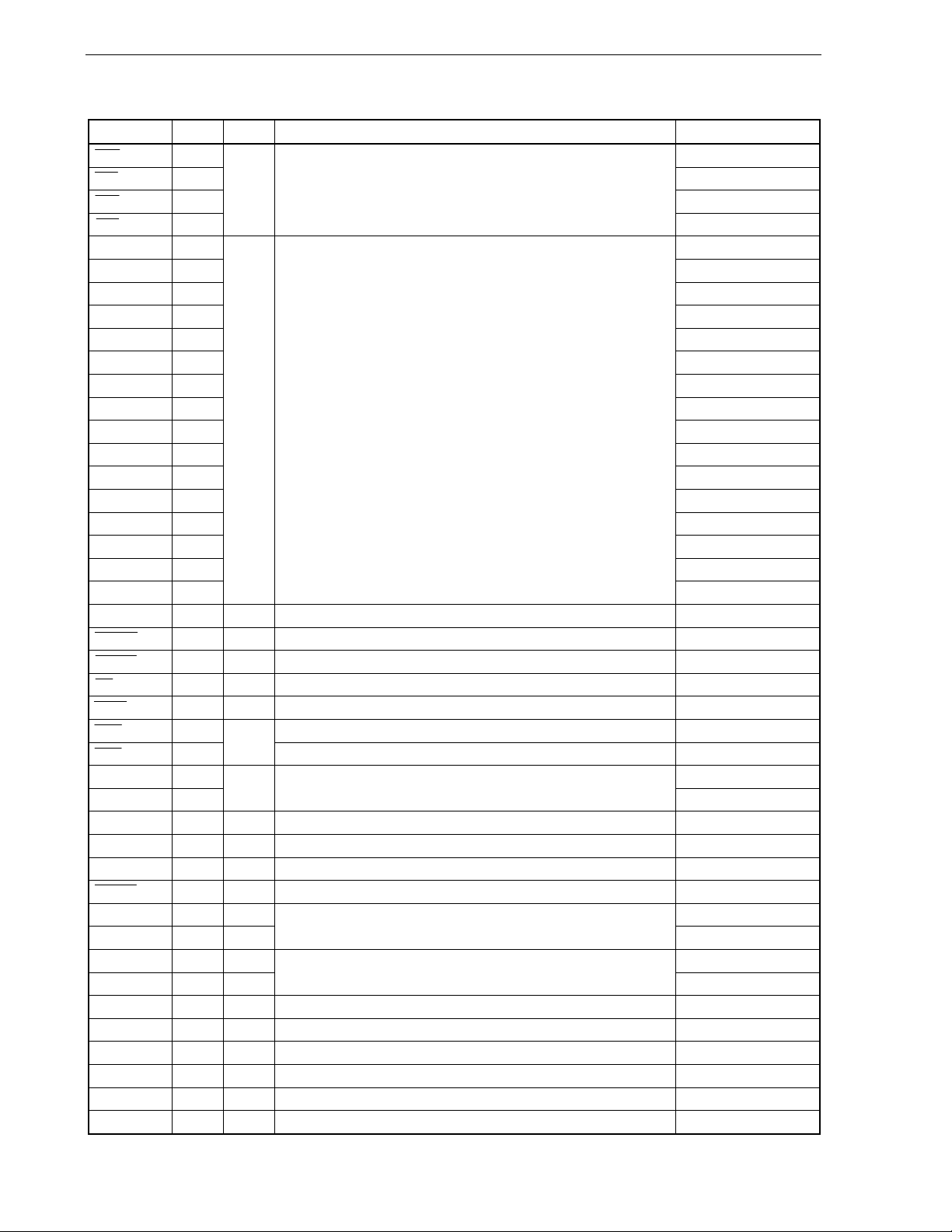
CHAPTER 2 PIN FUNCTIONS
Table 2-3. List of Pins (Non-Port Pins) (4/4)
Pin Name Pin No. I/O Function Alternate Function
CS0 81 PCS0
CS1 82 PCS1
CS2 83 PCS2
CS3 84
AD0 105 PDL0
AD1 106 PDL1
AD2 107 PDL2
AD3 108 PDL3
AD4 109 PDL4
AD5 110 PDL5/FLMD1
AD6 111 PDL6
AD7 112 PDL7
AD8 113 PDL8
AD9 114 PDL9
AD10 115 PDL10
AD11 116 PDL11
AD12 117 PDL12
AD13 118 PDL13
AD14 119 PDL14
AD15 120
ASTB 101 Output Address strobe signal output for external memory PCT6
HLDRQ 88 Input Bus hold request input PCM3
HLDAK 87 Output Bus hold acknowledge output PCM2
RD 99 Output Read strobe signal output for external memory PCT4
WAIT 85 Input External wait input PCM0
WR0 95 Write strobe for external memory (lower 8 bits) PCT0
WR1 96
FLMD0 8
FLMD1 110
CLKOUT 86 Output Internal system clock output PCM1
PCL 74 Output Clock output (timing output of X1 input clock and subclock) P913/INTP4
REGC 10 − Regulator output stabilizing capacitor connection
RESET 14 Input System reset input
X1 12 Input
X2 13
XT1 15 Input
XT2 16
VDD 9 − Positive power supply pin for internal circuitry
VSS 11 − Ground potential for internal circuitry
BVDD 104 − Positive power supply pin for bus interface and alternate-function ports
BVSS 103 − Ground potential for bus interface and alternate-function ports
EVDD 34 − Positive power supply pin for external circuitry (same potential as VDD)
EVSS 33 − Ground potential for external circuitry (same potential as VSS)
Output Chip select signal output
I/O Address/data bus for external memory
Output
Write strove for external memory (higher 8 bits) PCT1
Input Flash programming mode setting pins
Main clock resonator connection
−
Subclock resonator connection
−
PCS3
PDL15
−
PDL5/AD5
−
−
−
−
−
−
−
−
−
−
−
−
34
User’s Manual U17717EJ3V0UD
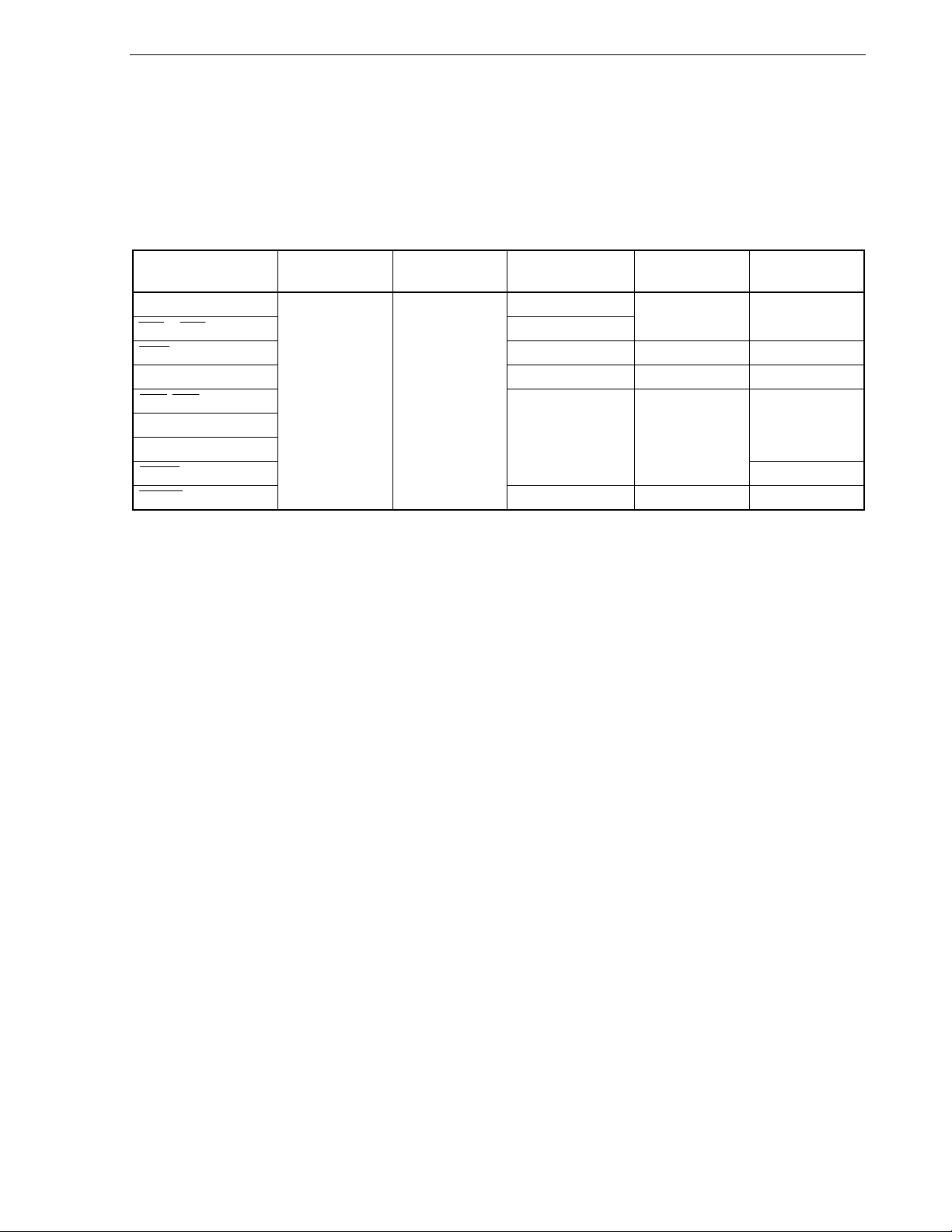
CHAPTER 2 PIN FUNCTIONS
2.2 Pin Status
The V850ES/HJ2 has an external bus interface function that enables connection of external memories, such as
ROM and RAM, and I/O.
Table 2-4 shows the operating status of each external bus interface pin in each operation mode.
Table 2-4. Pin Operating Status in Each Operation Mode
Bus Control Pin Reset HALT Mode and
Note 1
AD0 to AD15 Hi-Z
CS0 to CS3 H
WAIT − − −
CLKOUT L Operating Operating
WR0, WR1
RD
ASTB
HLDAK
HLDRQ
Hi-Z
Operating
DMA Transfer
IDLE1, IDLE2, and
STOP Modes
H H
− − Operating
Idle State
Notes 1. The bus control pins function alternately as port pins and are initialized to the input mode (port mode).
2. Pin status in the idle state that is inserted after the T3 state.
Remark Hi-Z: High impedance
Held: The state during the immediately preceding external bus cycle is held.
L: Low-level output
H: High-level output
−: Input without sampling (not acknowledged)
Note 2
Held Hi-Z
Bus Hold
Hi-Z
L
User’s Manual U17717EJ3V0UD
35

CHAPTER 2 PIN FUNCTIONS
2.3 Description of Pin Functions
(1) P00 to P06 (port 0) … 3-state I/O
P00 to P06 function as a 7-bit I/O port that can be set to input or output in 1-bit units.
Besides functioning as an I/O port, these pins operate as NMI input, external interrupt request signal input,
timer/counter I/O, external trigger of the A/D converter, and debug reset input.
This port can be set in the port mode or control mode in 1-bit units. The valid edge of each pin is specified by
the INTR0 and INTF0 registers.
An on-chip pull-up resistor can be connected to P00 to P06 by using pull-up resistor option register 0 (PU0).
(a) Port mode
P00 to P06 can be set in the input or output mode in 1-bit units, by using port mode register 0 (PM0).
(b) Control mode
(i) NMI (Non-maskable interrupt request) … input
This pin inputs a non-maskable interrupt request.
(ii) INTP0 to INTP3 (External interrupt request) … input
These pins input external interrupt request signals.
(iii) TIP30, TIP31 (Timer input) … input
These pins input an external count clock to timer P3 (TMP3).
(iv) TOP30, TOP31 (Timer output) … output
These pins output a pulse signal from timer P3 (TMP3).
(v) ADTRG (A/D trigger input) … input
This pin inputs an external trigger to the A/D converter. It is controlled by using A/D converter mode
register 0 (ADA0M0).
(vi) DRST (Debug reset) … input
This pin inputs a debug reset signal, a negative-logic signal that asynchronously initializes the debug
control unit (DCU). To deassert this signal, reset or invalidate the DCU. Deassert this signal when
the debug function is not used.
For details, see CHAPTER 26 ON-CHIP DEBUG FUNCTION.
36
User’s Manual U17717EJ3V0UD

CHAPTER 2 PIN FUNCTIONS
(2) P10, P11 (port 1) … 3-state I/O
P10 and P11 function as a 2-bit I/O port that can be set to input or output in 1-bit units.
Besides functioning as an I/O port, these pins operate as external interrupt request signal input in the control
mode. This port can be set in the port mode or control mode in 1-bit units. The valid edge of each pin is
specified by INTR1 and INTF1 registers.
An on-chip pull-up resistor can be connected to P10 and P11 by using pull-up resistor option register 1 (PU1).
(a) Port mode
P10 and P11 can be set in the input or output mode in 1-bit units, by using port mode register 1 (PM1).
(b) Control mode
(i) INTP9, INTP10 (External interrupt request) … input
These pins input an external interrupt request signal.
(3) P30 to P39 (port 3) … 3-state I/O
P30 to P39 function as a 10-bit I/O port that can be set to input or output in 1-bit units.
Besides functioning as an I/O port, these pins operate as external interrupt request signal input, serial interface
I/O, and timer/counter I/O. This port can be set in the port mode or control mode in 1-bit units. The valid edge
of each pin is specified by the INTR3 and INTF3 registers.
An on-chip pull-up resistor can be connected to P30 to P39 by using pull-up resistor option register 3 (PU3).
(a) Port mode
P30 to P39 can be set in the input or output mode in 1-bit units, by using port mode register 3 (PM3).
(b) Control mode
(i) RXDA0, RXDA2 (Receive data) … input
These pins input the serial receive data of UARTA0 and UARTA2.
(ii) TXDA0, TXDA2 (Transmit data) … output
These pins output the serial transmit data of UARTA0 and UARTA2.
(iii) ASCKA0 (Asynchronous serial clock) … input
This is an input pin for UARTA0.
(iv) INTP7, INTP8 (External interrupt request) … input
These pins input an external interrupt request signal.
(v) TIP00, TIP01, TIP10, TIP11 (Timer input) … input
These are input pins for timers P0 and P1 (TMP0 and TMP1).
(vi) TOP00, TOP01, TOP10, TOP11 (Timer output) … output
These are output pins for timers P0 and P1 (TMP0 and TMP1).
User’s Manual U17717EJ3V0UD
37

CHAPTER 2 PIN FUNCTIONS
(4) P40 to P42 (port 4) … 3-state I/O
P40 to P42 function as a 3-bit I/O port that can be set to input or output in 1-bit units.
Besides functioning as an I/O port, these pins operate as serial interface I/O. This port can be set in the port
mode or control mode in 1-bit units.
An on-chip pull-up resistor can be connected to P40 to P42 by using pull-up resistor option register 4 (PU4).
(a) Port mode
P40 to P42 can be set in the input or output mode in 1-bit units, by using port mode register 4 (PM4).
(b) Control mode
(i) SIB0 (Serial input) … input
This pin inputs the serial receive data of CSIB0.
(ii) SOB0 (Serial output) … output
This pin outputs the serial transmit data of CSIB0.
(iii) SCKB0 (serial clock) … 3-state I/O
This pin inputs/outputs the serial clock of CSIB0.
(5) P50 to P55 (Port 5) … 3-state I/O
P50 to P55 function as a 6-bit I/O port that can be set to input or output in 1-bit units.
Besides functioning as an I/O port, these pins operate as timer/counter I/O, debug function I/O, and key
interrupt input. This port can be set in the port mode or control mode in 1-bit units.
An on-chip pull-up resistor can be connected to P50 to P55 by using pull-up resistor option register 5 (PU5).
(a) Port mode
P50 to P55 can be set in the input or output mode in 1-bit units, by using port mode register 5 (PM5).
(b) Control mode
(i) KR0 to KR5 (Key return) … input
These pins input a key interrupt. Their operation is specified by using the key return mode register
(KRM) in the input port mode.
(ii) TIQ00, TIQ01, TIQ02, TIQ03 (Timer input) … input
These are input pins for timer Q0 (TMQ0).
(iii) TOQ00, TOQ01, TOQ02, TOQ03 (Timer output) … output
These are output pins for timer Q0 (TMQ0).
(iv) DDI (Debug data input) … input
This pin inputs debug data to the debug control unit (DCU).
For details, see CHAPTER 26 ON-CHIP DEBUG FUNCTION.
(v) DDO (Debug data output) … output
This pin outputs debug data from the DCU.
For details, see CHAPTER 26 ON-CHIP DEBUG FUNCTION.
38
User’s Manual U17717EJ3V0UD

CHAPTER 2 PIN FUNCTIONS
(iv) DCK (Debug clock input) … input
This pin inputs a debug clock to the DCU.
For details, see CHAPTER 26 ON-CHIP DEBUG FUNCTION.
(vii) DMS (Debug mode select) … input
This pin selects the debug mode of the DCU.
For details, see CHAPTER 26 ON-CHIP DEBUG FUNCTION.
(6) P60 to P615 (Port 6) … 3-state I/O
P60 to P615 function as a 16-bit I/O port that can be set to input or output in 1-bit units.
Besides functioning as an I/O port, these pins operate as external interrupt request signal input and
timer/counter I/O. P60 to P62 can be set in the port mode or control mode in 1-bit units. The valid edge of
P60 to P615 is specified by INTR6L and INTF6L registers.
An on-chip pull-up resistor can be connected to P60 to P615 by using pull-up resistor option register 6 (PU6).
(a) Port mode
P60 to P615 can be set in the input or output mode in 1-bit units, by using port mode register 6 (PM6).
(b) Control mode
(i) INTP11 to INTP13 (External interrupt request) … input
These pins input an external interrupt request signal.
(ii) TIQ20, TIQ21, TIQ22, TIQ23 (Timer input) … input
These are input pins for timer Q2 (TMQ2).
(iii) TOQ20, TOQ21, TOQ22, TOQ23 (Timer output) … output
These are output pins for timer Q2 (TMQ2).
(7) P70 to P715 (port 7) … 3-state I/O
P70 to P715 function as a 16-bit I/O port that can be set to input or output in 1-bit units.
Besides functioning as an I/O port, these pins operate as analog input to the A/D converter in the control mode.
When using the analog input pins, however, set this port in the input mode. At this time, do not read the port.
(a) Port mode
P70 to P715 can be set in the input or output mode in 1-bit units, by using port mode registers 7L and 7H
(PM7L and PM7H).
(b) Control mode
P70 to P715 function alternately as the ANI0 to ANI15 pins.
(i) ANI0 to ANI15 (Analog input 0 to 15) … input
These pins input an analog signal to the A/D converter.
User’s Manual U17717EJ3V0UD
39

CHAPTER 2 PIN FUNCTIONS
(8) P80 and P81 (port 8) … 3-state I/O
P80 and P81 function as a 2-bit I/O port that can be set to input or output in 1-bit units.
Besides functioning as an I/O port, these pins operate as external interrupt request signal input, and serial
interface I/O
Note
. P80 and P81 can be set in the port mode or control mode in 1-bit units. The valid edge of
each pin is specified by INTR8 and INTF8 registers.
An on-chip pull-up resistor can be connected to P80 and P81 by using pull-up resistor option register 8 (PU8).
(a) Port mode
P80 and P81 can be set in the input or output mode in 1-bit units, by using port mode register 8 (PM8).
(b) Control mode
(i) INTP14 (External interrupt request) … input
This pin inputs an external interrupt request signal.
(ii) RXDA3 (Receive data)
Note
… input
This pin inputs the serial receive data of UARTA3.
(iii) TXDA3 (Transmit data)
Note
… output
This pin outputs the serial transmit data of UARTA3.
Note
μ
PD70F3711 and 70F3712 only
(9) P90 to P915 (port 9) … 3-state I/O
P90 to P915 function as a 16-bit I/O port that can be set to input or output in 1-bit units.
Besides functioning as an I/O port, these pins operate as serial interface I/O, timer/counter I/O, clock output,
external interrupt request signal input, and key interrupt input. This port can be set in the port mode or control
mode in 1-bit units. The valid edge of P913 to P915 is specified by INTR9H and INTF9H registers.
An on-chip pull-up resistor can be connected to P90 to P915 by using pull-up resistor option register 9 (PU9).
(a) Port mode
P90 to P915 can be set in the input or output mode in 1-bit units, by using port mode register 9 (PM9).
(b) Control mode
(i) SIB1, SIB2 (Serial input) … input
These pins input the serial receive data of CSIB1 and CSIB2.
(ii) SOB1, SOB2 (Serial output) … output
These pins output the serial transmit data of CSIB1 and CSIB2.
(iii) SCKB1, SCKB2 (Serial clock) … 3-state I/O
These pins input/output the serial clock of CSIB1 and CSIB2.
(iv) RXDA1 (Receive data) … input
This pin inputs the serial receive data of UARTA1.
40
User’s Manual U17717EJ3V0UD

CHAPTER 2 PIN FUNCTIONS
(v) TXDA1 (Transmit data) … output
This pin outputs the serial transmit data of UARTA1.
(vi) TIP20, TIP21 (Timer input) … input
These are input pins for timer P2 (TMP2).
(vii) TOP20, TOP21 (Timer output) … output
These are output pins for timer P2 (TMP2).
(viii) TIQ10, TIQ11, TIQ12, TIQ13 (Timer input) … input
These are input pins for timer Q1 (TMQ1).
(ix) TOQ10, TOQ11, TOQ12, TOQ13 (Timer output) … output
These are output pins for timer Q1 (TMQ1).
(x) PCL (Clock output) … output
This pin outputs a clock.
(xi) INTP4 to INTP6 (External interrupt request) … input
These pins input an external interrupt request signal.
(xii) KR6, KR7 (Key return) … input
These pins input a key interrupt. Their operation is specified by the key return mode register (KRM) in
the input port mode.
(10) P120 to P127 (Port 12) … 3-state I/O
P120 to P127 function as an 8-bit I/O port that can be set to input or output in 1-bit units.
Besides functioning as an I/O port, these pins operate as the analog input pins of the A/D converter in the
control mode. When using this port as analog input pins, however, set the port in the input mode. At this time,
do not read the port.
(a) Port mode
P120 to P127 can be set in the input or output mode in 1-bit units, by using port mode register 12 (PM12).
(b) Control mode
P120 to P127 function alternately as the ANI16 to ANI23 pins.
(i) ANI16 to ANI23 (Analog input 16 to 23) … input
These pins input an analog signal to the A/D converter.
(11) PCD0 to PCD3 (port CD) … 3-state I/O
PCD0 to PCD3 function as a 4-bit I/O port that can be set to input or output in 1-bit units.
(a) Port mode
PCD0 to PCD3 can be set in the input or output mode in 1-bit units, by using port mode register CD
(PMCD).
User’s Manual U17717EJ3V0UD
41

CHAPTER 2 PIN FUNCTIONS
(12) PCM0 to PCM5 (port CM) … 3-state I/O
PCM0 to PCM5 function as a 6-bit I/O port that can be set to input or output in 1-bit units.
Besides functioning as an I/O port, these pins operate as bus hold control signal I/O, bus clock output, and a
control signal that inserts a wait cycle in the bus cycle (WAIT), in the control mode.
(a) Port mode
PCM0 to PCM5 can be set in the input or output mode in 1-bit units, by using port mode register CM
(PMCM).
(b) Control mode
(i) HLDAK (Hold acknowledge) … output
This pin outputs an acknowledge signal that indicates that the V850ES/HJ2 has placed the address
bus, data bus, and control bus in a high-impedance state in response to a bus hold request.
While this signal is active, the address bus, data bus, and control bus go into a high-impedance state.
(ii) HLDRQ (Hold request) … input
An external device uses this input pin to request the V850ES/HJ2 to release the address bus, data
bus, and control bus. A signal can be input to this pin asynchronously to CLKOUT. When this pin is
asserted, the V850ES/HJ2 places the address bus, data bus, and control bus in a high-impedance
state after completion of a bus cycle under execution, if any, or immediately if no such bus cycle is
under execution. The V850ES/HJ2 then asserts the HLDAK signal and releases the buses.
(iii) CLKOUT (Clock output) … output
This pin outputs an internally generated bus clock.
(iv) WAIT (Wait) … input
This is a control signal input pin that inserts a data wait state in the bus cycle. A signal can be input to
this pin asynchronously to the CLKOUT signal. The signal input to this pin is sampled at the falling
edge of the CLKOUT signal in the T2 and TW states of the bus cycle. No wait state may be inserted
if the setup/hold time of the sampling timing is not satisfied.
The wait function is set to on or off by port mode control register CM (PMCCM).
(13) PCS0 to PCS7 (port CS) … 3-state I/O
PCS0 to PCS7 function as an 8-bit I/O port that can be set to input or output in 1-bit units.
Besides functioning as an I/O port, these pins operate as chip select signal output in the control mode.
(a) Port mode
PCS0 to PCS7 can be set in the input or output mode in 1-bit units, by using port mode register CS
(PMCS).
(b) Control mode
(i) CS0 to CS3 (Chip select input) … output
These pins output a chip select signal to external memory and external peripheral I/O.
The CSn signal is assigned to memory block n (n = 0 to 3).
This signal is asserted while a bus cycle for accessing the corresponding memory block is being
executed.
This signal is deasserted in the idle state (TI).
42
User’s Manual U17717EJ3V0UD

CHAPTER 2 PIN FUNCTIONS
(14) PCT0 to PCT7 (port CT) … 3-state I/O
PCT0 to PCT7 function as an 8-bit I/O port that can be set to input or output in 1-bit units.
Besides functioning as an I/O port, these pins operate as control signal output in the control mode when
memory is externally expanded.
(a) Port mode
PCT0 to PCT7 can be set in the input or output mode in 1-bit units, by using port mode register CT
(PMCT).
(b) Control mode
(i) WR0 (Lower byte write strobe) … output
This pin outputs the write strobe signal of the lower data of the external 16-bit data bus.
(ii) WR1 (Upper byte write strobe) … output
This pin outputs the write strobe signal of the higher data of the external 16-bit data bus.
(iii) RD (Read strobe) … output
This pin outputs the read strobe signal of the external 16-bit data bus.
(iv) ASTB (Address strobe) … output
This pin outputs the latch strobe signal of the external address bus. The signal output from this pin
goes low at the falling edge of the T1 state of the bus cycle, and goes high at the falling edge of the
T3 state. It goes high while the bus cycle is not active.
(15) PDL0 to PDL15 (port DL) … 3-state I/O
PDL0 to PDL15 function as a 16-bit I/O port that can be set to input or output in 1-bit units.
Besides functioning as an I/O port, these pins operate as a time-division address/data bus (AD0 to AD15)
when the memory is externally expanded.
PDL5/AD5 also functions as the FLMD1 pin when the flash memory is programmed (when a high level is input
to FLMD0). At this time, be sure to input a low level to the FLMD1 pin.
(a) Port mode
PDL0 to PDL15 can be set in the input or output mode in 1-bit units, by using port mode register DL
(PMDL).
(b) Control mode
(i) AD0 to AD15 (Address/Data Bus 0 to 15) … 3-state I/O
These are multiplexed address/data bus for external access.
(16) RESET (Reset) … input
RESET input is asynchronous input. When a signal with a fixed low level width is input to the RESET pin
regardless of the operating clock, the system is reset, taking precedence over all the other operations.
This pin is used to release the standby mode (HALT, IDLE, or STOP), as well as for normal initialization/start.
User’s Manual U17717EJ3V0UD
43

CHAPTER 2 PIN FUNCTIONS
(17) X1, X2 (Crystal for main clock)
These pins are used to connect the resonator that generates the system clock.
(18) XT1, XT2 (Crystal for subclock)
These pins are used to connect the resonator that generates the subclock.
(19) AV
SS (Ground for analog)
This is a ground pin for the A/D converter and alternate-function ports.
(20) AV
REF0 (Analog reference voltage) … input
This pin supplies positive analog power to the A/D converter and alternate-function ports.
It also supplies a reference voltage to the A/D converter.
(21) EV
DD (Power supply for port)
This pin supplies positive power to the I/O ports and alternate-function pins.
(22) EV
SS (Ground for port)
This is a ground pin for the I/O ports and alternate-function pins.
(23) V
DD (Power supply)
This pin supplies positive power. Connect all the V
DD pins to a positive power supply.
(24) VSS (Ground)
This is a ground pin. Connect all the V
SS pins to ground.
(25) FLMD0 (Flash programming mode) … input
This is a signal input pin for flash memory programming mode.
Connect this pin to V
SS in the normal operation mode.
(26) BV
DD (Power supply for port)
This pin supplies positive power to the I/O ports and alternate-function pins.
(27) BV
SS (Ground for port)
This is a ground pin for the I/O ports and alternate-function pins.
(28) REGC (Regulator control) … input
This pin connects a capacitor for the regulator.
44
User’s Manual U17717EJ3V0UD

CHAPTER 2 PIN FUNCTIONS
2.4 Pin I/O Circuit Types and Recommended Connection of Unused Pins
Pin Pin No.
I/O Circuit
Type
P00/TIP31/TOP31 6
5-W
P01/TIP30/TOP30 7
Input: Independently connect to EV
Output: Leave open
P02/NMI 17
P03/INTP0/ADTRG 18
P04/INTP1 19
P05/INTP2/DRST 20 5-AF
Input: Independently connect to EV
Output: Leave open
Recommended Connection
(1/3)
DD or EVSS via a resistor
SS
P06/INTP3 21 5-W
Input: Independently connect to EV
Output: Leave open
P10/INTP9 3
5-W
P11/INTP10 4
P30/TXDA0 25 5-A
P31/RXDA0/INTP7 26
5-W
Input: Independently connect to EV
Output: Leave open
Input: Independently connect to EV
Output: Leave open
P32/ASCKA0/TIP00/TOP00/TOP01 27
P33/TIP01/TOP01 28
P34/TIP10/TOP10 29
P35/TIP11/TOP11 30
P36 31
5-A
P37 32
P38/TXDA2 35
P39/RXDA2/INTP8 36 5-W
P40/SIB0 22 5-W
P41/SOB0 23 5-A
Input: Independently connect to EV
Output: Leave open
P42/SCKB0 24 5-W
P50/KR0/TIQ01/TOQ01 37
5-W
P51/KR1/TIQ02/TOQ02 38
Input: Independently connect to EV
Output: Leave open
P52/KR2/TIQ03/TOQ03/DDI 39
P53/KR3/TIQ00/TOQ00/DDO 40
P54/KR4/DCK 41
P55/KR5/DMS 42
P60/INTP11 43
5-W
P61/INTP12 44
P62/INTP13 45
DD or EVSS via a resistor
DD or EVSS via a resistor
DD or EVSS via a resistor
DD or EVSS via a resistor
DD or EVSS via a resistor
User’s Manual U17717EJ3V0UD
45

CHAPTER 2 PIN FUNCTIONS
Pin Pin No.
I/O Circuit
Recommended Connection
Type
P63 46
5-A
P64 47
Input: Independently connect to EV
Output: Leave open
P65 48
P66 49
P67 50
P68 51
P69 52
P610/TIQ20/TOQ20 53
5-W
P611/TIQ21/TOQ21 54
P612/TIQ22/TOQ22 55
P613/TIQ23/TOQ23 56
P614 57
5-A
P615 58
P70/ANI0 to P715/ANI15 144 to 129 11-G
Input: Independently connect to AV
Output: Leave open
P80/RXDA3
P81/TXDA3
P90/KR6/TXDA1 61
Note
/INTP14 59 5-W
Note
60 5-A
5-W
P91/KR7/RXDA1 62
Input: Independently connect to EV
Output: Leave open
Input: Independently connect to EV
Output: Leave open
P92/TIQ11/TOQ11 63
P93/TIQ12/TOQ12 64
P94/TIQ13/TOQ13 65
P95/TIQ10/TOQ10 66
P96/TIP21/TOP21 67
P97/SIB1/TIP20/TOP20 68
P98/SOB1 69 5-A
P99/SCKB1 70
5-W
P910/SIB2 71
P911/SOB2 72 5-A
P912/SCKB2 73 5-W
P913/INTP4/PCL 74
5-W
P914/INTP5 75
Input: Independently connect to EV
Output: Leave open
P915/INTP6 76
P120/ANI16 to P127/ANI23 128 to 121 11-G
Input: Independently connect to AV
Output: Leave open
PCD0 to PCD3 77 to 80 5
Input: Independently connect to BV
Output: Leave open
Note
μ
PD70F3711, 70F3712 only
(2/3)
DD or EVSS via a resistor
REF0 or AVSS via a resistor
DD or EVSS via a resistor
DD or EVSS via a resistor
DD or EVSS via a resistor
REF0 or AVSS via a resistor
DD or BVSS via a resistor
46
User’s Manual U17717EJ3V0UD

CHAPTER 2 PIN FUNCTIONS
Pin Pin No. I/O Circuit
Recommended Connection
Type
PCM0/WAIT 85
PCM1/CLKOUT 86
5 Input: Independently connect to BV
Output: Leave open
DD or BVSS via a resistor
PCM2/HLDAK 87
PCM3/HLDRQ 88
PCM4 89
PCM5 90
PCS0/CS0 to PCS3/CS3 81 to 84
PCS4 to PCS7 91 to 94
PCT0/WR0 95
PCT1/WR1 96
5 Input: Independently connect to BV
Output: Leave open
5 Input: Independently connect to BV
Output: Leave open
DD or BVSS via a resistor
DD or BVSS via a resistor
PCT2 97
PCT3 98
PCT4/RD 99
PCT5 100
PCT6/ASTB 101
PCT7 102
PDL0/AD0 to PDL4/AD4 105 to 109
PDL5/AD5/FLMD1 110
5 Input: Independently connect to BV
Output: Leave open
DD or BVSS via a resistor
PDL6/AD6 to PDL15/AD15 111 to 120
AVREF0 1
AVSS 2
Note
FLMD0
8
REGC 10
RESET 14 2
X1 12
X2 13
Directly connect to VDD
−
− −
Directly connect to VSS
−
− −
− −
− −
−
XT1 15 16 Connect to VSS via a resistor
XT2 16 16 Leave open
VDD 9
VSS 11
BVDD 104
BVSS 103
EVDD 34
EVSS 33
− −
− −
− −
− −
− −
− −
Note If noise that exceeds the noise elimination width is input to the RESET pin during self programming, the
flash on-board mode may be entered depending on the capacitance charge end timing when a capacitor is
connected to the FLMD0 pin. Therefore, do not connect a capacitor to the FLMD0 pin.
(3/3)
User’s Manual U17717EJ3V0UD
47
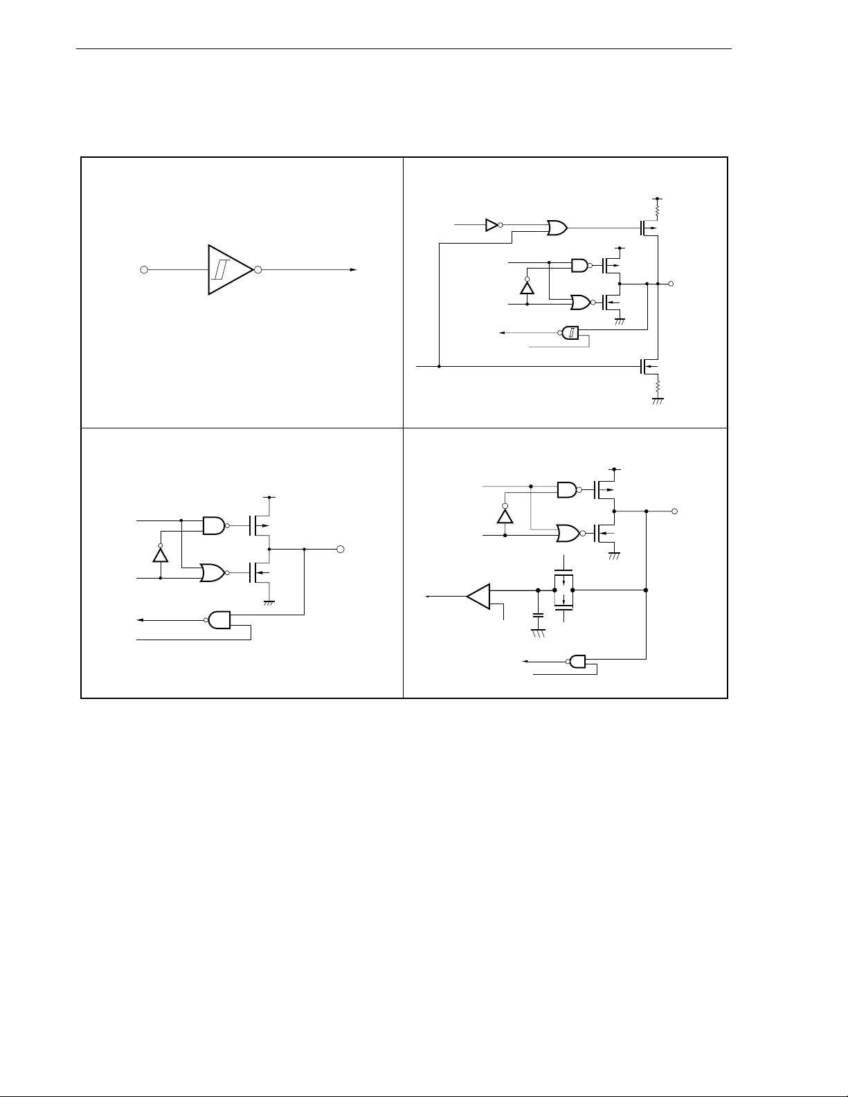
CHAPTER 2 PIN FUNCTIONS
2.5 Pin I/O Circuits
Figure 2-1. Pin I/O Circuit Types (1/2)
Type 2 Type 5-AF
Pull-up
enable
IN
Schmitt-triggered input with hysteresis characteristics
Pull-down
enable
Data
Output
disable
Input enable
V
DD
P-ch
N
-ch
V
P-ch
N
-ch
DD
IN/OUT
Type 5 Type 11-G
V
DD
Data
Output
disable
Input
enable
P-ch
N-ch
IN/OUT
Output
disable
Comparator
(Threshold voltage)
Data
+
_
V
REF
Input enable
AV
AV
REF0
P-ch
IN/OUT
N-ch
AV
P-ch
SS
N-ch
SS
48
User’s Manual U17717EJ3V0UD

CHAPTER 2 PIN FUNCTIONS
Figure 2-1. Pin I/O Circuit Types (2/2)
Type 5-A
Pull-up
enable
Data
Output
disable
Input
enable
Type 5-W
Pull-up
enable
Data
Output
disable
V
DD
P-ch
N-ch
DD
V
P-ch
N
-ch
Type 16
V
DD
Feedback cut-off
P-ch
V
DD
P-ch
IN/OUT
XT1 XT2
IN/OUT
P-ch
Input
enable
Remark Read V
DD as EVDD or BVDD. Also, read VSS as EVSS or BVSS.
2.6 Cautions
Note that the following pin may temporarily output an undefined level, even during reset upon power application.
P53/KR3/TIQ00/TOQ00/DDO pin
User’s Manual U17717EJ3V0UD
49

CHAPTER 3 CPU FUNCTION
The CPU of the V850ES/HJ2 is based on RISC architecture and executes almost all instructions with one clock by
using a 5-stage pipeline.
3.1 Features
Minimum instruction execution time: 50 ns (at 20 MHz operation)
Memory space Program (physical address) space: 64 MB linear
Data (logical address) space: 4 GB linear
General-purpose registers: 32 bits × 32 registers
Internal 32-bit architecture
5-stage pipeline control
Multiplication/division instruction
Saturation operation instruction
32-bit shift instruction: 1 clock
Load/store instruction with long/short format
Four types of bit manipulation instructions
• SET1
• CLR1
• NOT1
• TST1
50
User’s Manual U17717EJ3V0UD

CHAPTER 3 CPU FUNCTION
3.2 CPU Register Set
The registers of the V850ES/HJ2 can be classified into two types: general-purpose program registers and
dedicated system registers. All the registers are 32 bits wide.
For details, refer to the V850ES Architecture User’s Manual.
(1) Program register set
(2) System register set
31 0 31 0
r0
r1
r2
r3
r4
r5
r6
r7
r8
r9
r10
r11
r12
r13
r14
r15
r16
r17
r18
r19
r20
r21
r22
r23
r24
r25
r26
r27
r28
r29
r30
r31
(Zero register)
(Assembler-reserved register)
(Stack pointer (SP))
(Global pointer (GP))
(Text pointer (TP))
(Element pointer (EP))
(Link pointer (LP))
EIPC
EIPSW
FEPC
FEPSW
ECR
PSW
CTPC
CTPSW
DBPC
DBPSW
CTBP
(Interrupt status saving register)
(Interrupt status saving register)
(NMI status saving register)
(NMI status saving register)
(Interrupt source register)
(Program status word)
(CALLT execution status saving register)
(CALLT execution status saving register)
(Exception/debug trap status saving register)
(Exception/debug trap status saving register)
(CALLT base pointer)
31 0
PC
(Program counter)
User’s Manual U17717EJ3V0UD
51
CHAPTER 3 CPU FUNCTION
3.2.1 Program register set
The program registers include general-purpose registers and a program counter.
(1) General-purpose registers (r0 to r31)
Thirty-two general-purpose registers, r0 to r31, are available. Any of these registers can be used to store a
data variable or an address variable.
However, r0 and r30 are implicitly used by instructions and care must be exercised when these registers are
used. r0 always holds 0 and is used for an operation that uses 0 or addressing of offset 0. r30 is used by the
SLD and SST instructions as a base pointer when these instructions access the memory. r1, r3 to r5, and r31
are implicitly used by the assembler and C compiler. When using these registers, save their contents for
protection, and then restore the contents after using the registers. r2 is sometimes used by the real-time OS.
If the real-time OS does not use r2, it can be used as a register for variables.
Table 3-1. Program Registers
Name Usage Operation
r0 Zero register Always holds 0.
r1 Assembler-reserved register Used as working register to create 32-bit immediate data
r2 Register for address/data variable (if real-time OS does not use r2)
r3 Stack pointer Used to create a stack frame when a function is called
r4 Global pointer Used to access a global variable in the data area
r5 Text pointer Used as register that indicates the beginning of a text area (area
where program codes are located)
r6 to r29 Register for address/data variable
r30 Element pointer Used as base pointer to access memory
r31 Link pointer Used when the compiler calls a function
PC Program counter Holds the instruction address during program execution
Remark For furthers details on the r1, r3 to r5, and r31 that are used in the assembler and C compiler, refer
to the CA850 (C Compiler Package) Assembly Language User’s Manual.
(2) Program counter (PC)
The program counter holds the instruction address during program execution. The lower 26 bits of this register
are valid. Bits 31 to 26 are fixed to 0. A carry from bit 25 to 26 is ignored even if it occurs.
Bit 0 is fixed to 0. This means that execution cannot branch to an odd address.
31 26 25 1 0
PC
Fixed to 0 Instruction address during program execution
0
Default value
00000000H
52
User’s Manual U17717EJ3V0UD

CHAPTER 3 CPU FUNCTION
3.2.2 System register set
The system registers control the status of the CPU and hold interrupt information.
These registers can be read or written by using system register load/store instructions (LDSR and STSR), using
the system register numbers listed below.
Table 3-2. System Register Numbers
System Register Name
Register
Number
Note 1
Note 1
Note 1
Note 1
0 Interrupt status saving register (EIPC)
1 Interrupt status saving register (EIPSW)
2 NMI status saving register (FEPC)
3 NMI status saving register (FEPSW)
4 Interrupt source register (ECR)
5 Program status word (PSW)
6 to 15 Reserved for future function expansion (operation is not guaranteed if these
Operand Specification System
LDSR Instruction STSR Instruction
√ √
√ √
√ √
√ √
× √
√ √
× ×
registers are accessed)
16 CALLT execution status saving register (CTPC)
17 CALLT execution status saving register (CTPSW)
18 Exception/debug trap status saving register (DBPC) √
19 Exception/debug trap status saving register (DBPSW) √
20 CALLT base pointer (CTBP)
21 to 31 Reserved for future function expansion (operation is not guaranteed if these
√ √
√ √
Note 2
√
Note 2
√
√ √
× ×
Note 2
Note 2
registers are accessed)
Notes 1. Because only one set of these registers is available, the contents of these registers must be saved by
program if multiple interrupts are enabled.
2. These registers can be accessed only during the interval between the execution of the DBTRAP
instruction or illegal opcode and the DBRET instruction.
Caution Even if EIPC or FEPC, or bit 0 of CTPC is set to 1 by the LDSR instruction, bit 0 is ignored when
execution is returned to the main routine by the RETI instruction after interrupt servicing (this is
because bit 0 of the PC is fixed to 0). Set an even value to EIPC, FEPC, and CTPC (bit 0 = 0).
Remark √: Can be accessed
×: Access prohibited
User’s Manual U17717EJ3V0UD
53

CHAPTER 3 CPU FUNCTION
(1) Interrupt status saving registers (EIPC and EIPSW)
EIPC and EIPSW are used to save the status when an interrupt occurs.
If a software exception or a maskable interrupt occurs, the contents of the program counter (PC) are saved to
EIPC, and the contents of the program status word (PSW) are saved to EIPSW (these contents are saved to
the NMI status saving registers (FEPC and FEPSW) if a non-maskable interrupt occurs).
The address of the instruction next to the instruction under execution, except some instructions (see 16.8
Periods in Which Interrupts Are Not Acknowledged by CPU), is saved to EIPC when a software exception
or a maskable interrupt occurs.
The current contents of the PSW are saved to EIPSW.
Because only one set of interrupt status saving registers is available, the contents of these registers must be
saved by program when multiple interrupts are enabled.
Bits 31 to 26 of EIPC and bits 31 to 8 of EIPSW are reserved for future function expansion (these bits are
always fixed to 0).
The value of EIPC is restored to the PC and the value of EIPSW to the PSW by the RETI instruction.
EIPC
EIPSW
31 0
00
31 0
00
26 25
0 0 0 0
0 0 0 0 00 0 0 0 0 00 0 0 0 0 00 0 0 0 0
(Saved PC contents)
87
(Saved PSW
contents)
Default value
0xxxxxxxH
(x: Undefined)
Default value
000000xxH
(x: Undefined)
54
User’s Manual U17717EJ3V0UD
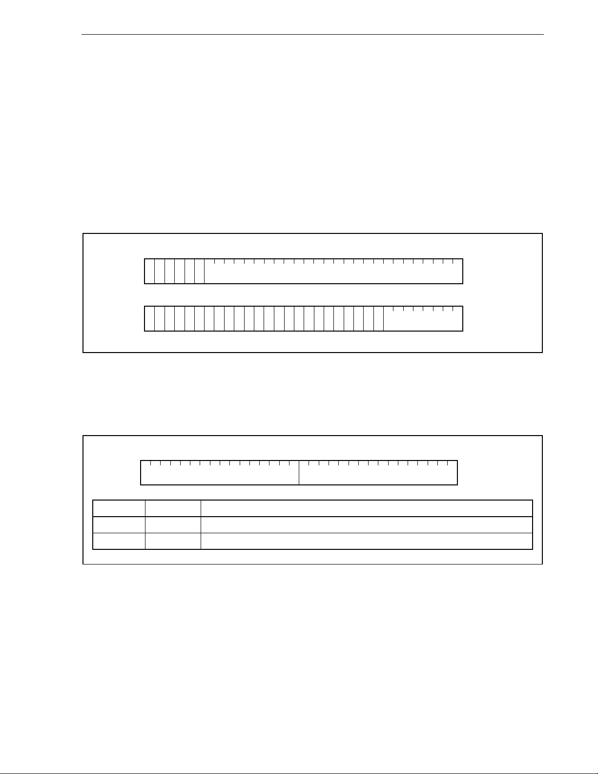
CHAPTER 3 CPU FUNCTION
(2) NMI status saving registers (FEPC and FEPSW)
FEPC and FEPSW are used to save the status when a non-maskable interrupt (NMI) occurs.
If an NMI occurs, the contents of the program counter (PC) are saved to FEPC, and those of the program
status word (PSW) are saved to FEPSW.
The address of the instruction next to the one of the instruction under execution, except some instructions, is
saved to FEPC when an NMI occurs.
The current contents of the PSW are saved to FEPSW.
Because only one set of NMI status saving registers is available, the contents of these registers must be saved
by program when multiple interrupts are enabled.
Bits 31 to 26 of FEPC and bits 31 to 8 of FEPSW are reserved for future function expansion (these bits are
always fixed to 0).
The value of FEPC is restored to the PC and the value of FEPSW to the PSW by the RETI instruction.
FEPC
FEPSW
31 0
00
31 0
00
26 25
0 0 0 0
0 0 0 0 00 0 0 0 0 00 0 0 0 0 00 0 0 0 0
(Saved PC contents)
87
(Saved PSW
contents)
Default value
0xxxxxxxH
(x: Undefined)
Default value
000000xxH
(x: Undefined)
(3) Interrupt source register (ECR)
The interrupt source register (ECR) holds the source of an exception or interrupt if an exception or interrupt
occurs. This register holds the exception code of each interrupt source. Because this register is a read-only
register, data cannot be written to this register using the LDSR instruction.
ECR
31 0
FECC EICC
16 15
Default value
00000000H
Bit position Bit name Meaning
31 to 16 FECC Exception code of non-maskable interrupt (NMI)
15 to 0 EICC Exception code of exception or maskable interrupt
User’s Manual U17717EJ3V0UD
55

CHAPTER 3 CPU FUNCTION
(4) Program status word (PSW)
The program status word (PSW) is a collection of flags that indicate the status of the program (result of
instruction execution) and the status of the CPU.
If the contents of a bit of this register are changed by using the LDSR instruction, the new contents are
validated immediately after completion of LDSR instruction execution. However if the ID flag is set to 1,
interrupt requests will not be acknowledged while the LDSR instruction is being executed.
Bits 31 to 8 of this register are reserved for future function expansion (these bits are fixed to 0).
PSW
31 0
RFU
87NP6EP5ID4
SAT3CY2OV
1
SZ
Default value
00000020H
Bit position Flag name Meaning
31 to 8 RFU Reserved field. Fixed to 0.
7 NP Indicates that a non-maskable interrupt (NMI) is being serviced. This bit is set to 1 when an
NMI request is acknowledged, disabling multiple interrupts.
0: NMI is not being serviced.
1: NMI is being serviced.
6 EP Indicates that an exception is being processed. This bit is set to 1 when an exception
occurs. Even if this bit is set, interrupt requests are acknowledged.
0: Exception is not being processed.
1: Exception is being processed.
5 ID Indicates whether a maskable interrupt can be acknowledged.
0: Interrupt enabled
1: Interrupt disabled
4 SAT
3 CY Indicates whether a carry or a borrow occurs as a result of an operation.
2 OV
1 S
0 Z Indicates whether the result of an operation is 0.
Note
Indicates that the result of a saturation operation has overflowed and is saturated. Because
this is a cumulative flag, it is set to 1 when the result of a saturation operation instruction is
saturated, and is not cleared to 0 even if the subsequent operation result is not saturated.
Use the LDSR instruction to clear this bit. This flag is neither set to 1 nor cleared to 0 by
execution of an arithmetic operation instruction.
0: Not saturated
1: Saturated
0: Carry or borrow does not occur.
1: Carry or borrow occurs.
Note
Indicates whether an overflow occurs during operation.
0: Overflow does not occur.
1: Overflow occurs.
Note
Indicates whether the result of an operation is negative.
0: The result is positive or 0.
1: The result is negative.
0: The result is not 0.
1: The result is 0.
(1/2)
Remark Also read Note on the next page.
56
User’s Manual U17717EJ3V0UD

CHAPTER 3 CPU FUNCTION
Note The result of the operation that has performed saturation processing is determined by the contents of the
OV and S flags. The SAT flag is set to 1 only when the OV flag is set to 1 when a saturation operation is
performed.
SAT OV S
Maximum positive value is exceeded 1 1 0 7FFFFFFFH
Maximum negative value is exceeded 1 1 1 80000000H
Positive (maximum value is not exceeded) 0
Negative (maximum value is not exceeded)
Holds value
before operation
Flag status Status of operation result
0
1
Result of operation of
saturation processing
Operation result itself
(5) CALLT execution status saving registers (CTPC and CTPSW)
CTPC and CTPSW are CALLT execution status saving registers.
When the CALLT instruction is executed, the contents of the program counter (PC) are saved to CTPC, and
those of the program status word (PSW) are saved to CTPSW.
The contents saved to CTPC are the address of the instruction next to CALLT.
The current contents of the PSW are saved to CTPSW.
Bits 31 to 26 of CTPC and bits 31 to 8 of CTPSW are reserved for future function expansion (fixed to 0).
CTPC
CTPSW
31 0
00
31 0
00
26 25
0 0 0 0
0 0 0 0 00 0 0 0 0 00 0 0 0 0 00 0 0 0 0
(Saved PC contents)
87
(Saved PSW
contents)
Default value
0xxxxxxxH
(x: Undefined)
Default value
000000xxH
(x: Undefined)
(2/2)
User’s Manual U17717EJ3V0UD
57
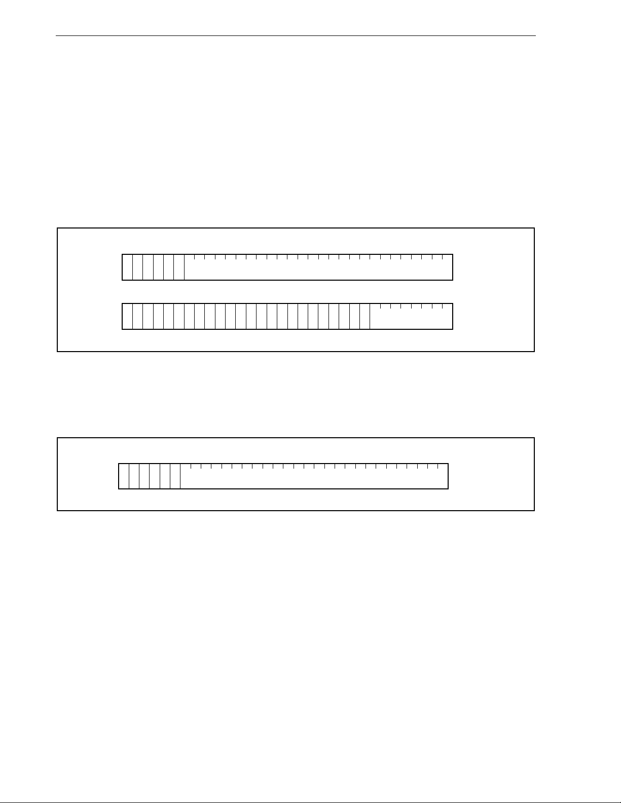
CHAPTER 3 CPU FUNCTION
(6) Exception/debug trap status saving registers (DBPC and DBPSW)
DBPC and DBPSW are exception/debug trap status registers.
If an exception trap or debug trap occurs, the contents of the program counter (PC) are saved to DBPC, and
those of the program status word (PSW) are saved to DBPSW.
The contents to be saved to DBPC are the address of the instruction next to the one that is being executed
when an exception trap or debug trap occurs.
The current contents of the PSW are saved to DBPSW.
This register can be read or written only during the interval between the execution of the DBTRAP instruction
or illegal opcode and the DBRET instruction.
Bits 31 to 26 of DBPC and bits 31 to 8 of DBPSW are reserved for future function expansion (fixed to 0).
The value of DBPC is restored to the PC and the value of DBPSW to the PSW by the DBRET instruction.
DBPC
DBPSW
31 0
00
31 0
00
26 25
0 0 0 0
0 0 0 0 00 0 0 0 0 00 0 0 0 0 00 0 0 0 0
(Saved PC contents)
87
(Saved PSW
contents)
Default value
0xxxxxxxH
(x: Undefined)
Default value
000000xxH
(x: Undefined)
(7) CALLT base pointer (CTBP)
The CALLT base pointer (CTBP) is used to specify a table address or generate a target address (bit 0 is fixed
to 0).
Bits 31 to 26 of this register are reserved for future function expansion (fixed to 0).
CTBP
31 0
00
26 25
0 0 0 0 0
(Base address)
Default value
0xxxxxxxH
(x: Undefined)
58
User’s Manual U17717EJ3V0UD
CHAPTER 3 CPU FUNCTION
3.3 Operation Modes
The V850ES/HJ2 has the following operation modes.
(1) Normal operation mode
In this mode, each pin related to the bus interface is set to the port mode after system reset has been released.
Execution branches to the reset entry address of the internal ROM, and then instruction processing is started.
(2) Flash memory programming mode
In this mode, the internal flash memory can be programmed by using a flash programmer.
(3) On-chip debug mode
The V850ES/HJ2 is provided with an on-chip debug function that employs the JTAG (Joint Test Action Group)
communication specifications.
For details, see CHAPTER 26 ON-CHIP DEBUG FUNCTION.
3.3.1 Specifying operation mode
Specify the operation mode by using the FLMD0 and FLMD1 pins.
In the normal mode, input a low level to the FLMD0 pin when reset is released.
In the flash memory programming mode, a high level is input to the FLMD0 pin from the flash programmer if a flash
programmer is connected, but it must be input from an external circuit in the self-programming mode.
Operation When Reset Is Released
FLMD0 FLMD1
Operation Mode After Reset
L
H L Flash memory programming mode
H H Setting prohibited
×
Normal operation mode
Remark L: Low-level input
H: High-level input
×: Don’t care
User’s Manual U17717EJ3V0UD
59

CHAPTER 3 CPU FUNCTION
3.4 Address Space
3.4.1 CPU address space
For instruction addressing, up to a combined total of 16 MB of external memory area and internal ROM area, plus
an internal RAM area, are supported in a linear address space (program space) of up to 64 MB. For operand
addressing (data access), up to 4 GB of a linear address space (data space) is supported. The 4 GB address space,
however, is viewed as 64 images of a 64 MB physical address space. This means that the same 64 MB physical
address space is accessed regardless of the value of bits 31 to 26.
Figure 3-1. Image on Address Space
Image 63
16 MB
Program space
Use-prohibited area
Internal RAM area
Use-prohibited area
External memory area
4 GB
64 MB
Image 1
Image 0
Data space
Peripheral I/O area
Internal RAM area
Use-prohibited area
64 MB
External memory area
Internal ROM area
(external memory area)
60
Internal ROM area
(external memory area)
User’s Manual U17717EJ3V0UD

CHAPTER 3 CPU FUNCTION
3.4.2 Wraparound of CPU address space
(1) Program space
Of the 32 bits of the PC (program counter), the higher 6 bits are fixed to 0 and only the lower 26 bits are valid.
The higher 6 bits ignore a carry or borrow from bit 25 to 26 during branch address calculation.
Therefore, the highest address of the program space, 03FFFFFFH, and the lowest address, 00000000H, are
contiguous addresses. That the highest address and the lowest address of the program space are contiguous
in this way is called wraparound.
Caution Because the 4 KB area of addresses 03FFF000H to 03FFFFFFH is an on-chip peripheral I/O
area, instructions cannot be fetched from this area. Therefore, do not execute an operation in
which the result of a branch address calculation affects this area.
00000001H
00000000H
03FFFFFFH
03FFFFFEH
Program space
(+) direction (−) direction
Program space
(2) Data space
The result of an operand address calculation operation that exceeds 32 bits is ignored.
Therefore, the highest address of the data space, FFFFFFFFH, and the lowest address, 00000000H, are
contiguous, and wraparound occurs at the boundary of these addresses.
00000001H
00000000H
FFFFFFFFH
Data space
(+) direction (−) direction
FFFFFFFEH
Data space
User’s Manual U17717EJ3V0UD
61

CHAPTER 3 CPU FUNCTION
3.4.3 Memory map
The areas shown below are reserved in the V850ES/HJ2.
Figure 3-2. Data Memory Map (Physical Addresses)
03FFFFFFH
(80 KB)
03FEC000H
03FEBFFFH
On-chip peripheral I/O area
(4 KB)
Internal RAM area
(60 KB)
Use prohibited
Use prohibited
Note 1
03FFFFFFH
03FFF000H
03FFEFFFH
03FF0000H
03FEFFFFH
03FEF000H
03FEEFFFH
00810000H
0080FFFFH
008000000H
007FFFFFFH
00410000H
0040FFFFH
00400000H
003FFFFFH
00210000H
0020FFFFH
00200000H
001FFFFFH
00000000H
Use prohibited
External memory area (64 KB)
Use prohibited
External memory area (64 KB)
Use prohibited
External memory area (64 KB)
(2 MB)
Use prohibited
External memory area (64 KB)
Internal ROM area
(1 MB)
Note 2
03FEC000H
001FFFFFH
00110000H
0010FFFFH
00100000H
000FFFFFH
00000000H
Notes 1. Use of addresses 03FEF000H to 03FEFFFFH is prohibited because these addresses are in the
same area as the on-chip peripheral I/O area.
2. Fetch access and read access to addresses 00000000H to 000FFFFFH is made to the internal ROM
area. However, data write access to these addresses is made to the external memory area.
62
User’s Manual U17717EJ3V0UD

CHAPTER 3 CPU FUNCTION
Figure 3-3. Program Memory Map
03FFFFFFH
03FFF000H
03FFEFFFH
Use prohibited
(program fetch prohibited area)
03FF0000H
03FEFFFFH
01000000H
00FFFFFFH
Internal RAM area (60 KB)
Use prohibited
(program fetch prohibited area)
External memory area
(14 MB)
Note
00200000H
001FFFFFH
00100000H
000FFFFFH
00000000H
Note For details, see 3.4.4 (2) Internal RAM area.
User’s Manual U17717EJ3V0UD
External memory area
(1 MB)
Internal ROM area
(1 MB)
63
3.4.4 Areas
(1) Internal ROM area
Up to 1 MB is reserved as an internal ROM area.
(a) Internal ROM (128 KB)
128 KB are allocated to addresses 0000000H to 001FFFFH in the
Accessing addresses 0020000H to 00FFFFFH is prohibited.
Figure 3-4. Internal ROM Area (128 KB)
CHAPTER 3 CPU FUNCTION
00FFFFFH
Access-prohibited
area
0020000H
001FFFFH
μ
PD70F3709.
(b) Internal ROM (256 KB)
256 KB are allocated to addresses 00000000H to 0003FFFFH in the
Accessing addresses 00040000H to 000FFFFFH is prohibited.
Internal ROM area
(128 KB)
0000000H
Figure 3-5. Internal ROM Area (256 KB)
00FFFFFH
Access-prohibited
area
0040000H
003FFFFH
Internal ROM area
(256 KB)
μ
PD70F3710.
64
0000000H
User’s Manual U17717EJ3V0UD

(c) Internal ROM (376 KB)
376 KB are allocated to addresses 00000000H to 0005DFFFH in the
Accessing addresses 0005E000H to 000FFFFFH is prohibited.
CHAPTER 3 CPU FUNCTION
Figure 3-6. Internal ROM Area (376 KB)
000FFFFFH
Access-prohibited
area
0005E000H
0005DFFFH
Internal ROM
(376 KB)
μ
PD70F3711.
(d) Internal ROM (512 KB)
512 KB are allocated to addresses 00000000H to 0007FFFFH in the
Accessing addresses 00080000H to 000FFFFFH is prohibited.
00000000H
Figure 3-7. Internal ROM Area (512 KB)
000FFFFFH
00080000H
0007FFFFH
00000000H
Access-prohibited
area
Internal ROM
(512 KB)
μ
PD70F3712.
User’s Manual U17717EJ3V0UD
65

(2) Internal RAM area
Up to 60 KB are reserved as the internal RAM area.
(a) Internal RAM (12 KB)
12 KB are allocated to addresses 03FFC000H to 03FFEFFFH in the following versions.
Accessing addresses 03FF0000H to 03FFBFFFH is prohibited.
•
μ
PD70F3709, 70F3710
Figure 3-8. Internal RAM Area (12 KB)
Physical address space Logical address space
CHAPTER 3 CPU FUNCTION
(b) Internal RAM (20 KB)
20 KB are allocated to addresses 03FFA000H to 03FFEFFFH in the following versions.
Accessing addresses 03FF0000H to 03FF9FFFH is prohibited.
•
μ
PD70F3711, 70F3712
03FFEFFFH
Internal RAM
03FFC000H
03FFBFFFH
Access-prohibited
area
03FF0000H
FFFFEFFFH
FFFFC000H
FFFFBFFFH
FFFF0000H
Figure 3-9. Internal RAM Area (20 KB)
Physical address space Logical address space
66
03FFEFFFH
03FFA000H
03FF9FFFH
03FF0000H
User’s Manual U17717EJ3V0UD
Internal RAM
Access-prohibited
area
FFFFEFFFH
FFFFA000H
FFFF9FFFH
FFFF0000H

CHAPTER 3 CPU FUNCTION
(3) On-chip peripheral I/O area
4 KB of addresses 03FFF000H to 03FFFFFFH are reserved as the on-chip peripheral I/O area.
Figure 3-10. On-Chip Peripheral I/O Area
Physical address space Logical address space
03FFFFFFH
On-chip peripheral I/O area
(4 KB)
03FFF000H
FFFFFFFFH
FFFFF000H
Peripheral I/O registers that have functions to specify the operation mode for and monitor the status of the on-
chip peripheral I/O are mapped to the on-chip peripheral I/O area. Program cannot be fetched from this area.
Cautions 1. When a register is accessed in word units, a word area is accessed twice in halfword
units in the order of lower area and higher area, with the lower 2 bits of the address
ignored.
2. If a register that can be accessed in byte units is accessed in halfword units, the higher 8
bits are undefined when the register is read, and data is written to the lower 8 bits.
3. Addresses not defined as registers are reserved for future expansion. The operation is
undefined and not guaranteed when these addresses are accessed.
(4) External memory area
256 KB are allocated as the external memory area. For details, see CHAPTER 5 BUS CONTROL
FUNCTION.
User’s Manual U17717EJ3V0UD
67

CHAPTER 3 CPU FUNCTION
3.4.5 Recommended use of address space
The architecture of the V850ES/HJ2 requires that a register that serves as a pointer be secured for address
generation when operand data in the data space is accessed. The address stored in this pointer ±32 KB can be
directly accessed by an instruction for operand data. Because the number of general-purpose registers that can be
used as a pointer is limited, however, by keeping the performance from dropping during address calculation when a
pointer value is changed, as many general-purpose registers as possible can be secured for variables, and the
program size can be reduced.
(1) Program space
Of the 32 bits of the PC (program counter), the higher 6 bits are fixed to 0, and only the lower 26 bits are valid.
Regarding the program space, therefore, a 64 MB space of contiguous addresses starting from 00000000H
unconditionally corresponds to the memory map.
To use the internal RAM area as the program space, access following addresses.
Caution If a branch instruction is at the upper limit of the internal RAM area, a prefetch operation
(invalid fetch) straddling the on-chip peripheral I/O area does not occur.
RAM Size Access Address
20 KB 03FFA000H to 03FFEFFFH
12 KB 03FFC000H to 03FFEFFFH
68
User’s Manual U17717EJ3V0UD

CHAPTER 3 CPU FUNCTION
(2) Data space
With the V850ES/HJ2, it seems that there are sixty-four 64 MB address spaces on the 4 GB CPU address
space. Therefore, the least significant bit (bit 25) of a 26-bit address is sign-extended to 32 bits and allocated
as an address.
(a) Application example of wraparound
If R = r0 (zero register) is specified for the LD/ST disp16 [R] instruction, a range of addresses 00000000H
±32 KB can be addressed by sign-extended disp16. All the resources, including the internal hardware, can
be addressed by one pointer.
The zero register (r0) is a register fixed to 0 by hardware, and practically eliminates the need for registers
dedicated to pointers.
Figure 3-11. Wraparound (
μ
PD70F3712)
0005FFFFH
00007FFFH
(R = )
00000000H
FFFFF000H
FFFFEFFFH
FFFFA000H
FFFF9FFFH
FFFF8000H
Internal ROM area
On-chip peripheral
I/O area
Internal RAM area
Access-prohibited
area
32 KB
4 KB
20 KB
8 KB
User’s Manual U17717EJ3V0UD
69
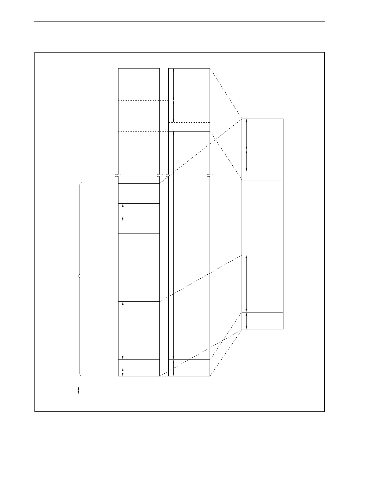
CHAPTER 3 CPU FUNCTION
Figure 3-12. Recommended Memory Map
FFFFFFFFH
FFFFF000H
FFFFEFFFH
FFFF0000H
FFFEFFFFH
04000000H
03FFFFFFH
03FFF000H
03FFEFFFH
03FFA000H
03FF9FFFH
03FF0000H
03FEFFFFH
Use prohibited
Internal RAM
Data spaceProgram space
On-chip
peripheral I/O
Internal RAM
On-chip
peripheral I/O
Internal RAM
Use prohibited
FFFFFFFFH
FFFFF000H
FFFFEFFFH
FFFFA000H
FFFF9FFFH
FFFF0000H
FFFEFFFFH
Program space
64 MB
01000000H
00FFFFFFH
00100000H
000FFFFFH
00080000H
0007FFFFH
00000000H
Use prohibited
External
memory
Internal ROM
Internal ROM
Remarks 1.
indicates the recommended area.
2. This figure is the recommended memory map of the μPD70F3712.
External
memory
00100000H
000FFFFFH
Internal ROM
00000000H
70
User’s Manual U17717EJ3V0UD

CHAPTER 3 CPU FUNCTION
3.4.6 Peripheral I/O registers
Address Function Register Name Symbol R/W
FFFFF004H Port DL PDL √ Undefined
FFFFF004H Port DLL PDLL
FFFFF005H Port DLH PDLH
FFFFF008H Port CS PCS
FFFFF00AH Port CT PCT
FFFFF00CH Port CM PCM
FFFFF00EH Port CD PCD
FFFFF024H Port mode register DL PMDL
FFFFF024H Port mode register DLL PMDLL
FFFFF025H Port mode register DLH PMDLH
FFFFF028H Port mode register CS PMCS
FFFFF02AH Port mode register CT PMCT
FFFFF02CH Port mode register CM PMCM
FFFFF02EH Port mode register CD PMCD
FFFFF044H Port mode control register DL PMCDL
FFFFF044H Port mode control register DLL PMCDLL
FFFFF045H Port mode control register DLH PMCDLH
FFFFF048H Port mode control register CS PMCCS
FFFFF04AH Port mode control register CT PMCCT
FFFFF04CH Port mode control register CM PMCCM
FFFFF066H Bus size configuration register BSC
FFFFF06EH System wait control register
FFFFF080H DMA source address register 0L DSA0L
FFFFF082H DMA source address register 0H DSA0H
FFFFF084H DMA destination address register 0L DDA0L
FFFFF086H DMA destination address register 0H DDA0H
FFFFF088H DMA source address register 1L DSA1L
FFFFF08AH DMA source address register 1H DSA1H
FFFFF08CH DMA destination address register 1L DDA1L
FFFFF08EH DMA destination address register 1H DDA1H
FFFFF090H DMA source address register 2L DSA2L
FFFFF092H DMA source address register 2H DSA2H
FFFFF094H DMA destination address register 2L DDA2L
FFFFF096H DMA destination address register 2H DDA2H
FFFFF098H DMA source address register 3L DSA3L
FFFFF09AH DMA source address register 3H DSA3H
FFFFF09CH DMA destination address register 3L DDA3L
FFFFF09EH DMA destination address register 3H DDA3H
FFFFF0C0H DMA transfer count register 0 DBC0
FFFFF0C2H DMA transfer count register 1 DBC1
FFFFF0C4H DMA transfer count register 2 DBC2
FFFFF0C6H DMA transfer count register 3 DBC3
VSWC
Manipulatable Bits
1 8 16
R/W
√ √
√ √
√ √
√ √
√ √
√ √
√ √
√ √
√ √
√ √
√ √
√ √
√ √
√ √
√ √
√ √
√ √
Default Value
Undefined
Undefined
Undefined
Undefined
Undefined
Undefined
FFFFH
√
FFH
FFH
FFH
FFH
FFH
FFH
0000H
√
00H
00H
00H
00H
00H
5555H
√
77H
√
Undefined
√
Undefined
√
Undefined
√
Undefined
√
Undefined
√
Undefined
√
Undefined
√
Undefined
√
Undefined
√
Undefined
√
Undefined
√
Undefined
√
Undefined
√
Undefined
√
Undefined
√
Undefined
√
Undefined
√
Undefined
√
Undefined
√
√ Undefined
(1/11)
User’s Manual U17717EJ3V0UD
71

CHAPTER 3 CPU FUNCTION
Address Function Register Name Symbol R/W
FFFFF0D0H DMA addressing control register 0 DADC0
FFFFF0D2H DMA addressing control register 1 DADC1
FFFFF0D4H DMA addressing control register 2 DADC2
FFFFF0D6H DMA addressing control register 3 DADC3
FFFFF0E0H DMA channel control register 0 DCHC0
FFFFF0E2H DMA channel control register 1 DCHC1
FFFFF0E4H DMA channel control register 2 DCHC2
FFFFF0E6H DMA channel control register 3 DCHC3
FFFFF100H Interrupt mask register 0 IMR0
FFFFF100H Interrupt mask register 0L IMR0L
FFFFF101H Interrupt mask register 0H IMR0H
FFFFF102H Interrupt mask register 1 IMR1
FFFFF102H Interrupt mask register 1L IMR1L
FFFFF103H Interrupt mask register 1H IMR1H
FFFFF104H Interrupt mask register 2 IMR2
FFFFF104H Interrupt mask register 2L IMR2L
FFFFF105H Interrupt mask register 2H IMR2H
FFFFF106H Interrupt mask register 3 IMR3
FFFFF106H Interrupt mask register 3L IMR3L
FFFFF107H Interrupt mask register 3H IMR3H
FFFFF108H Interrupt mask register 4 IMR4
FFFFF108H Interrupt mask register 4L IMR4L
FFFFF109H Interrupt mask register 4H IMR4H
FFFFF110H Interrupt control register LVIIC
FFFFF112H Interrupt control register PIC0
FFFFF114H Interrupt control register PIC1
FFFFF116H Interrupt control register PIC2
FFFFF118H Interrupt control register PIC3
FFFFF11AH Interrupt control register PIC4
FFFFF11CH Interrupt control register PIC5
FFFFF11EH Interrupt control register PIC6
FFFFF120H Interrupt control register PIC7
FFFFF122H Interrupt control register TQ0OVIC
FFFFF124H Interrupt control register TQ0CCIC0
FFFFF126H Interrupt control register TQ0CCIC1
FFFFF128H Interrupt control register TQ0CCIC2
FFFFF12AH Interrupt control register TQ0CCIC3
FFFFF12CH Interrupt control register TP0OVIC
FFFFF12EH Interrupt control register TP0CCIC0
FFFFF130H Interrupt control register TP0CCIC1
FFFFF132H Interrupt control register TP1OVIC
FFFFF134H Interrupt control register TP1CCIC0
Manipulatable Bits
1 8 16
R/W
√ √
√ √
√ √
√ √
√ √
√ √
√ √
√ √
√ √
√ √
√ √
√ √
√ √
√ √
√ √
√ √
√ √
√ √
√ √
√ √
√ √
√ √
√ √
√ √
√ √
√ √
√ √
√ √
√ √
√ √
√ √
√ √
√ √
Default Value
0000H
√
0000H
√
0000H
√
0000H
√
00H
00H
00H
00H
FFFFH
√
FFH
FFH
FFFFH
√
FFH
FFH
FFFFH
√
FFH
FFH
FFFFH
√
FFH
FFH
FFFFH
√
FFH
FFH
47H
47H
47H
47H
47H
47H
47H
47H
47H
47H
47H
47H
47H
47H
47H
47H
47H
47H
47H
(2/11)
72
User’s Manual U17717EJ3V0UD

CHAPTER 3 CPU FUNCTION
Address Function Register Name Symbol R/W
FFFFF136H Interrupt control register TP1CCIC1
FFFFF138H Interrupt control register TP2OVIC
FFFFF13AH Interrupt control register TP2CCIC0
FFFFF13CH Interrupt control register TP2CCIC1
FFFFF13EH Interrupt control register TP3OVIC
FFFFF140H Interrupt control register TP3CCIC0
FFFFF142H Interrupt control register TP3CCIC1
FFFFF144H Interrupt control register TM0EQIC0
FFFFF146H Interrupt control register CB0RIC
FFFFF148H Interrupt control register CB0TIC
FFFFF14AH Interrupt control register CB1RIC
FFFFF14CH Interrupt control register CB1TIC
FFFFF14EH Interrupt control register UA0RIC
FFFFF150H Interrupt control register UA0TIC
FFFFF152H Interrupt control register UA1RIC
FFFFF154H Interrupt control register UA1TIC
FFFFF156H Interrupt control register ADIC
FFFFF160H Interrupt control register KRIC
FFFFF162H Interrupt control register
FFFFF164H Interrupt control register WTIC
FFFFF166H Interrupt control register PIC8
FFFFF168H Interrupt control register PIC9
FFFFF16AH Interrupt control register PIC10
FFFFF16CH Interrupt control register TQ1OVIC
FFFFF16EH Interrupt control register TQ1CCIC0
FFFFF170H Interrupt control register TQ1CCIC1
FFFFF172H Interrupt control register TQ1CCIC2
FFFFF174H Interrupt control register TQ1CCIC3
FFFFF176H Interrupt control register UA2RIC
FFFFF178H Interrupt control register UA2TIC
FFFFF182H Interrupt control register DMAIC0
FFFFF184H Interrupt control register DMAIC1
FFFFF186H Interrupt control register DMAIC2
FFFFF188H Interrupt control register DMAIC3
FFFFF18AH Interrupt control register PIC11
FFFFF18CH Interrupt control register PIC12
FFFFF18EH Interrupt control register PIC13
FFFFF190H Interrupt control register PIC14
FFFFF192H Interrupt control register TQ2OVIC
FFFFF194H Interrupt control register TQ2CCIC0
FFFFF196H Interrupt control register TQ2CCIC1
FFFFF198H Interrupt control register TQ2CCIC2
WTIIC
Manipulatable Bits
1 8 16
R/W
√ √
√ √
√ √
√ √
√ √
√ √
√ √
√ √
√ √
√ √
√ √
√ √
√ √
√ √
√ √
√ √
√ √
√ √
√ √
√ √
√ √
√ √
√ √
√ √
√ √
√ √
√ √
√ √
√ √
√ √
√ √
√ √
√ √
√ √
√ √
√ √
√ √
√ √
√ √
√ √
√ √
√ √
(3/11)
Default Value
47H
47H
47H
47H
47H
47H
47H
47H
47H
47H
47H
47H
47H
47H
47H
47H
47H
47H
47H
47H
47H
47H
47H
47H
47H
47H
47H
47H
47H
47H
47H
47H
47H
47H
47H
47H
47H
47H
47H
47H
47H
47H
User’s Manual U17717EJ3V0UD
73

CHAPTER 3 CPU FUNCTION
Address Function Register Name Symbol R/W
FFFFF19AH Interrupt control register TQ2CCIC3
FFFFF19CH Interrupt control register CB2RIC
FFFFF19EH Interrupt control register CB2TIC
FFFFF1A0H Interrupt control register UA3RIC
FFFFF1A2H Interrupt control register UA3TIC
Note
Note
FFFFF1FAH In-service priority register ISPR R
Manipulatable Bits
1 8 16
R/W
√ √
√ √
√ √
√ √
√ √
√ √
FFFFF1FCH Command register PRCMD W
FFFFF1FEH Power save control register PSC
FFFFF200H A/D converter mode register 0 ADA0M0
FFFFF201H A/D converter mode register 1 ADA0M1
FFFFF202H A/D converter channel specification register ADA0S
FFFFF203H A/D converter mode register 2 ADA0M2
FFFFF204H Power-fail compare mode register ADA0PFM
FFFFF205H Power-fail compare threshold value register ADA0PFT
FFFFF210H A/D conversion result register 0 ADA0CR0
R/W
R
√ √
√ √
√ √
√ √
√ √
√ √
√ √
FFFFF211H A/D conversion result register 0H ADA0CR0H
FFFFF212H A/D conversion result register 1 ADA0CR1
FFFFF213H A/D conversion result register 1H ADA0CR1H
FFFFF214H A/D conversion result register 2 ADA0CR2
FFFFF215H A/D conversion result register 2H ADA0CR2H
FFFFF216H A/D conversion result register 3 ADA0CR3
FFFFF217H A/D conversion result register 3H ADA0CR3H
FFFFF218H A/D conversion result register 4 ADA0CR4
FFFFF219H A/D conversion result register 4H ADA0CR4H
FFFFF21AH A/D conversion result register 5 ADA0CR5
FFFFF21BH A/D conversion result register 5H ADA0CR5H
FFFFF21CH A/D conversion result register 6 ADA0CR6
FFFFF21DH A/D conversion result register 6H ADA0CR6H
FFFFF21EH A/D conversion result register 7 ADA0CR7
FFFFF21FH A/D conversion result register 7H ADA0CR7H
FFFFF220H A/D conversion result register 8 ADA0CR8
FFFFF221H A/D conversion result register 8H ADA0CR8H
FFFFF222H A/D conversion result register 9 ADA0CR9
FFFFF223H A/D conversion result register 9H ADA0CR9H
FFFFF224H A/D conversion result register 10 ADA0CR10
FFFFF225H A/D conversion result register 10H ADA0CR10H
FFFFF226H A/D conversion result register 11 ADA0CR11
FFFFF227H A/D conversion result register 11H ADA0CR11H
FFFFF228H A/D conversion result register 12 ADA0CR12
FFFFF229H A/D conversion result register 12H ADA0CR12H
Note
μ
PD70F3711, 70F3712 only
47H
47H
47H
47H
47H
00H
Undefined
√
00H
00H
00H
00H
00H
00H
00H
√
Undefined
√
√
Undefined
√
√
Undefined
√
√
Undefined
√
√
Undefined
√
√
Undefined
√
√
Undefined
√
√
Undefined
√
√
Undefined
√
√
Undefined
√
√
Undefined
√
√
Undefined
√
√
Undefined
√
(4/11)
Default Value
Undefined
Undefined
Undefined
Undefined
Undefined
Undefined
Undefined
Undefined
Undefined
Undefined
Undefined
Undefined
Undefined
74
User’s Manual U17717EJ3V0UD
CHAPTER 3 CPU FUNCTION
Address Function Register Name Symbol R/W
FFFFF22AH A/D conversion result register 13 ADA0CR13
FFFFF22BH A/D conversion result register 13H ADA0CR13H
FFFFF22CH A/D conversion result register 14 ADA0CR14
FFFFF22DH A/D conversion result register 14H ADA0CR14H
FFFFF22EH A/D conversion result register 15 ADA0CR15
FFFFF22FH A/D conversion result register 15H ADA0CR15H
FFFFF230H A/D conversion result register 16 ADA0CR16
FFFFF231H A/D conversion result register 16H ADA0CR16H
FFFFF232H A/D conversion result register 17 ADA0CR17
FFFFF233H A/D conversion result register 17H ADA0CR17H
FFFFF234H A/D conversion result register 18 ADA0CR18
FFFFF235H A/D conversion result register 18H ADA0CR18H
FFFFF236H A/D conversion result register 19 ADA0CR19
FFFFF237H A/D conversion result register 19H ADA0CR19H
FFFFF238H A/D conversion result register 20 ADA0CR20
FFFFF239H A/D conversion result register 20H ADA0CR20H
FFFFF23AH A/D conversion result register 21 ADA0CR21
FFFFF23BH A/D conversion result register 21H ADA0CR21H
FFFFF23CH A/D conversion result register 22 ADA0CR22
FFFFF23DH A/D conversion result register 22H ADA0CR22H
FFFFF23EH A/D conversion result register 23 ADA0CR23
FFFFF23FH A/D conversion result register 23H ADA0CR23H
FFFFF300H Key return mode register KRM
FFFFF308H Selector operation control register 0 SELCNT0
FFFFF318H Noise elimination control register NFC
FFFFF400H Port 0 P0
FFFFF402H Port 1 P1
FFFFF406H Port 3 P3 √ Undefined
FFFFF406H Port 3L P3L
FFFFF407H Port 3H P3H
FFFFF408H Port 4 P4
FFFFF40AH Port 5 P5
FFFFF40CH Port 6 P6 √ Undefined
FFFFF40CH Port 6L P6L
FFFFF40DH Port 6H P6H
FFFFF40EH Port 7L P7L
FFFFF40FH Port 7H P7H
FFFFF410H Port 8 P8
FFFFF412H Port 9 P9 √ Undefined
FFFFF412H Port 9L P9L
FFFFF413H Port 9H P9H
FFFFF418H Port 12 P12
Manipulatable Bits
1 8 16
R
R/W
√ √
√ √
√ √
√ √
√ √
√ √
√ √
√ √
√ √
√ √
√ √
√ √
√ √
√ √
√ √
√ √
√ √
Default Value
Undefined
√
Undefined
√
Undefined
√
Undefined
√
Undefined
√
Undefined
√
Undefined
√
Undefined
√
Undefined
√
Undefined
√
Undefined
√
Undefined
√
Undefined
√
Undefined
√
Undefined
√
Undefined
√
Undefined
√
Undefined
√
Undefined
√
Undefined
√
Undefined
√
Undefined
√
00H
00H
00H
Undefined
Undefined
Undefined
Undefined
Undefined
Undefined
Undefined
Undefined
Undefined
Undefined
Undefined
Undefined
Undefined
Undefined
(5/11)
User’s Manual U17717EJ3V0UD
75

CHAPTER 3 CPU FUNCTION
Address Function Register Name Symbol R/W
FFFFF420H Port mode register 0 PM0
FFFFF422H Port mode register 1 PM1
FFFFF426H Port mode register 3 PM3
FFFFF426H Port mode register 3L PM3L
FFFFF427H Port mode register 3H PM3H
FFFFF428H Port mode register 4 PM4
FFFFF42AH Port mode register 5 PM5
FFFFF42CH Port mode register 6 PM6
FFFFF42CH Port mode register 6L PM6L
FFFFF42DH Port mode register 6H PM6H
FFFFF42EH Port mode register 7L PM7L
FFFFF42FH Port mode register 7H PM7H
FFFFF430H Port mode register 8 PM8
FFFFF432H Port mode register 9 PM9
FFFFF432H Port mode register 9L PM9L
FFFFF433H Port mode register 9H PM9H
FFFFF438H Port mode register 12 PM12
FFFFF440H Port mode control register 0 PMC0
FFFFF442H Port mode control register 1 PMC1
FFFFF446H Port mode control register 3 PMC3
FFFFF446H Port mode control register 3L PMC3L
FFFFF447H Port mode control register 3H PMC3H
FFFFF448H Port mode control register 4 PMC4
FFFFF44AH Port mode control register 5 PMC5
FFFFF44CH Port mode control register 6 PMC6
FFFFF44CH Port mode control register 6L PMC6L
FFFFF44DH Port mode control register 6H PMC6H
FFFFF450H Port mode control register 8 PMC8
FFFFF452H Port mode control register 9 PMC9
FFFFF452H Port mode control register 9L PMC9L
FFFFF453H Port mode control register 9H PMC9H
FFFFF460H Port function control register 0 PFC0
FFFFF466H Port function control register 3L PFC3L
FFFFF46AH Port function control register 5 PFC5
FFFFF46CH Port function control register 6 PFC6
FFFFF46CH Port function control register 6L PFC6L
FFFFF46DH Port function control register 6H PFC6H
FFFFF472H Port function control register 9 PFC9
FFFFF472H Port function control register 9L PFC9L
FFFFF473H Port function control register 9H PFC9H
FFFFF484H Data wait control register 0 DWC0
FFFFF488H Address wait control register AWC
Manipulatable Bits
1 8 16
R/W
√ √
√ √
√ √
√ √
√ √
√ √
√ √
√ √
√ √
√ √
√ √
√ √
√ √
√ √
√ √
√ √
√ √
√ √
√ √
√ √
√ √
√ √
√ √
√ √
√ √
√ √
√ √
√ √
√ √
√ √
√ √
√ √
√ FFFFH
Default Value
FFH
FFH
FFFFH
√
FFH
FFH
FFH
FFH
FFFFH
√
FFH
FFH
FFH
FFH
FFH
FFFFH
√
FFH
FFH
FFH
00H
00H
0000H
√
00H
00H
00H
00H
0000H
√
00H
00H
00H
0000H
√
00H
00H
00H
00H
00H
0000H
√
00H
00H
0000H
√
00H
00H
7777H
√
(6/11)
76
User’s Manual U17717EJ3V0UD

CHAPTER 3 CPU FUNCTION
Address Function Register Name Symbol R/W
FFFFF48AH Bus cycle control register BCC
FFFFF540H TMQ0 control register 0 TQ0CTL0
FFFFF541H TMQ0 control register 1 TQ0CTL1
FFFFF542H TMQ0 I/O control register 0 TQ0IOC0
FFFFF543H TMQ0 I/O control register 1 TQ0IOC1
FFFFF544H TMQ0 I/O control register 2 TQ0IOC2
FFFFF545H TMQ0 option register 0 TQ0OPT0
FFFFF546H TMQ0 capture/compare register 0 TQ0CCR0
FFFFF548H TMQ0 capture/compare register 1 TQ0CCR1
FFFFF54AH TMQ0 capture/compare register 2 TQ0CCR2
FFFFF54CH TMQ0 capture/compare register 3 TQ0CCR3
FFFFF54EH TMQ0 counter read buffer register TQ0CNT R
FFFFF590H TMP0 control register 0 TP0CTL0
FFFFF591H TMP0 control register 1 TP0CTL1
FFFFF592H TMP0 I/O control register 0 TP0IOC0
FFFFF593H TMP0 I/O control register 1 TP0IOC1
FFFFF594H TMP0 I/O control register 2 TP0IOC2
FFFFF595H TMP0 option register 0 TP0OPT0
FFFFF596H TMP0 capture/compare register 0 TP0CCR0
FFFFF598H TMP0 capture/compare register 1 TP0CCR1
FFFFF59AH TMP0 counter read buffer register TP0CNT R
FFFFF5A0H TMP1 control register 0 TP1CTL0
FFFFF5A1H TMP1 control register 1 TP1CTL1
FFFFF5A2H TMP1 I/O control register 0 TP1IOC0
FFFFF5A3H TMP1 I/O control register 1 TP1IOC1
FFFFF5A4H TMP1 I/O control register 2 TP1IOC2
FFFFF5A5H TMP1 option register 0 TP1OPT0
FFFFF5A6H TMP1 capture/compare register 0 TP1CCR0
FFFFF5A8H TMP1 capture/compare register 1 TP1CCR1
FFFFF5AAH TMP1 counter read buffer register TP1CNT R
FFFFF5B0H TMP2 control register 0 TP2CTL0
FFFFF5B1H TMP2 control register 1 TP2CTL1
FFFFF5B2H TMP2 I/O control register 0 TP2IOC0
FFFFF5B3H TMP2 I/O control register 1 TP2IOC1
FFFFF5B4H TMP2 I/O control register 2 TP2IOC2
FFFFF5B5H TMP2 option register 0 TP2OPT0
FFFFF5B6H TMP2 capture/compare register 0 TP2CCR0
FFFFF5B8H TMP2 capture/compare register 1 TP2CCR1
FFFFF5BAH TMP2 counter read buffer register TP2CNT R
FFFFF5C0H TMP3 control register 0 TP3CTL0
FFFFF5C1H TMP3 control register 1 TP3CTL1
FFFFF5C2H TMP3 I/O control register 0 TP3IOC0
Manipulatable Bits
1 8 16
R/W
√ √
√ √
√ √
√ √
√ √
√ √
R/W
R/W
R/W
R/W
√ √
√ √
√ √
√ √
√ √
√ √
√ √
√ √
√ √
√ √
√ √
√ √
√ √
√ √
√ √
√ √
√ √
√ √
√ √
√ √
√ √
√ 0000H
√ 0000H
√ 0000H
√ 0000H
Default Value
AAAAH
√
00H
00H
00H
00H
00H
00H
0000H
√
0000H
√
0000H
√
0000H
√
00H
00H
00H
00H
00H
00H
0000H
√
0000H
√
00H
00H
00H
00H
00H
00H
0000H
√
0000H
√
00H
00H
00H
00H
00H
00H
0000H
√
0000H
√
00H
00H
00H
(7/11)
User’s Manual U17717EJ3V0UD
77

CHAPTER 3 CPU FUNCTION
Address Function Register Name Symbol R/W
FFFFF5C3H TMP3 I/O control register 1 TP3IOC1
FFFFF5C4H TMP3 I/O control register 2 TP3IOC2
FFFFF5C5H TMP3 option register 0 TP3OPT0
FFFFF5C6H TMP3 capture/compare register 0 TP3CCR0
FFFFF5C8H TMP3 capture/compare register 1 TP3CCR1
FFFFF5CAH TMP3 counter read buffer register TP3CNT R
FFFFF610H TMQ1 control register 0 TQ1CTL0
FFFFF611H TMQ1 control register 1 TQ1CTL1
FFFFF612H TMQ1 I/O control register 0 TQ1IOC0
FFFFF613H TMQ1 I/O control register 1 TQ1IOC1
FFFFF614H TMQ1 I/O control register 2 TQ1IOC2
FFFFF615H TMQ1 timer option register 0 TQ1OPT0
FFFFF616H TMQ1 capture/compare register 0 TQ1CCR0
FFFFF618H TMQ1 capture/compare register 1 TQ1CCR1
FFFFF61AH TMQ1 capture/compare register 2 TQ1CCR2
FFFFF61CH TMQ1 capture/compare register 3 TQ1CCR3
FFFFF61EH TMQ1 counter read buffer register TQ1CNT R
FFFFF620H TMQ2 control register 0 TQ2CTL0
FFFFF621H TMQ2 control register 1 TQ2CTL1
FFFFF622H TMQ2 I/O control register 0 TQ2IOC0
FFFFF623H TMQ2 I/O control register 1 TQ2IOC1
FFFFF624H TMQ2 I/O control register 2 TQ2IOC2
FFFFF625H TMQ2 timer option register 0 TQ2OPT0
FFFFF626H TMQ2 capture/compare register 0 TQ2CCR0
FFFFF628H TMQ2 capture/compare register 1 TQ2CCR1
FFFFF62AH TMQ2 capture/compare register 2 TQ2CCR2
FFFFF62CH TMQ2 capture/compare register 3 TQ2CCR3
FFFFF62EH TMQ2 counter read buffer register TQ2CNT R
FFFFF680H Watch timer operation mode register WTM
FFFFF690H TMM0 control register 0 TM0CTL0
FFFFF694H TMM0 compare register 0 TM0CMP0
FFFFF6C0H Oscillation stabilization time select register OSTS
FFFFF6C1H PLL lockup time specification register PLLS
FFFFF6D0H Watchdog timer mode register 2 WDTM2
FFFFF6D1H Watchdog timer enable register WDTE
FFFFF706H Port function control expansion register 3L PFCE3L
FFFFF70AH Port function control expansion register 5 PFCE5
FFFFF712H Port function control expansion register 9 PFCE9
FFFFF712H Port function control expansion register 9L PFCE9L
FFFFF713H Port function control expansion register 9H PFCE9H
FFFFF802H System status register SYS
FFFFF80CH Internal oscillation mode register RCM
Manipulatable Bits
1 8 16
R/W
R/W
R/W
R/W
√ √
√ √
√ √
√ 0000H
√ √
√ √
√ √
√ √
√ √
√ √
√ 0000H
√ √
√ √
√ √
√ √
√ √
√ 0000H
√ √
√ √
√ √
√ √
√ √
√ √
√ √
√ √
√ √
√
√
√
Default Value
00H
00H
00H
0000H
√
0000H
√
00H
00H
00H
00H
00H
00H
0000H
√
0000H
√
0000H
√
0000H
√
00H
00H
00H
00H
00H
00H
√
0000H
√
0000H
√
0000H
√
0000H
√
00H
00H
0000H
√
06H
03H
67H
9AH
00H
00H
0000H
√
00H
00H
00H
00H
(8/11)
78
User’s Manual U17717EJ3V0UD

CHAPTER 3 CPU FUNCTION
Address Function Register Name Symbol R/W
FFFFF810H DMA trigger factor register 0 DTFR0
FFFFF812H DMA trigger factor register 1 DTFR1
FFFFF814H DMA trigger factor register 2 DTFR2
FFFFF816H DMA trigger factor register 3 DTFR3
FFFFF820H Power save mode register PSMR
FFFFF824H Lock register LOCKR R
FFFFF828H Processor clock control register PCC
FFFFF82CH PLL control register PLLCTL
FFFFF82EH CPU operating clock status register CCLS R
FFFFF82FH Programmable clock mode register PCLM
FFFFF870H Clock monitor mode register CLM
FFFFF888H Reset source flag register RESF
FFFFF890H Low-voltage detection register LVIM
FFFFF891H Low-voltage detection level select register LVIS
FFFFF892H Internal RAM data status register RAMS
FFFFF8B0H Prescaler mode register 0 PRSM0
FFFFF8B1H Prescaler compare register 0 PRSCM0
FFFFF9FCH On-chip debug mode register OCDM
FFFFF9FEH Peripheral emulation register 1 PEMU1
FFFFFA00H UARTA0 control register 0 UA0CTL0
FFFFFA01H UARTA0 control register 1 UA0CTL1
FFFFFA02H UARTA0 control register 2 UA0CTL2
FFFFFA03H UARTA0 option control register 0 UA0OPT0
FFFFFA04H UARTA0 status register UA0STR
FFFFFA06H UARTA0 receive data register UA0RX R
FFFFFA07H UARTA0 transmit data register UA0TX
FFFFFA10H UARTA1 control register 0 UA1CTL0
FFFFFA11H UARTA1 control register 1 UA1CTL1
FFFFFA12H UARTA1 control register 2 UA1CTL2
FFFFFA13H UARTA1 option control register 0 UA1OPT0
FFFFFA14H UARTA1 status register UA1STR
FFFFFA16H UARTA1 receive data register UA1RX R
FFFFFA17H UARTA1 receive data register UA1TX
FFFFFA20H UARTA2 control register 0 UA2CTL0
FFFFFA21H UARTA2 control register 1 UA2CTL1
FFFFFA22H UARTA2 control register 2 UA2CTL2
FFFFFA23H UARTA2 option control register 0 UA2OPT0
FFFFFA24H UARTA2 status register UA2STR
FFFFFA26H UARTA2 receive data register UA2RX R
FFFFFA27H UARTA2 transmit data register UA2TX R/W
Manipulatable Bits
1 8 16
R/W
R/W
R/W
R/W
R/W
√ √
√ √
√ √
√ √
√ √
√ √
√ √
√ √
√ √
√ √
√ √
√ √
√ √
√ √
√ √
√ √
√ √
√ √
√ √
√ √
√ √
√ √
√ √
√ √
√ √
Caution For details of the OCDM register, see CHAPTER 26 ON-CHIP DEBUG FUNCTION.
√
√
√
√
√
√
√
√
√
√
√
√
√
√
√
Default Value
00H
00H
00H
00H
00H
00H
03H
01H
00H
00H
00H
00H
00H
00H
01H
00H
00H
01H
00H
10H
00H
FFH
14H
00H
FFH
FFH
10H
00H
FFH
14H
00H
FFH
FFH
10H
00H
FFH
14H
00H
FFH
FFH
(9/11)
User’s Manual U17717EJ3V0UD
79

CHAPTER 3 CPU FUNCTION
Address Function Register Name Symbol R/W
FFFFFA30H UARTA3 control register 0 UA3CTL0
FFFFFA31H UARTA3 control register 1 UA3CTL1
FFFFFA32H UARTA3 control register 2 UA3CTL2
FFFFFA33H UARTA3 option control register 0 UA3OPT0
FFFFFA34H UARTA3 status register UA3STR
FFFFFA36H UARTA3 receive data register UA3RX
FFFFFA37H UARTA3 transmit data register UA3TX
Note
Note
√ 00H
Note
√ FFH
Note
Note
Note
R √ FFH
Note
√ FFH
FFFFFB00H TIP00 pin noise elimination control register P00NFC
FFFFFB04H TIP01 pin noise elimination control register P01NFC
FFFFFB08H TIP10 pin noise elimination control register P10NFC
FFFFFB0CH TIP11 pin noise elimination control register P11NFC
FFFFFB10H TIP20 pin noise elimination control register P20NFC
FFFFFB14H TIP21 pin noise elimination control register P21NFC
FFFFFB18H TIP30 pin noise elimination control register P30NFC
FFFFFB1CH TIP31 pin noise elimination control register P31NFC
FFFFFB50H TIQ00 pin noise elimination control register Q00NFC
FFFFFB54H TIQ01 pin noise elimination control register Q01NFC
FFFFFB58H TIQ02 pin noise elimination control register Q02NFC
FFFFFB5CH TIQ03 pin noise elimination control register Q03NFC
FFFFFB60H TIQ10 pin noise elimination control register Q10NFC
FFFFFB64H TIQ11 pin noise elimination control register Q11NFC
FFFFFB68H TIQ12 pin noise elimination control register Q12NFC
FFFFFB6CH TIQ13 pin noise elimination control register Q13NFC
FFFFFB70H TIQ20 pin noise elimination control register Q20NFC
FFFFFB74H TIQ21 pin noise elimination control register Q21NFC
FFFFFB78H TIQ22 pin noise elimination control register Q22NFC
FFFFFB7CH TIQ23 pin noise elimination control register Q23NFC
FFFFFC00H External interrupt falling edge specification register 0 INTF0
FFFFFC02H External interrupt falling edge specification register 1 INTF1
Manipulatable Bits
1 8 16
R/W
√ √
√ √
√ √
R/W
√ √
√ √
√ √
√ √
√ √
√ √
√ √
√ √
√ √
√ √
√ √
√ √
√ √
√ √
√ √
√ √
√ √
√ √
√ √
√ √
√ √
√ √
FFFFFC06H External interrupt falling edge specification register 3 INTF3
FFFFFC06H External interrupt falling edge specification register 3L INTF3L
FFFFFC07H External interrupt falling edge specification register 3H INTF3H
FFFFFC0CH External interrupt falling edge specification register 6L INTF6L
FFFFFC10H External interrupt falling edge specification register 8 INTF8
FFFFFC13H External interrupt falling edge specification register 9H INTF9H
FFFFFC20H External interrupt rising edge specification register 0 INTR0
FFFFFC22H External interrupt rising edge specification register 1 INTR1
√ √
√ √
√ √
√ √
√ √
√ √
√ √
Note
μ
PD70F3711, 70F3712 only
Default Value
10H
14H
00H
00H
00H
00H
00H
00H
00H
00H
00H
00H
00H
00H
00H
00H
00H
00H
00H
00H
00H
00H
00H
00H
00H
0000H
√
00H
00H
00H
00H
00H
00H
00H
(10/11)
80
User’s Manual U17717EJ3V0UD

CHAPTER 3 CPU FUNCTION
Address Function Register Name Symbol R/W
FFFFFC26H External interrupt rising edge specification register 3 INTR3
FFFFFC26H External interrupt rising edge specification register 3L INTR3L
FFFFFC27H External interrupt rising edge specification register 3H INTR3H
FFFFFC2CH External interrupt rising edge specification register 6L INTR6L
FFFFFC30H External interrupt rising edge specification register 8 INTR8
FFFFFC33H External interrupt rising edge specification register 9H INTR9H
FFFFFC40H Pull-up resistor option register 0 PU0
FFFFFC42H Pull-up resistor option register 1 PU1
FFFFFC46H Pull-up resistor option register 3 PU3
FFFFFC46H Pull-up resistor option register 3L PU3L
FFFFFC47H Pull-up resistor option register 3H PU3H
FFFFFC48H Pull-up resistor option register 4 PU4
FFFFFC4AH Pull-up resistor option register 5 PU5
FFFFFC4CH Pull-up resistor option register 6 PU6
FFFFFC4CH Pull-up resistor option register 6L PU6L
FFFFFC4DH Pull-up resistor option register 6H PU6H
FFFFFC50H Pull-up resistor option register 8 PU8
FFFFFC52H Pull-up resistor option register 9 PU9
FFFFFC52H Pull-up resistor option register 9L PU9L
FFFFFC53H Pull-up resistor option register 9H PU9H
FFFFFD00H CSIB0 control register 0 CB0CTL0
FFFFFD01H CSIB0 control register 1 CB0CTL1
FFFFFD02H CSIB0 control register 2 CB0CTL2
FFFFFD03H CSIB0 status register CB0STR
FFFFFD04H CSIB0 receive data register CB0RX
FFFFFD04H CSIB0 receive data register L CB0RXL
FFFFFD06H CSIB0 transmit data register CB0TX
FFFFFD06H CSIB0 transmit data register L CB0TXL
FFFFFD10H CSIB1 control register 0 CB1CTL0
FFFFFD11H CSIB1 control register 1 CB1CTL1
FFFFFD12H CSIB1 control register 2 CB1CTL2
FFFFFD13H CSIB1 status register CB1STR
FFFFFD14H CSIB1 receive data register CB1RX
FFFFFD14H CSIB1 receive data register L CB1RXL
FFFFFD16H CSIB1 transmit data register CB1TX
FFFFFD16H CSIB1 transmit data register L CB1TXL
FFFFFD20H CSIB2 control register 0 CB2CTL0
FFFFFD21H CSIB2 control register 1 CB2CTL1
FFFFFD22H CSIB2 control register 2 CB2CTL2
FFFFFD23H CSIB2 status register CB2STR
FFFFFD24H CSIB2 receive data register CB2RX
FFFFFD24H CSIB2 receive data register L CB2RXL
FFFFFD26H CSIB2 transmit data register CB2TX
FFFFFD26H CSIB2 transmit data register L CB2TXL
Manipulatable Bits
R/W
R
R/W
R
R/W
R
R/W
1 8 16
√ √
√ √
√ √
√ √
√ √
√ √
√ √
√ √
√ √
√ √
√ √
√ √
√ √
√ √
√ √
√ √
√ √
√ √
√
√ √
√
√
√ √
√ √
√
√ √
√
√
√ √
√ √
√
√ √
√
√
Default Value
0000H
√
00H
00H
00H
00H
00H
00H
00H
0000H
√
00H
00H
00H
00H
0000H
√
00H
00H
00H
0000H
√
00H
00H
01H
00H
00H
00H
0000H
√
00H
0000H
√
00H
01H
00H
00H
00H
0000H
√
00H
0000H
√
00H
01H
00H
00H
00H
0000H
√
00H
0000H
√
00H
(11/11)
User’s Manual U17717EJ3V0UD
81

CHAPTER 3 CPU FUNCTION
3.4.7 Special registers
Special registers are registers that are protected from being written with illegal data due to a program hang-up. The
V850ES/HJ2 has the following seven special registers.
• Power save control register (PSC)
• Processor clock control register (PCC)
• Clock monitor mode register (CLM)
• Reset source flag register (RESF)
• Low-voltage detection register (LVIM)
• Internal RAM data status register (RAMS)
• On-chip debug mode register (OCDM)
In addition, the PRCDM register is provided to protect against a write access to the special registers so that the
application system does not inadvertently stop due to a program hang-up. A write access to the special registers is
<R>
made in a specific sequence, and an illegal store operation is reported to the SYS register (reported even when the
read operation of the option data (address: 007AH) is illegal because of noise, instantaneous voltage drop, etc.).
82
User’s Manual U17717EJ3V0UD

CHAPTER 3 CPU FUNCTION
(1) Setting data to special registers
Set data to the special registers in the following sequence.
<1> Disable DMA operation.
<2> Prepare data to be set to the special register in a general-purpose register.
<3> Write the data prepared in <2> to the PRCMD register.
<4> Write the setting data to the special register (by using the following instructions).
• Store instruction (ST/SST instruction)
• Bit manipulation instruction (SET1/CLR1/NOT1 instruction)
(<5> to <9> Insert NOP instructions (5 instructions).)
Note
<10> Enable DMA operation if necessary.
[Example] With PSC register (setting standby mode)
ST.B r11, PSMR[r0] ; Set PSMR register (setting IDLE1, IDLE2, and STOP modes).
<1>CLR1 0, DCHCn[r0] ; Disable DMA operation. n = 0 to 3
<2>MOV0x02, r10
<3>ST.B r10, PRCMD[r0] ; Write PRCMD register.
<4>ST.B r10, PSC[r0] ; Set PSC register.
<5>NOP
<6>NOP
<7>NOP
<8>NOP
<9>NOP
Note
; Dummy instruction
Note
; Dummy instruction
Note
; Dummy instruction
Note
; Dummy instruction
Note
; Dummy instruction
<10>SET1 0, DCHCn[r0] ; Enable DMA operation. n = 0 to 3
(next instruction)
There is no special sequence to read a special register.
Note Five NOP instructions or more must be inserted immediately after setting the IDLE1 mode, IDLE2
mode, STOP mode, or sub-IDLE mode (by setting the PSC.STP bit to 1).
Cautions 1. When a store instruction is executed to store data in the command register, interrupts are
not acknowledged. This is because it is assumed that steps <3> and <4> above are
performed by successive store instructions. If another instruction is placed between <3>
and <4>, and if an interrupt is acknowledged by that instruction, the above sequence may
not be established, causing malfunction.
2. Although dummy data is written to the PRCMD register, use the same general-purpose
register used to set the special register (<4> in Example) to write data to the PRCMD
register (<3> in Example). The same applies when a general-purpose register is used for
addressing.
User’s Manual U17717EJ3V0UD
83

CHAPTER 3 CPU FUNCTION
(2) Command register (PRCMD)
The PRCMD register is an 8-bit register that protects the registers that may seriously affect the application
system from being written, so that the system does not inadvertently stop due to a program hang-up. The first
write access to a special register is valid after data has been written in advance to the PRCMD register. In this
way, the value of the special register can be rewritten only in a specific sequence, so as to protect the register
from an illegal write access.
The PRCMD register is write-only, in 8-bit units (undefined data is read when this register is read).
After reset: Undefined W Address: FFFFF1FCH
7
REG7PRCMD
6
REG65REG54REG43REG32REG21REG10REG0
84
User’s Manual U17717EJ3V0UD

CHAPTER 3 CPU FUNCTION
(3) System status register (SYS)
Status flags that indicate the operation status of the overall system are allocated to this register.
This register can be read or written in 8-bit or 1-bit units.
Reset sets this register to 00H.
After reset: 00H R/W Address: FFFFF802H
SYS 0 0 0 0 0 0 PRERR
0
PRERR
0
Protection error did not occur
1
Protection error occurred
The PRERR flag operates under the following conditions.
(a) Set condition (PRERR flag = 1)
(i) When data is written to a special register without writing anything to the PRCMD register (when <4> is
executed without executing <3> in 3.4.7 (1) Setting data to special registers)
(ii) When data is written to an on-chip peripheral I/O register other than a special register (including
execution of a bit manipulation instruction) after writing data to the PRCMD register (if <4> in 3.4.7 (1)
Setting data to special registers is not the setting of a special register)
Remark Between an operation to write the PRCMD register and an operation to write a special register,
even if the internal RAM is accessed, such as reading when an on-chip peripheral I/O register
(except reading by a bit manipulation instruction), the PRERR flag is not set, and the set data
can be written to the special register.
(b) Clear condition (PRERR flag = 0)
(i) When 0 is written to the PRERR flag
(ii) When the system is reset
Cautions 1. If 0 is written to the PRERR bit of the SYS register, which is not a special register,
immediately after a write access to the PRCMD register, the PRERR bit is cleared to 0
(the write access takes precedence).
2. If data is written to the PRCMD register, which is not a special register, immediately
after a write access to the PRCMD register, the PRERR bit is set to 1.
Detects protection error
User’s Manual U17717EJ3V0UD
85

CHAPTER 3 CPU FUNCTION
3.4.8 Cautions
(1) Registers to be set first
Be sure to set the following registers first when using the V850ES/HJ2.
• System wait control register (VSWC)
• On-chip debug mode register (OCDM)
• Watchdog timer mode register 2 (WDTM2)
After setting the VSWC, OCDM, and WDTM2 registers, set the other registers as necessary.
When using the external bus, set each pin to the alternate-function bus control pin mode by using the port-
related registers after setting the above registers.
(a) System wait control register (VSWC)
The VSWC register controls wait of bus access to the on-chip peripheral I/O registers.
Three clocks are required to access an on-chip peripheral I/O register (without a wait cycle). The
V850ES/HJ2 requires wait cycles according to the operating frequency. Set the following value to the
VSWC register in accordance with the frequency used.
The VSWC register can be read or written in 8-bit units (address: FFFFF06EH, default value: 77H).
Operating Frequency (fCLK) Set Value of VSWC Number of Waits
32 kHz ≤ fCLK < 16.6 MHz 00H 0 (no waits)
16.6 MHz ≤ fCLK ≤ 20 MHz 01H 1
(b) On-chip debug mode register (OCDM)
For details, see CHAPTER 26 ON-CHIP DEBUG FUNCTION.
(c) Watchdog timer mode register 2 (WDTM2)
The WDTM2 register sets the overflow time and the operation clock of watchdog timer 2.
Watchdog timer 2 automatically starts in the reset mode after reset is released. Write the WDTM2 register
to activate this operation.
For details, see CHAPTER 11 FUNCTIONS OF WATCHDOG TIMER 2.
86
User’s Manual U17717EJ3V0UD

CHAPTER 3 CPU FUNCTION
(2) Accessing specific on-chip peripheral I/O registers
This product has two types of internal system buses.
One is a CPU bus and the other is a peripheral bus that interfaces with low-speed peripheral hardware.
The clock of the CPU bus and the clock of the peripheral bus are asynchronous. If an access to the CPU and
an access to the peripheral hardware conflict, therefore, unexpected illegal data may be transferred. If there is
a possibility of a conflict, the number of cycles for accessing the CPU changes when the peripheral hardware is
accessed, so that correct data is transferred. As a result, the CPU does not start processing of the next
instruction but enters the wait state. If this wait state occurs, the number of clocks required to execute an
instruction increases by the number of wait clocks shown below.
This must be taken into consideration if real-time processing is required.
When specific on-chip peripheral I/O registers are accessed, more wait states may be required in addition to
the wait states set by the VSWC register.
The access conditions and how to calculate the number of wait states to be inserted (number of CPU clocks)
at this time are shown below.
Peripheral Function Register Name Access k
16-bit timer/event counter P (TMP)
(n = 0 to 3)
16-bit timer/event counter Q (TMQ)
(m = 0 to 2)
Watchdog timer 2 (WDT2) WDTM2 Write
A/D converter
TPnCNT Read 1 or 2
TPnCCR0, TPnCCR1
TQmCNT Read 1 or 2
TQmCCR0 to TQmCCR3
ADA0M0 Read 1 or 2
ADA0CR0 to ADA0CR23 Read 1 or 2
ADA0CR0H to ADA0CR23H Read 1 or 2
Write • 1st access: No wait
• Continuous write: 3 or 4
Read 1 or 2
Write • 1st access: No wait
• Continuous write: 3 or 4
Read 1 or 2
3
(when WDT2 operating)
Number of clocks necessary for access = 3 + i + j + (2 + j) × k
Caution Accessing the above registers is prohibited in the following statuses. If a wait cycle is
generated, it can only be cleared by a reset.
• When the CPU operates with the subclock and the main clock oscillation is stopped
• When the CPU operates with the internal oscillation clock
Remark i: Values (0 or 1) of higher 4 bits of VSWC register
j: Values (0 or 1) of lower 4 bits of VSWC register
User’s Manual U17717EJ3V0UD
87

CHAPTER 3 CPU FUNCTION
(3) Restriction on conflict between sld instruction and interrupt request
(a) Description
If a conflict occurs between the decode operation of an instruction in <2> immediately before the sld
instruction following an instruction in <1> and an interrupt request before the instruction in <1> is
complete, the execution result of the instruction in <1> may not be stored in a register.
Instruction <1>
• ld instruction: ld.b, ld.h, ld.w, ld.bu, ld.hu
• sld instruction: sld.b, sld.h, sld.w, sld.bu, sld.hu
• Multiplication instruction: mul, mulh, mulhi, mulu
Instruction <2>
mov reg1, reg2
satadd reg1, reg2
and reg1, reg2
add reg1, reg2
mulh reg1, reg2
not reg1, reg2
satadd imm5, reg2
tst reg1, reg2
add imm5, reg2
shr imm5, reg2
satsubr reg1, reg2
or reg1, reg2
subr reg1, reg2
cmp reg1, reg2
sar imm5, reg2
<Example>
<i> ld.w [r11], r10 If the decode operation of the mov instruction <ii> immediately before the sld
•
•
•
instruction <iii> and an interrupt request conflict before execution of the ld
instruction <i> is complete, the execution result of instruction <i> may not be
stored in a register.
<ii> mov r10, r28
<iii> sld.w 0x28, r10
(b) Countermeasure
<1> When compiler (CA850) is used
Use CA850 Ver. 2.61 or later because generation of the corresponding instruction sequence can be
automatically suppressed.
<2> Countermeasure by assembler
When executing the sld instruction immediately after instruction <ii>, avoid the above operation using
either of the following methods.
• Insert a nop instruction immediately before the sld instruction.
• Do not use the same register as the sld instruction destination register in the above instruction <ii>
executed immediately before the sld instruction.
satsub reg1, reg2
xor reg1, reg2
sub reg1, reg2
cmp imm5, reg2
shl imm5, reg2
88
User’s Manual U17717EJ3V0UD
CHAPTER 4 PORT FUNCTIONS
4.1 Features
O I/O ports: 128
O Port pins function alternately as other peripheral-function I/O pins
O Can be set in input or output mode in 1-bit units.
4.2 Basic Configuration of Ports
The V850ES/HJ2 has a total of 128 I/O ports, ports 0, 1, 3 to 9, 12, CD, CM, CS, CT, and DL. The port
configuration is shown below.
Figure 4-1. Port Configuration
Port 0
Port 1
Port 3
Port 4
Port 5
Port 6
Port 7
Port 8
P00
P06
P10
P11
P30
P39
P40
P42
P50
P55
P60
P615
P70
P715
P80
P81
P90
Port 9
P915
P120
Port 12
P127
PCD0
Port CD
PCD3
PCM0
Port CM
PCM5
PCS0
Port CS
PCS7
PCT0
Port CT
PCT7
PDL0
Port DL
PDL15
User’s Manual U17717EJ3V0UD
89
CHAPTER 4 PORT FUNCTIONS
Table 4-1. Configuration of Ports
Item Configuration
Control registers
Ports 128
Port mode register (PMn: n = 0, 1, 3, 4, 5, 6, 7L, 7H, 8, 9, 12, CD, CM, CS, CT, or DL)
Port mode control register (PMCn: n = 0, 1, 3, 4, 5, 6, 8, 9, CD, CM, CS, CT, or DL)
Port function control register (PFCn: n = 0, 3L, 5, 6, or 9)
Port function control expansion register (PFCEn: n = 3L, 5, or 9)
Pull-up resistor option register (PUn: n = 0, 1, 3, 4, 5, 6, 8, or 9)
Table 4-2. Pin I/O Buffer Power Supplies
Power Supply Corresponding Pin
AVREF0 Port 7, port 12
BVDD Port CD, port CM, port CS, port CT, port DL
EVDD Port 0, port 1, port 3, port 4, port 5, port 6, port 8, port 9, RESET
90
User’s Manual U17717EJ3V0UD

CHAPTER 4 PORT FUNCTIONS
4.3 Port Functions
4.3.1 Operation of port function
The operation of a port differs depending on setting of the input or output mode, as follows.
(1) Writing to I/O port
(a) In output mode
A value can be written to the output latch by using a transfer instruction. The contents of the output latch
are output from the pin. Once data has been written to the output latch, it is retained until new data is
written to the output latch.
(b) In input mode
A value can be written to the output latch by using a transfer instruction. Because the output buffer is off,
however, the status of the pin remains unchanged.
Once data has been written to the output latch, it is retained until new data is written to the output latch.
Caution Although a 1-bit memory manipulation instruction manipulates 1 bit, it accesses a port in
8-bit units. If a port has a mixture of input and output pins, therefore, the contents of the
output latch of a pin set in the input mode become undefined, even if the pin is not
subject to manipulation.
(2) Reading from I/O port
(a) In output mode
The contents of the output latch can be read by using a transfer instruction. The contents of the output
latch are not changed.
(b) In input mode
The status of the pin can be read by using a transfer instruction. The contents of the output latch are not
changed.
(3) Operation of I/O port
(a) In output mode
An operation is performed on the contents of the output latch and the result is written to the output latch.
The contents of the output latch are output from the pin.
Once data has been written to the output latch, it is retained until new data is written to the output latch.
(b) In input mode
The contents of the output latch become undefined. Because the output buffer is off, however, the status
of the pin remains unchanged.
Caution Although a 1-bit memory manipulation instruction manipulates 1 bit, it accesses a port in
8-bit units. If a port has a mixture of input and output pins, therefore, the contents of the
output latch of a pin set in the input mode become undefined, even if the pin is not
subject to manipulation.
User’s Manual U17717EJ3V0UD
91

CHAPTER 4 PORT FUNCTIONS
4.3.2 Notes on setting port pins
(1) The number of ports and alternate functions differs depending on the product. Set the registers related to the
unavailable ports and alternate functions to the value after reset.
(2) Set the registers of the ports using the following procedure.
<1> Set port function control register n (PFCn) and port function control expansion register n (PFCEn).
<2> Set port mode control register n (PMCn).
<3> Set external interrupt falling edge specification register n (INTFn) and external interrupt rising edge
specification register n (INTRn).
If the PFCn and PFCEn registers are set after the PMCn register was set, an unexpected peripheral function
pin may be set while the PFCn and PFCEn registers are being set.
(3) The PUnm bit (which connects an on-chip pull-up resistor) of the PUn register is valid only in the input mode
(PMnm bit of PMn register = 1). In the output mode (PMnm bit of PMn register = 0), the on-chip pull-up
register is disconnected by hardware.
(4) Reading the pin level and port latch is controlled by the port mode register (PMn). The same applies when an
alternate function is used.
(5) The Schmitt (SHMT)-trigger input buffer does not operate as an SHMT buffer when it is read in the port mode.
92
User’s Manual U17717EJ3V0UD

CHAPTER 4 PORT FUNCTIONS
4.3.3 Port 0
Port 0 is a 7-bit port (P00 to P06) for which I/O settings can be controlled in 1-bit units.
(1) Functions of port 0
• The input/output data of the port can be specified in 1-bit units.
Specified by port register 0 (P0)
• The input/output mode of the port can be specified in 1-bit units.
Specified by port mode register 0 (PM0)
• Port mode or control mode (alternate function) can be specified in 1-bit units.
Specified by port mode control register 0 (PMC0)
• Control mode 1 or control mode 2 can be specified in 1-bit units.
Specified by port function control register 0 (PFC0)
• An on-chip pull-up resistor can be connected in 1-bit units.
Specified by pull-up resistor option register 0 (PU0)
Port 0 functions alternately as the following pins.
Table 4-3. Alternate-Function Pins of Port 0
Pin Name Pin No. Alternate-Function Pin Name I/O Remark Block Type
P00 6 TIP31/TOP31 G-1
P01 7 TIP30/TOP30 G-1
P02 17 NMI
P03 18 INTP0/ADTRG N-1
P04 19 INTP1 L-1
P05 20 INTP2/DRST
P06 21 INTP3
Note 1
L-1
Note 2
AA-1
I/O –
L-1
Notes 1. The NMI pin alternately functions as the P02 pin. It functions as the P02 pin after reset.
To enable the NMI pin, set the PMC0.PMC02 bit to 1. The initial setting of the NMI pin is “No edge
detected”. Select the NMI pin valid edge using INTF0 and INTR0 registers.
2. The alternate function of the P05 pin is the on-chip debug function. After external reset, the
P05/INTP2/DRST pin is initialized as the on-chip debug pin (DRST). To use the P05 pin as a port
pin, not as an on-chip debug pin, the following actions must be taken.
<1> Clear the OCDM0 bit of the OCDM register (special register) to 0.
<2> Fix the P05/INTP2/DRST pin to the low level until the above action has been taken.
When the on-chip debug function is not used, inputting a high level to the DRST pin before the
above actions are taken may cause a malfunction (CPU deadlock). Exercise utmost care in
handling the P05 pin.
When a high level is not input to the P05/INTP2/DRST pin (when this pin is fixed to low level), it is
not necessary to manipulate the OCDM0 bit of the OCDM register.
Because a pull-down resistor (30 kΩ TYP.) is connected to the buffer of the P05/INTP2/DRST pin,
the pin does not have to be fixed to the low level by an external source. The pull-down resistor is
disconnected by clearing the OCDM0 bit to 0.
User’s Manual U17717EJ3V0UD
93
CHAPTER 4 PORT FUNCTIONS
Caution The P00 to P06 pins have hysteresis characteristics in the input mode of the alternate
function, but do not have hysteresis characteristics in the port mode.
(2) Registers
(a) Port register 0 (P0)
Port register 0 (P0) is an 8-bit register that controls reading the pin level and writing the output level. This
register can be read or written in 8-bit or 1-bit units.
After reset: Undefined R/W Address: FFFFF400H
7 6 5 4 3 2 1 0
P0 0 P06 P05 P04 P03 P02 P01 P00
P0n Control of output data (in output mode) (n = 0 to 6)
0 Output 0.
1 Output 1.
(b) Port mode register 0 (PM0)
This is an 8-bit register that specifies the input or output mode. It can be read or written in 8-bit or 1-bit
units.
After reset: FFH R/W Address: FFFFF420H
7 6 5 4 3 2 1 0
PM0 1 PM06 PM05 PM04 PM03 PM02 PM01 PM00
PM0n Control of input/output mode (n = 0 to 6)
0 Output mode
1 Input mode
94
User’s Manual U17717EJ3V0UD
CHAPTER 4 PORT FUNCTIONS
(c) Port mode control register 0 (PMC0)
This is an 8-bit register that specifies the port mode or control mode. It can be read or written in 8-bit or 1-
bit units.
After reset: 00H R/W Address: FFFFF440H
7 6 5 4 3 2 1 0
PMC0 0 PMC06 PMC05 PMC04 PMC03 PMC02 PMC01 PMC00
PMC06 Specification of operation mode of P06 pin
0 I/O port
1 INTP3 input
PMC05 Specification of operation mode of P05 pin
0 I/O port
1 INTP2/DRST input
PMC04 Specification of operation mode of P04 pin
0 I/O port
1 INTP1 input
PMC03 Specification of operation mode of P03 pin
0 I/O port
1 INTP0/ADTRG input
PMC02 Specification of operation mode of P02 pin
0 I/O port
1 NMI input
PMC01 Specification of operation mode of P01 pin
0 I/O port
1 TIP30/TOP30 I/O
PMC00 Specification of operation mode of P00 pin
0 I/O port
1 TIP31/TOP31 I/O
Caution The P05/INTP2/DRST pin functions as the DRST pin when the OCDM.OCDM0 bit is 1,
regardless of the value of the PMC05 bit.
User’s Manual U17717EJ3V0UD
95

CHAPTER 4 PORT FUNCTIONS
(d) Port function control register 0 (PFC0)
This is an 8-bit register that specifies control mode 1 or control mode 2. It can be read or written in 8-bit or
1-bit units.
After reset: 00H R/W Address: FFFFF460H
7 6 5 4 3 2 1 0
PFC0 0 0 0 0 PFC03 0 PFC01 PFC00
PFC03 Specification of operation mode when P03 pin is in control mode
0 INTP0 input
1 ADTRG input
PFC01 Specification of operation mode when P01 pin is in control mode
0 TIP30 input
1 TOP30 output
PFC00 Specification of operation mode when P00 pin is in control mode
0 TIP31 input
1 TOP31 output
(e) Pull-up resistor option register 0 (PU0)
This is an 8-bit register that specifies connection of an on-chip pull-up resistor. It can be read or written in
8-bit or 1-bit units.
After reset: 00H R/W Address: FFFFFC40H
7 6 5 4 3 2 1 0
PU0 0 PU06 PU05 PU04 PU03 PU02 PU01 PU00
PU0n Control of on-chip pull-up resistor connection (n = 0 to 6)
0 Not connected
1 Connected
96
User’s Manual U17717EJ3V0UD

CHAPTER 4 PORT FUNCTIONS
4.3.4 Port 1
Port 1 is a 2-bit port (P10, P11) for which I/O settings can be controlled in 1-bit units.
(1) Functions of port 1
{ The input/output data of the port can be specified in 1-bit units.
Specified by port register 1 (P1)
{ The input/output mode of the port can be specified in 1-bit units.
Specified by port mode register 1 (PM1)
{ Port mode or control mode (alternate function) can be specified in 1-bit units.
Specified by port mode control register 1 (PMC1)
{ An on-chip pull-up resistor can be connected in 1-bit units.
Specified by pull-up resistor option register 1 (PU1)
Port 1 functions alternately as the following pins.
Table 4-4. Alternate-Function Pins of Port 1
Pin Name Pin No. Alternate-Function Pin Name I/O Remark Block Type
P10 3 INTP9 L-1
P11 4 INTP10
I/O –
L-1
Caution The P10 and P11 pins have hysteresis characteristics in the input mode of the alternate
function, but do not have hysteresis characteristics in the port mode.
User’s Manual U17717EJ3V0UD
97

CHAPTER 4 PORT FUNCTIONS
(2) Registers
(a) Port register 1 (P1)
Port register 1 (P1) is an 8-bit register that controls reading the pin level and writing the output level. This
register can be read or written in 8-bit or 1-bit units.
After reset: Undefined R/W Address: FFFFF402H
7 6 5 4 3 2 1 0
P1 0 0 0 0 0 0 P11 P10
P1n Control of output data (in output mode) (n = 0, 1)
0 Output 0.
1 Output 1.
(b) Port mode register 1 (PM1)
This is an 8-bit register that specifies the input or output mode. It can be read or written in 8-bit or 1-bit
units.
After reset: FFH R/W Address: FFFFF422H
7 6 5 4 3 2 1 0
PM1 1 1 1 1 1 1 PM11 PM10
PM1n Control of input/output mode (n = 0, 1)
0 Output mode
1 Input mode
98
User’s Manual U17717EJ3V0UD

CHAPTER 4 PORT FUNCTIONS
(c) Port mode control register 1 (PMC1)
This is an 8-bit register that specifies the port mode or control mode. It can be read or written in 8-bit or 1-
bit units.
After reset: 00H R/W Address: FFFFF442H
7 6 5 4 3 2 1 0
PMC1 0 0 0 0 0 0 PMC11 PMC10
PMC11 Specification of operation mode of P11 pin
0 I/O port
1 INTP10 input
PMC10 Specification of operation mode of P10 pin
0 I/O port
1 INTP9 input
(d) Pull-up resistor option register 1 (PU1)
This is an 8-bit register that specifies connection of an on-chip pull-up resistor. It can be read or written in
8-bit or 1-bit units.
After reset: 00H R/W Address: FFFFFC42H
7 6 5 4 3 2 1 0
PU1 0 0 0 0 0 0 PU11 PU10
PU1n Control of on-chip pull-up resistor connection (n = 0, 1)
0 Not connected
1 Connected
User’s Manual U17717EJ3V0UD
99
CHAPTER 4 PORT FUNCTIONS
4.3.5 Port 3
Port 3 is a 10-bit port (P30 to P39) for which I/O settings can be controlled in 1-bit units.
(1) Function of port 3
• The input/output data of the port can be specified in 1-bit units.
Specified by port register 3 (P3)
• The input/output mode of the port can be specified in 1-bit units.
Specified by port mode register 3 (PM3)
• Port mode or control mode (alternate function) can be specified in 1-bit units.
Specified by port mode control register 3 (PMC3)
• Control mode can be specified in 1-bit units.
Specified by port function control register 3 (PFC3) and port function control expansion register 3L
(PFCE3L)
• An on-chip pull-up resistor can be connected in 1-bit units.
Specified by pull-up resistor option register 3 (PU3)
Port 3 functions alternately as the following pins.
Table 4-5. Alternate-Function Pins of Port 3
Pin Name Pin No. Alternate-Function Pin Name I/O Remark Block Type
P30 25 TXDA0 E-2
P31 26 RXDA0/INTP7 L-2
P32 27 ASCKA0/TIP00/TOP00/TOP01 U-13
P33 28 TIP01/TOP01 G-1
P34 29 TIP10/TOP10 G-1
P35 30 TIP11/TOP11 G-1
P36 31
P37 32
P38 35 TXDA2 E-2
P39 36 RXDA2/INTP8
−
−
I/O –
C-1
C-1
L-2
Caution The P31 to P35, and P39 pins have hysteresis characteristics in the input mode of the
alternate function, but do not have hysteresis characteristics in the port mode.
100
User’s Manual U17717EJ3V0UD
 Loading...