


NEC PS7341-1A, PS7341-1B, PS7341CL-1A, PS7341L-1A, PS7341L-1B Datasheet
DATA SHEET
OCMOS FET
PS7341-1B,PS7341L-1B
HIGH ISOLATION VOLTAGE 6-PIN DIP OCMOS FET
(1-ch OCMOS FET)
DESCRIPTION
The PS7341-1B and PS7341L-1B are solid state relays containing a GaAs LED on the light emitting side (input
side) and normally close (N.C.) contact MOS FETs on the output side.
They are suitable for analog signal control because of their low offset and high linearity.
The PS7341L-1B has a surface mount type lead.
FEATURES
• High isolation voltage (BV = 3 750 Vr.m.s.)
• 1 channel type (1 b output)
• Low LED Operating Current (IF = 2 mA)
• Designed for AC/DC switching line changer
• Small package (6-pin DIP)
• Low offset voltage
• PS7341L-1B: Surface mount type
• UL approved: File No. E72422 (S)
• BSI approved: No. 8252/8253
• CSA approved: CA 101391
TM
APPLICATIONS
• Exchange equipment
• Measurement equipment
• FA/OA equipment
The information in this document is subject to change without notice. Before using this document, please
confirm that this is the latest version.
Not all devices/types available in every country. Please check with local NEC representative for
availability and additional information.
Document No. P14229EJ1V0DS00 (1st edition)
Date Published June 1999 NS CP(K)
Printed in Japan
©
1999
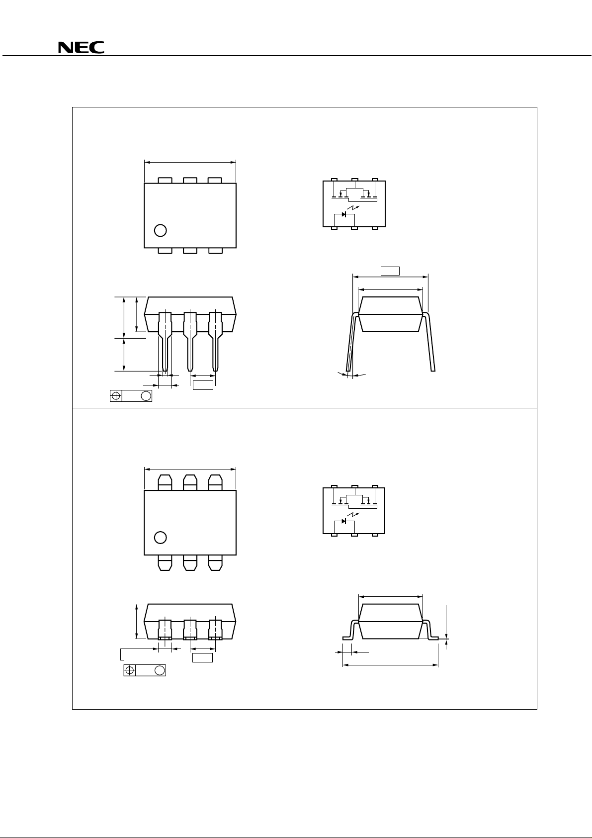
PACKAGE DIMENSIONS (in millimeters)
PS7341-1B,PS7341L-1B
PS7341-1B
4.15±0.3
3.3±0.3
0.5±0.1
1.34±0.1
0.25 M
3.5±0.3
9.25±0.5
2.54
PS7341L-1B
TOP VIEW
654
123
7.62
6.5±0.5
0 to 15˚
1. LED Anode
2. LED Cathode
3. NC
4. MOS FET Drain
5. MOS FET Source
6. MOS FET Drain
3.5±0.3
1.34±0.1
0.25 M
9.25±0.5
2.54
TOP VIEW
654
123
6.5±0.5
0.9±0.25
9.60±0.4
1. LED Anode
2. LED Cathode
3. NC
4. MOS FET Drain
5. MOS FET Source
6. MOS FET Drain
+0.10
–0.05
0.10
2
Data Sheet P14229EJ1V0DS00
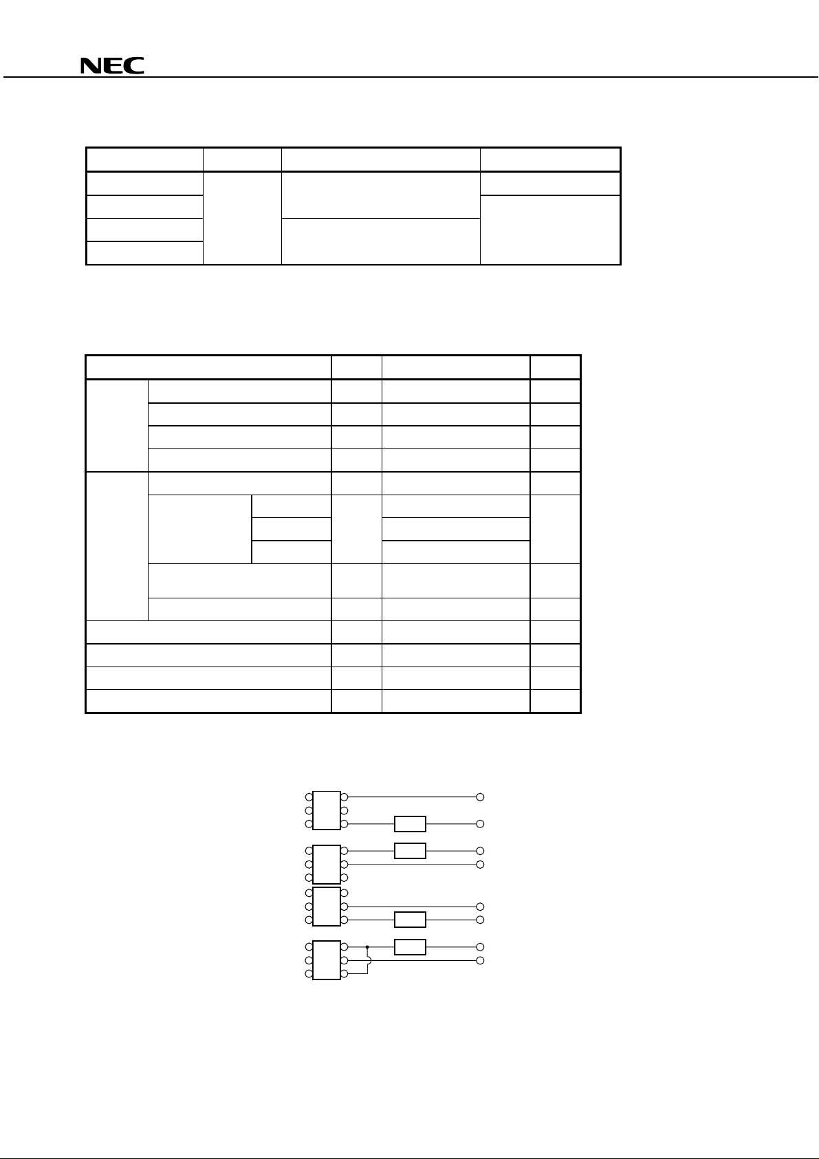
ORDERING INFORMATION
PS7341-1B,PS7341L-1B
Part Number Package Packing Style
Application Part Number
PS7341-1B 8-pin DIP Magazine case 50 pcs PS7341-1B
PS7341L-1B PS7341L-1B
PS7341L-1B-E3 Embossed Tape 1 000 pcs/reel
PS7341L-1B-E4
For the application of the Safety Standard, following part number should be used.
*1
ABSOLUTE MAXIMUM RATINGS (TA = 25 °°°°C, unless otherwise specified)
Parameter Symbol Ratings Unit
Diode Forward Current (DC) I
Reverse Voltage V
Power Dissipation P
Peak Forward Current
*1
MOS FET Break Down Voltage V
Continuous Connection A I
Load Current
*2
Connection B 200
Connection C 300
Pulse Load Current
*3
(AC/DC Connection)
Power Dissipation P
Isolation Voltage
*4
Total Power Dissipat i on P
Operating Ambient Temperature T
Storage Temperature T
F
R
D
FP
I
L
L
LP
I
D
50 mA
5.0 V
50 mW
1A
400 V
150 mA
300 mA
560 mW
BV 3 750 Vr.m.s.
T
A
stg
610 mW
−
40 to +85
−
40 to +125
°
C
°
C
*1
PW = 100
*1
Conditions: IF ≥ 2 mA. The following types of load connections are available.
*2
PW = 100 ms, 1shot
*3
AC voltage for 1 minute at T
*4
µ
s, Duty Cycle = 1 %
1
AV
25
3
1
2
B
1
2
3
1
2
C
3
A
= 25 °C, RH = 60 % between input and output
6
I
L
4
6
5
L
L
I
L
43
6
5
I
L
4
6
5
4
Data Sheet P14229EJ1V0DS00
L
I
L
L
IL + I
I
L
L
+
–
–
+
+
–
L
(AC/DC)
V
L
(DC)
L
(DC)
V
V
L
(DC)
3
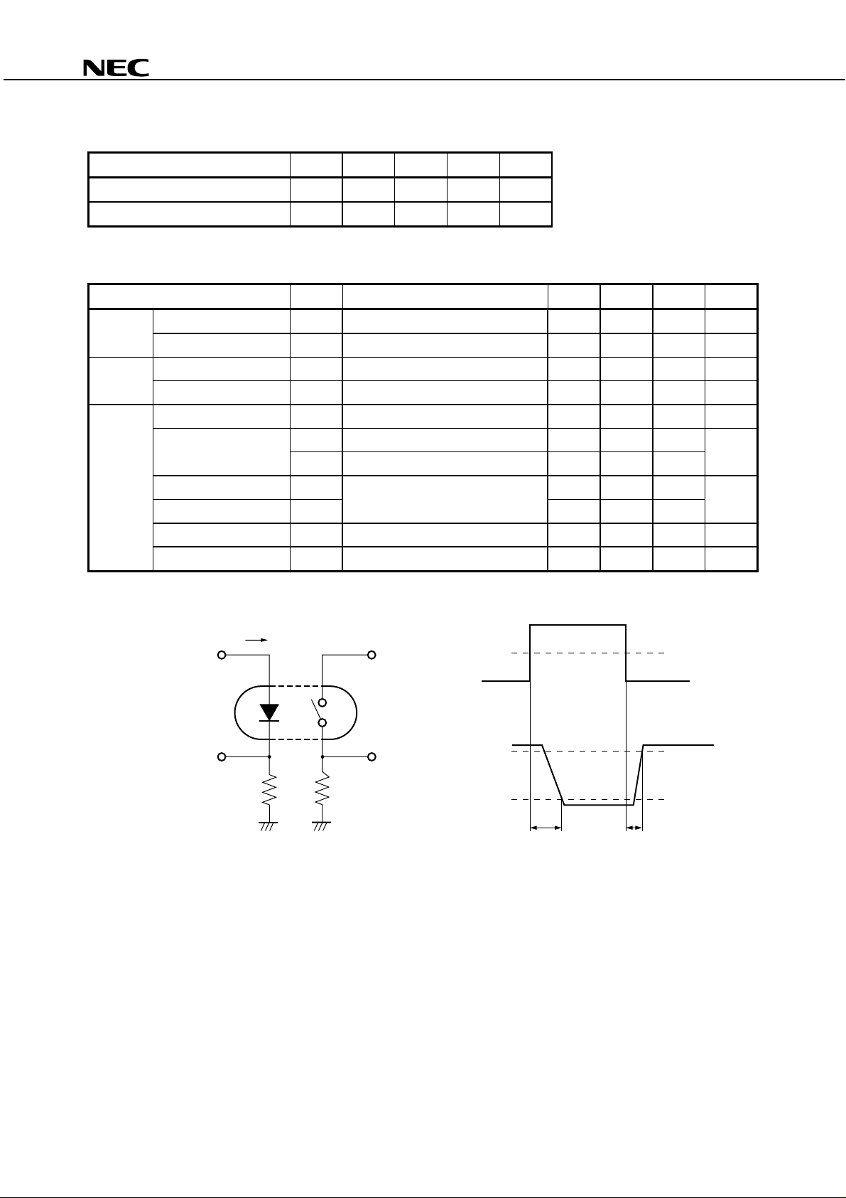
RECOMMENDED OPERATING CONDITIONS (TA = 25 °°°°C)
Parameter Symbol MIN. TYP. MAX. Unit
PS7341-1B,PS7341L-1B
LED Operating Current I
LED Off Voltage V
F
F
21020mA
00.5V
ELECTRICAL CHARACTERISTICS (TA = 25 °°°°C)
Parameter Symbol Conditions MIN. TYP. MAX. Unit
Diode Forward Voltage V
Reverse Current I
MOS FET Off-state Leakage Current I
Output Capacitance C
Coupled LED Off-state Current I
On-state Resistance R
Turn-on Time
Turn-off Time
*1
*1
Isolation Resistance R
Isolation Capacitance C
Test Circuit for Switching Time
*1
F
R
Loff
outIF
FoffIL
on1IF
on2IF
R
on
t
off
t
I-O
I-O
IF = 10 mA 1.2 1.4 V
VR = 5 V 5.0
IF = 10 mA, VD = 400 V 0.5 10
= 10 mA, VD = 0 V, f = 1 MHz 185 pF
= 150 mA 2.0 mA
= 0 mA, IL = 10 mA 20 30
= 0 mA, IL = 150 mA 16 25
IF = 10 mA, VO = 5 V, PW ≥ 10 ms 0.03 0.2 ms
I-O
V
= 1.0 kV
V = 0 V, f = 1 MHz 1.1 pF
µ
A
µ
A
Ω
0.6 1.5
DC
10
9
Ω
I
F
Pulse Input
Input monitor monitorV
R
in
R
L
V
L
Input
50 %
0
V
O
O
= 5 V
90 %
Output
10 %
t
off
t
on
4
Data Sheet P14229EJ1V0DS00
 Loading...