


Mitsubishi MH8S64BBKG-10L, MH8S64BBKG-8, MH8S64BBKG-8L, MH8S64BBKG-7, MH4S64BBKG-7L Datasheet
...Preliminary Spec. |
MITSUBISHI LSIs |
Some contents are subject to change without notice.
MH4S64BBKG -7,-7L,-8,-8L,-10,-10L
268435456-BIT (4194304 - WORD BY 64-BIT)SynchronousDRAM
DESCRIPTION
The MH4S64BBKG is 4194304 - word by 64-bit Synchronous DRAM module. This consists of four industry standard 4Mx16 Synchronous DRAMs in TSOP and one industory standard EEPROM in TSSOP.
The mounting of TSOP on a card edge Dual Inline package provides any application where high densities and large quantities of memory are required.
This is a socket type - memory modules, suitable for easy interchange or addition of modules.
FEATURES
|
Frequency |
CLK Access Time |
|
(Component SDRAM) |
|
|
|
|
-7,-7L |
100MHz |
6.0ns(CL=3) |
-8,-8L |
100MHz |
6.0ns(CL=3) |
|
|
|
-10,-10L |
100MHz |
8.0ns(CL=3) |
|
|
|
PC100 compliant
 Utilizes industry standard 4M x 16 Synchronous DRAMs TSOP and industry standard EEPROM in TSSOP
 144-pin (72-pin dual in-line package)
 single 3.3V±0.3V power supply
 Clock frequency 100MHz(max.)
 Fully synchronous operation referenced to clock rising edge
 4 bank operation controlled by BA0,1(Bank Address)
 /CAS latency- 2/3(programmable)
 Burst length- 1/2/4/8/Full Page(programmable)
 Burst typesequential / interleave(programmable)
 Column access - random
 Auto precharge / All bank precharge controlled by A10
 Auto refresh and Self refresh
 4096 refresh cycle /64ms
 LVTTL Interface
APPLICATION
main memory or graphic memory in computer systems
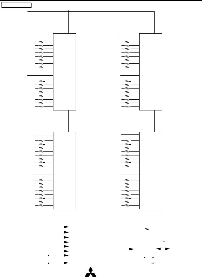
PCB Outline
|
|
|
|
|
|
|
|
|
|
|
|
|
|
|
|
|
|
|
|
|
|
|
|
|
|
|
|
|
|
|
|
|
|
|
|
|
|
|
|
|
|
|
|
|
|
|
|
|
|
|
|
|
|
|
|
|
|
|
|
|
|
|
|
|
|
|
|
|
|
|
|
|
|
|
|
|
|
|
|
|
|
|
|
|
|
|
|
|
|
|
|
|
|
|
|
|
|
|
|
|
|
|
|
|
|
|
|
|
|
|
|
|
|
|
|
|
|
|
|
|
|
|
|
|
|
|
|
|
|
|
|
|
|
|
|
|
|
|
|
|
|
|
|
|
|
|
|
|
|
|
|
|
|
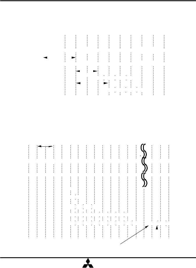
(Front) |
1 |
|
|
|
|
|
|
|
|
|
|
|
|
|
|
|
|
|
|
|
|
|
|
|
|
|
|
|
|
143 |
||||||||||||||||||||||||||||||||||||||||||||||
(Back) |
2 |
|
|
|
|
|
|
|
|
|
|
|
|
|
|
|
|
|
|
|
|
|
|
|
|
|
|
|
|
144 |
||||||||||||||||||||||||||||||||||||||||||||||
MIT-DS-0295-0.0
MITSUBISHI |
22.Dec.1998 |
ELECTRIC
( 1 / 55 )

Preliminary Spec. |
MITSUBISHI LSIs |
Some contents are subject to change without notice.
MH4S64BBKG -7,-7L,-8,-8L,-10,-10L
268435456-BIT (4194304 - WORD BY 64-BIT)SynchronousDRAM
PIN CONFIGURATION
|
PIN |
Front side |
PIN |
Back side |
PIN |
Front side |
PIN |
Back side |
|
|
Number |
Pin Name |
Number |
Pin Name |
Number |
Pin Name |
Number |
Pin Name |
|
|
1 |
Vss |
2 |
Vss |
73 |
NC |
74 |
CLK1 |
|
|
3 |
DQ0 |
4 |
DQ32 |
75 |
Vss |
76 |
Vss |
|
|
5 |
DQ1 |
6 |
DQ33 |
77 |
NC |
78 |
NC |
|
|
7 |
DQ2 |
8 |
DQ34 |
79 |
NC |
80 |
NC |
|
|
9 |
DQ3 |
10 |
DQ35 |
81 |
Vcc |
82 |
Vcc |
|
|
11 |
Vcc |
12 |
Vcc |
83 |
DQ16 |
84 |
DQ48 |
|
|
13 |
DQ4 |
14 |
DQ36 |
85 |
DQ17 |
86 |
DQ49 |
|
|
15 |
DQ5 |
16 |
DQ37 |
87 |
DQ18 |
88 |
DQ50 |
|
|
17 |
DQ6 |
18 |
DQ38 |
89 |
DQ19 |
90 |
DQ51 |
|
|
19 |
DQ7 |
20 |
DQ39 |
91 |
Vss |
92 |
Vss |
|
|
21 |
Vss |
22 |
Vss |
93 |
DQ20 |
94 |
DQ52 |
|
|
23 |
DQMB0 |
24 |
DQMB4 |
95 |
DQ21 |
96 |
DQ53 |
|
|
25 |
DQMB1 |
26 |
DQMB5 |
97 |
DQ22 |
98 |
DQ54 |
|
|
27 |
Vcc |
28 |
Vcc |
99 |
DQ23 |
100 |
DQ55 |
|
|
29 |
A0 |
30 |
A3 |
101 |
Vcc |
102 |
Vcc |
|
|
31 |
A1 |
32 |
A4 |
103 |
A6 |
104 |
A7 |
|
|
33 |
A2 |
34 |
A5 |
105 |
A8 |
106 |
BA0 |
|
|
35 |
Vss |
36 |
Vss |
107 |
Vss |
108 |
Vss |
|
|
37 |
DQ8 |
38 |
DQ40 |
109 |
A9 |
110 |
BA1 |
|
|
39 |
DQ9 |
40 |
DQ41 |
111 |
A10 |
112 |
A11 |
|
|
|
|
|
|
|
|
|
|
|
|
41 |
DQ10 |
42 |
DQ42 |
113 |
Vcc |
114 |
Vcc |
|
|
|
|
|
|
|
|
|
|
|
|
43 |
DQ11 |
44 |
DQ43 |
115 |
DQMB2 |
116 |
DQMB6 |
|
|
45 |
Vcc |
46 |
Vcc |
117 |
DQMB3 |
118 |
DQMB7 |
|
|
47 |
DQ12 |
48 |
DQ44 |
119 |
Vss |
120 |
Vss |
|
|
|
|
|
|
|
|
|
|
|
|
49 |
DQ13 |
50 |
DQ45 |
121 |
DQ24 |
122 |
DQ56 |
|
|
|
|
|
|
|
|
|
|
|
|
51 |
DQ14 |
52 |
DQ46 |
123 |
DQ25 |
124 |
DQ57 |
|
|
|
|
|
|
|
|
|
|
|
|
53 |
DQ15 |
54 |
DQ47 |
125 |
DQ26 |
126 |
DQ58 |
|
|
55 |
Vss |
56 |
Vss |
127 |
DQ27 |
128 |
DQ59 |
|
|
|
|
|
|
|
|
|
|
|
|
57 |
NC |
58 |
NC |
129 |
Vcc |
130 |
Vcc |
|
|
|
|
|
|
|
|
|
|
|
|
59 |
NC |
60 |
NC |
131 |
DQ28 |
132 |
DQ60 |
|
|
|
|
|
|
|
|
|
|
|
|
61 |
CLK0 |
62 |
CKE0 |
133 |
DQ29 |
134 |
DQ61 |
|
|
|
|
|
|
|
|
|
|
|
|
63 |
Vcc |
64 |
Vcc |
135 |
DQ30 |
136 |
DQ62 |
|
|
|
|
|
|
|
|
|
|
|
|
65 |
/RAS |
66 |
/CAS |
137 |
DQ31 |
138 |
DQ63 |
|
|
|
|
|
|
|
|
|
|
|
|
67 |
/WE |
68 |
NC |
139 |
Vss |
140 |
Vss |
|
|
69 |
/S0 |
70 |
NC |
141 |
SDA |
142 |
SCL |
|
|
71 |
NC |
72 |
NC |
143 |
Vcc |
144 |
Vcc |
|
NC = No Connection
MIT-DS-0295-0.0
MITSUBISHI |
22.Dec.1998 |
ELECTRIC
( 2 / 55 )
Preliminary Spec. |
MITSUBISHI LSIs |
Some contents are subject to change without notice.
MH4S64BBKG -7,-7L,-8,-8L,-10,-10L
268435456-BIT (4194304 - WORD BY 64-BIT)SynchronousDRAM
Block Diagram 

/S0
DQMB0 |
DQML /CS |
DQMB4 |
DQML /CS |
|||
DQ0 |
I/O 0 |
|
DQ32 |
I/O 0 |
|
|
DQ1 |
I/O 1 |
D0 |
DQ33 |
I/O 1 |
D2 |
|
DQ2 |
I/O 2 |
DQ34 |
I/O 2 |
|||
|
|
|||||
DQ3 |
I/O 3 |
|
DQ35 |
I/O 3 |
|
|
DQ4 |
I/O 4 |
|
DQ36 |
I/O 4 |
|
|
DQ5 |
I/O 5 |
|
DQ37 |
I/O 5 |
|
|
DQ6 |
I/O 6 |
|
DQ38 |
I/O 6 |
|
|
DQ7 |
I/O 7 |
|
DQ39 |
I/O 7 |
|
|
DQMB1 |
DQMU |
|
DQMB5 |
DQMU |
|
|
DQ8 |
I/O 8 |
|
DQ40 |
I/O 8 |
|
|
DQ9 |
I/O 9 |
|
DQ41 |
I/O 9 |
|
|
DQ10 |
I/O 10 |
|
DQ42 |
I/O 10 |
|
|
DQ11 |
I/O 11 |
|
DQ43 |
I/O 11 |
|
|
DQ12 |
I/O 12 |
|
DQ44 |
I/O 12 |
|
|
DQ13 |
I/O 13 |
|
DQ45 |
I/O 13 |
|
|
DQ14 |
I/O 14 |
|
DQ46 |
I/O 14 |
|
|
DQ15 |
I/O 15 |
|
DQ47 |
I/O 15 |
|
|
DQMB2 |
|
DQML |
/CS |
DQ16 |
|
I/O 0 |
|
DQ17 |
|
I/O 1 |
D1 |
DQ18 |
|
I/O 2 |
|
|
|
||
DQ19 |
|
I/O 3 |
|
DQ20 |
|
I/O 4 |
|
DQ21 |
|
I/O 5 |
|
DQ22 |
|
I/O 6 |
|
DQ23 |
|
I/O 7 |
|
DQMB3 |
|
DQMU |
|
DQ24 |
|
I/O 8 |
|
DQ25 |
|
I/O 9 |
|
DQ26 |
|
I/O 10 |
|
DQ27 |
|
I/O 11 |
|
DQ28 |
|
I/O 12 |
|
DQ29 |
|
I/O 13 |
|
DQ30 |
|
I/O 14 |
|
DQ31 |
10Ω |
I/O 15 |
|
|
|
|
DQMB6 |
DQML /CS |
||
DQ48 |
I/O 0 |
|
|
DQ49 |
I/O 1 |
D3 |
|
DQ50 |
I/O 2 |
||
|
|||
DQ51 |
I/O 3 |
|
|
DQ52 |
I/O 4 |
|
|
DQ53 |
I/O 5 |
|
|
DQ54 |
I/O 6 |
|
|
DQ55 |
I/O 7 |
|
|
DQMB7 |
DQMU |
|
|
DQ56 |
I/O 8 |
|
|
DQ57 |
I/O 9 |
|
|
DQ58 |
I/O 10 |
|
|
DQ59 |
I/O 11 |
|
|
DQ60 |
I/O 12 |
|
|
DQ61 |
I/O 13 |
|
|
DQ62 |
I/O 14 |
|
|
DQ63 |
I/O 15 |
|
|
|
CLK0 |
|
|
|
D0 - D3 |
|
|
CLK1 |
|
|
|
|
|
|
|
|
|
|
|
|
|
|||||||
|
|
|
|
|
|
|
|
|
|
|
|
|
|
|
|
|
|
|||||||||||
|
CKE0 |
|
|
|
|
|
|
D0 - D3 |
|
|
10Ω |
|
|
|
|
|
|
|
|
10pF |
||||||||
|
|
|
|
|
|
|
|
|
|
|
|
|
|
|
|
|
||||||||||||
|
|
|
|
|
|
|
|
|
|
|
||||||||||||||||||
|
/RAS |
|
|
|
|
|
|
|
D0 - D3 |
|
|
|
|
|
|
|
|
|
|
|
|
|
|
|
|
|
|
|
|
|
|
|
|
|
|
|
|
|
|
|
|
|
|
|
|
|
|
|
|
|
|
|
|
|
|||
|
|
|
|
|
|
|
|
|
|
|
|
|
|
|
|
|
|
|
|
|
||||||||
|
/CAS |
|
|
D0 - D3 |
|
|
|
|
|
|
|
|
|
|
|
|
|
|
|
|
|
|
||||||
|
|
|
|
|
|
|
|
|
|
|
SERIAL PD |
|||||||||||||||||
|
|
|
|
|
|
|||||||||||||||||||||||
|
/WE |
|
|
D0 - D3 |
|
|
|
|||||||||||||||||||||
|
|
|
|
|
|
|||||||||||||||||||||||
BA0,BA1,A<11:0> |
|
|
|
|
|
|
|
D0 - D3 |
SCL |
|
|
A0 A1 |
A2 |
|
|
|
|
SDA |
||||||||||
|
|
|
|
|
|
|
|
|
|
|
|
|
||||||||||||||||
|
|
|
|
|
|
|
|
|
|
|
||||||||||||||||||
|
Vcc |
|
|
|
|
|
|
|
|
D0 - D3 |
|
|
|
|
|
|
|
|
|
|
|
|
|
|
|
|
|
|
|
|
|
|
|
|
|
|
|
|
|
|
|
|
|
|
|
|
|
|
|
|
|
|
|
|
|||
|
Vss |
|
|
|
|
|
|
|
|
D0 - D3 |
|
|
|
|
|
|
|
|
|
|
|
|
|
|
|
|
|
|
|
|
|
|
|
|
|
|
|
|
|
|
|
|
|
|
|
|
|
|
|
|
|
|
|
|
|
||
|
|
|
|
|
|
|
|
|
|
|
|
|
|
|
|
|
|
|
|
|
|
|
|
|
|
|
||
|
|
|
|
|
|
|
|
|
|
|
|
|
|
|
|
|
|
|
|
|
|
|
|
|
|
|
||
|
|
|
|
|
|
|
|
|
|
|
|
|
|
|
|
|
|
|
|
|
|
|
|
|
|
|||
|
|
|
|
|
|
|
|
|
|
|
|
|
|
|
|
|
|
|
|
|
|
|
|
|
|
|
|
|
|
MIT-DS-0295-0.0 |
|
|
MITSUBISHI |
|
|
|
|
|
|
|
|
|
|
|
|
|
|
22.Dec.1998 |
|||||||||
|
|
|
|
|
|
|
|
|
|
|
ELECTRIC |
|
|
|
|
|
|
|
|
|
|
|
|
|
|
|
|
|
( 3 / 55 )

Preliminary Spec. |
MITSUBISHI LSIs |
Some contents are subject to change without notice.
MH4S64BBKG -7,-7L,-8,-8L,-10,-10L
268435456-BIT (4194304 - WORD BY 64-BIT)SynchronousDRAM
Serial Presence Detect Table I
|
Byte |
Function described |
|
|
|
SPD enrty data |
|
SPD DATA(hex) |
|
|
|
|
|
|
|
|
|
|
|
0 |
Defines # bytes written into serial memory at module mfgr |
128 |
|
80 |
|
||||
|
|
|
|
|
|
|
|
|
|
1 |
Total # bytes of SPD memory device |
|
|
|
256 Bytes |
08 |
|
||
|
|
|
|
|
|
|
|
|
|
2 |
Fundamental memory type |
|
|
|
SDRAM |
04 |
|
||
|
|
|
|
|
|
|
|
|
|
3 |
# Row Addresses on this assembly |
|
|
|
A0-A11 |
0C |
|||
|
|
|
|
|
|
|
|
|
|
4 |
# Column Addresses on this assembly |
|
|
|
A0-A7 |
08 |
|
||
|
|
|
|
|
|
|
|
|
|
5 |
# Module Banks on this assembly |
|
|
|
1BANK |
01 |
|
||
|
|
|
|
|
|
|
|
|
|
6 |
Data Width of this assembly... |
|
|
|
x64 |
40 |
|
||
|
|
|
|
|
|
|
|
|
|
7 |
... Data Width continuation |
|
|
|
0 |
|
00 |
|
|
|
|
|
|
|
|
|
|
|
|
8 |
Voltage interface standard of this assembly |
|
LVTTL |
01 |
|
||||
|
|
|
|
|
|
|
|
|
|
9 |
SDRAM Cycletime at Max. Supported CAS Latency (CL). |
|
10ns |
A0 |
|||||
|
|
Cycle time for CL=3 |
|
|
|
||||
|
|
|
|
|
|
|
|
|
|
|
|
|
|
|
|
|
|
|
|
10 |
SDRAM Access from Clock |
-7,7L,-8,8L |
6ns |
60 |
|
||||
|
|
|
|
|
|
|
|
|
|
|
|
tAC for CL=3 |
|
|
-10,10L |
8ns |
80 |
|
|
|
|
|
|
|
|
|
|
|
|
11 |
DIMM Configuration type (Non-parity,Parity,ECC) |
Non-PARITY |
00 |
|
|||||
|
|
|
|
|
|
|
|
|
|
12 |
Refresh Rate/Type |
|
|
|
self refresh(15.625uS) |
80 |
|
||
|
|
|
|
|
|
|
|
|
|
13 |
SDRAM width,Primary DRAM |
|
|
|
x16 |
10 |
|
||
|
|
|
|
|
|
|
|
|
|
14 |
Error Checking SDRAM data width |
|
|
|
N/A |
00 |
|
||
|
|
|
|
|
|
|
|
|
|
15 |
Minimum Clock Delay,Back to Back Random Column Addresses |
1 |
|
01 |
|
||||
|
|
|
|
|
|
|
|
|
|
16 |
Burst Lengths Supported |
|
|
|
1/2/4/8/Full page |
8F |
|||
|
|
|
|
|
|
|
|
|
|
17 |
# Banks on Each SDRAM device |
|
|
|
4bank |
04 |
|
||
|
|
|
|
|
|
|
|
|
|
18 |
CAS# Latency |
|
|
|
2/3 |
|
06 |
|
|
|
|
|
|
|
|
|
|
|
|
19 |
CS# Latency |
|
|
|
0 |
|
01 |
|
|
20 |
Write Latency |
|
|
|
0 |
|
01 |
|
|
21 |
SDRAM Module Attributes |
|
|
|
non-buffered,non-registered |
|
00 |
|
|
22 |
SDRAM Device Attributes:General |
|
|
|
Precharge All,Auto precharge |
|
0E |
|
|
23 |
SDRAM Cycle time(2nd highest CAS latency) |
-7,7L |
10ns |
|
A0 |
|
|||
|
|
Cycle time for CL=2 |
|
|
-8,8L |
13ns |
|
D0 |
|
|
|
|
|
|
-10,10L |
15ns |
|
F0 |
|
24 |
SDRAM Access form Clock(2nd highest CAS latency) |
-7,7L |
6ns |
60 |
|
||||
|
|
tAC for CL=2 |
|
|
|
|
|
|
|
|
|
|
|
-8,8L |
7ns |
|
70 |
|
|
|
|
|
|
|
-10,10L |
8ns |
|
80 |
|
25 |
SDRAM Cycle time(3rd highest CAS latency) |
|
N/A |
|
00 |
|
|||
|
26 |
SDRAM Access form Clock(3rd highest CAS latency) |
|
N/A |
|
00 |
|
||
27 |
Precharge to Active Minimum |
-7,7L,-8,8L |
20ns |
|
14 |
|
|||
|
|
|
|
|
-10,10L |
30ns |
|
1E |
|
28 |
Row Active to Row Active Min. |
|
|
|
20ns |
|
14 |
|
|
29 |
RAS to CAS Delay Min |
-7,7L,-8,8L |
20ns |
|
14 |
|
|||
|
|
|
|
|
-10,10L |
30ns |
|
1E |
|
30 |
Active to Precharge Min |
-7,7L,-8,8L |
50ns |
32 |
|
||||
|
|
|
|
|
|
|
|
|
|
|
|
|
|
|
-10,10L |
60ns |
|
3C |
|
MIT-DS-0295-0.0
MITSUBISHI |
22.Dec.1998 |
ELECTRIC
( 4 / 55 )

Preliminary Spec. |
MITSUBISHI LSIs |
Some contents are subject to change without notice.
MH4S64BBKG -7,-7L,-8,-8L,-10,-10L
268435456-BIT (4194304 - WORD BY 64-BIT)SynchronousDRAM
Serial Presence Detect Table II
31 |
|
Density of each bank on module |
|
32MByte |
|
08 |
|
|
|
|
|||||
32 |
|
Command and Address signal input setup time |
-7,7L,-8,8L |
2ns |
20 |
|
|
|
|
|
|
|
|
|
|
|
|
|
-10,10L |
N/A |
00 |
|
|
|
|
|
|
|
|
|
|
33 |
|
Command and Address signal input hold time |
-7,7L,-8,8L |
1ns |
|
10 |
|
|
|
|
-10,10L |
N/A |
00 |
|
|
34 |
|
Data signal input setup time |
-7,7L,-8,8L |
2ns |
20 |
|
|
|
|
|
-10,10L |
N/A |
00 |
|
|
35 |
|
Data signal input hold time |
-7,7L,-8,8L |
1ns |
10 |
|
|
|
|
|
-10,10L |
N/A |
|
00 |
|
36-61 |
|
Superset Information (may be used in future) |
option |
|
00 |
|
|
62 |
|
SPD Revision |
-7,7L,-8,8L |
rev 1.2A |
|
12 |
|
|
|
|
-10,10L |
rev 1 |
|
01 |
|
63 |
|
Checksum for bytes 0-62 |
|
Check sum for -7,7L |
|
04 |
|
|
|
|
|
Check sum for -8,-8L |
44 |
|
|
|
|
|
|
Check sum for -10,-10L |
|
41 |
|
64-71 |
|
Manufactures Jedec ID code per JEP-108E |
MITSUBISHI |
1CFFFFFFFFFFFFFF |
|||
|
|
|
|
|
|
|
|
72 |
|
Manufacturing location |
|
Miyoshi,Japan |
01 |
|
|
|
|
|
|
|
|
|
|
|
|
|
|
Tajima,Japan |
|
02 |
|
|
|
|
|
NC,USA |
03 |
|
|
|
|
|
|
|
|
|
|
|
|
|
|
Germany |
04 |
|
|
|
|
|
|
|
|
|
|
73-90 |
|
Manufactures Part Number |
|
MH4S64BBKG-7 |
|
4D483453363442424B472D374C2020202020 |
|
|
|
|
|
MH4S64BBKG-7L |
|
4D483453363442424B472D37202020202020 |
|
|
|
|
|
MH4S64BBKG-8 |
4D483453363442424B472D38202020202020 |
||
|
|
|
|
MH4S64BBKG-8L |
4D483453363442424B472D384C2020202020 |
||
|
|
|
|
|
|
||
|
|
|
|
MH4S64BBKG-10 |
4D483453363442424B472D31302020202020 |
||
|
|
|
|
|
|
||
|
|
|
|
MH4S64BBKG-10L |
|
4D483453363442424B472D31304C20202020 |
|
91-92 |
|
Revision Code |
|
PCB revision |
rrrr |
||
|
|
|
|
|
|
|
|
93-94 |
|
Manufacturing date |
|
year/week code |
|
yyww |
|
95-98 |
|
Assembly Serial Number |
|
serial number |
ssssssss |
||
|
|
|
|
|
|
|
|
99-125 |
|
Manufacture Specific Data |
|
option |
00 |
|
|
|
|
|
|
|
|
|
|
126 |
|
Intetl specification frequency |
-7,7L-8,8L |
100MHz |
|
64 |
|
|
|
|
-10,10L |
66MHz |
|
66 |
|
127 |
|
Intel specification CAS# Latency support |
-7,7L |
|
|
8F |
|
|
|
|
|
|
|
|
|
|
|
|
-8,8L |
|
|
8D |
|
|
|
|
|
|
|
|
|
|
|
|
-10,10L |
|
|
06 |
|
|
|
|
|
|
|
|
|
128+ |
|
Unused storage locations |
|
open |
00 |
|
|
|
|
|
|
|
|
|
|
MIT-DS-0295-0.0
MITSUBISHI |
22.Dec.1998 |
ELECTRIC
( 5 / 55 )

Preliminary Spec. |
MITSUBISHI LSIs |
Some contents are subject to change without notice.
MH4S64BBKG -7,-7L,-8,-8L,-10,-10L
|
|
|
268435456-BIT (4194304 - WORD BY 64-BIT)SynchronousDRAM |
|
|
|
|
|
|
|
PIN FUNCTION |
|
|
|
|
|
|
|
|
|
CLK |
Input |
Master Clock:All other inputs are referenced to the rising |
|
|
(CLK0 ~ CLK1) |
edge of CK |
||
|
|
|||
|
|
|
|
|
|
|
|
Clock Enable:CKE controls internal clock.When CKE is |
|
|
|
|
low,internal clock for the following cycle is ceased. CKE is |
|
|
CKE0 |
Input |
also used to select auto / self refresh. After self refresh |
|
|
|
|
mode is started, CKE E becomes asynchronous input.Self |
|
|
|
|
refresh is maintained as long as CKE is low. |
|
|
|
|
|
|
|
/S0 |
Input |
Chip Select: When /S is high,any command means |
|
|
No Operation. |
|||
|
|
|
||
|
|
|
|
|
|
/RAS,/CAS,/WE |
Input |
Combination of /RAS,/CAS,/WE defines basic commands. |
|
|
|
|
|
|
|
|
|
A0-11 specify the Row/Column Address in conjunction with |
|
|
|
|
BA0,1.The Row Address is specified by A0-11.The Column |
|
|
A0-11 |
Input |
Address is specified by A0-7.A10 is also used to indicate |
|
|
precharge option.When A10 is high at a read / write |
|||
|
|
|
||
|
|
|
command, an auto precharge is performed. When A10 is |
|
|
|
|
high at a precharge command, both banks are precharged. |
|
|
|
|
|
|
|
|
|
Bank Address:BA0,1 is not simply BA.BA specifies the |
|
|
BA0,1 |
Input |
bank to which a command is applied.BA0,1 must be set |
|
|
|
|
with ACT,PRE,READ,WRITE commands |
|
|
|
|
|
|
|
DQ0-63 |
Input/Output |
Data In and Data out are referenced to the rising edge of |
|
|
|
|
CK |
|
|
|
|
|
|
|
|
|
Din Mask/Output Disable:When DQMB is high in burst |
|
|
DQMB0-7 |
Input |
write.Din for the current cycle is masked.When DQMB is high |
|
|
|
|
in burst read,Dout is disabled at the next but one cycle. |
|
|
|
|
|
|
|
Vdd,Vss |
Power Supply |
Power Supply for the memory mounted module. |
|
|
|
|
|
|
|
SCL |
Input |
Serial clock for serial PD |
|
|
|
|
|
|
|
SDA |
Output |
Serial data for serial PD |
|
|
|
|
|
|
MIT-DS-0295-0.0
MITSUBISHI |
22.Dec.1998 |
ELECTRIC
( 6 / 55 )
Preliminary Spec. |
MITSUBISHI LSIs |
Some contents are subject to change without notice.
MH4S64BBKG -7,-7L,-8,-8L,-10,-10L
268435456-BIT (4194304 - WORD BY 64-BIT)SynchronousDRAM
BASIC FUNCTIONS
The MH4S64BBKG provides basic functions,bank(row)activate,burst read / write, bank(row)precharge,and auto / self refresh.
Each command is defined by control signals of /RAS,/CAS and /WE at CK rising edge. In addition to 3 signals,/S,CKE and A10 are used as chip select,refresh option,and precharge option,respectively.
To know the detailed definition of commands please see the command truth table.
CK
/S
/RAS 


/CAS 


/WE
CKE 


A10
Chip Select : L=select, H=deselect
Command
Command |
define basic commands |
Command
Refresh Option @refresh command
Precharge Option @precharge or read/write command
Activate(ACT) [/RAS =L, /CAS = /WE =H]
ACT command activates a row in an idle bank indicated by BA.
Read(READ) [/RAS =H,/CAS =L, /WE =H]
READ command starts burst read from the active bank indicated by BA.First output data appears after /CAS latency. When A10 =H at this command,the bank is deactivated after the burst read(auto-precharge,READA).
Write(WRITE) [/RAS =H, /CAS = /WE =L]
WRITE command starts burst write to the active bank indicated by BA. Total data length to be written is set by burst length. When A10 =H at this command, the bank is deactivated after the burst write(auto-precharge,WRITEA).
Precharge(PRE) [/RAS =L, /CAS =H,/WE =L]
PRE command deactivates the active bank indicated by BA. This command also terminates burst read / write operation. When A10 =H at this command, both banks are deactivated(precharge all, PREA).
Auto-Refresh(REFA) [/RAS =/CAS =L, /WE =CKE =H]
PEFA command starts auto-refresh cycle. Refresh address including bank address are generated internally. After this command, the banks are precharged automatically.
MIT-DS-0295-0.0
MITSUBISHI |
22.Dec.1998 |
ELECTRIC
( 7 / 55 )

Preliminary Spec. |
MITSUBISHI LSIs |
Some contents are subject to change without notice.
MH4S64BBKG -7,-7L,-8,-8L,-10,-10L
268435456-BIT (4194304 - WORD BY 64-BIT)SynchronousDRAM
COMMAND TRUTH TABLE
COMMAND |
MNEMONIC |
CKE |
CKE |
/S |
/RAS |
/CAS |
/WE |
BA0,1 |
A11 |
A10 |
A0-9 |
|
|
|
n-1 |
n |
|
|
|
|
|
|
|
|
|
Deselect |
DESEL |
H |
X |
H |
X |
X |
X |
X |
X |
X |
X |
|
No Operation |
NOP |
H |
X |
L |
H |
H |
H |
X |
X |
X |
X |
|
Row Adress Entry & |
ACT |
H |
X |
L |
L |
H |
H |
V |
V |
V |
V |
|
Bank Activate |
|
|||||||||||
|
|
|
|
|
|
|
|
|
|
|
|
|
|
|
|
|
|
|
|
|
|
|
|
|
|
Single Bank Precharge |
PRE |
H |
X |
L |
L |
H |
L |
V |
X |
L |
X |
|
Precharge All Bank |
PREA |
H |
X |
L |
L |
H |
L |
X |
X |
H |
X |
|
|
|
|
|
|
|
|
|
|
|
|
|
|
Column Address Entry |
WRITE |
H |
X |
L |
H |
L |
L |
V |
X |
L |
V |
|
& Write |
|
|||||||||||
|
|
|
|
|
|
|
|
|
|
|
|
|
|
|
|
|
|
|
|
|
|
|
|
|
|
Column Address Entry |
|
|
|
|
|
|
|
|
|
|
|
|
& Write with Auto- |
WRITEA |
H |
X |
L |
H |
L |
L |
V |
X |
H |
V |
|
Precharge |
|
|
|
|
|
|
|
|
|
|
|
|
|
|
|
|
|
|
|
|
|
|
|
|
|
Column Address Entry |
READ |
H |
X |
L |
H |
L |
H |
V |
X |
L |
V |
|
& Read |
|
|||||||||||
|
|
|
|
|
|
|
|
|
|
|
|
|
|
|
|
|
|
|
|
|
|
|
|
|
|
Column Address Entry |
|
|
|
|
|
|
|
|
|
|
|
|
& Read with Auto |
READA |
H |
X |
L |
H |
L |
H |
V |
X |
H |
V |
|
Precharge |
|
|
|
|
|
|
|
|
|
|
|
|
|
|
|
|
|
|
|
|
|
|
|
|
|
Auto-Refresh |
REFA |
H |
H |
L |
L |
L |
H |
X |
X |
X |
X |
|
|
|
|
|
|
|
|
|
|
|
|
|
|
Self-Refresh Entry |
REFS |
H |
L |
L |
L |
L |
H |
X |
X |
X |
X |
|
Self-Refresh Exit |
REFSX |
L |
H |
H |
X |
X |
X |
X |
X |
X |
X |
|
|
|
L |
H |
L |
H |
H |
H |
X |
X |
X |
X |
|
|
|
|
|
|
|
|
|
|
|
|
|
|
Burst Terminate |
TERM |
H |
X |
L |
H |
H |
L |
X |
X |
X |
X |
|
Mode Register Set |
MRS |
H |
X |
L |
L |
L |
L |
L |
L |
L |
V*1 |
|
H =High Level, L = Low Level, V = Valid, X = Don't Care, n = CK cycle number
NOTE:
1.A7-9 = 0, A0-6 = Mode Address
MIT-DS-0295-0.0
MITSUBISHI |
22.Dec.1998 |
ELECTRIC
( 8 / 55 )

Preliminary Spec. |
MITSUBISHI LSIs |
Some contents are subject to change without notice.
MH4S64BBKG -7,-7L,-8,-8L,-10,-10L
268435456-BIT (4194304 - WORD BY 64-BIT)SynchronousDRAM
FUNCTION TRUTH TABLE
Current State |
/S |
/RAS |
/CAS |
/WE |
Address |
Command |
Action |
|
|
|
|
|
|
|
|
IDLE |
H |
X |
X |
X |
X |
DESEL |
NOP |
|
|
|
|
|
|
|
|
|
L |
H |
H |
H |
X |
NOP |
NOP |
|
|
|
|
|
|
|
|
|
L |
H |
H |
L |
BA |
TBST |
ILLEGAL*2 |
|
|
|
|
|
|
|
|
|
L |
H |
L |
X |
BA,CA,A10 |
READ/WRITE |
ILLEGAL*2 |
|
|
|
|
|
|
|
|
|
L |
L |
H |
H |
BA,RA |
ACT |
Bank Active,Latch RA |
|
|
|
|
|
|
|
|
|
L |
L |
H |
L |
BA,A10 |
PRE/PREA |
NOP*4 |
|
|
|
|
|
|
|
|
|
L |
L |
L |
H |
X |
REFA |
Auto-Refresh*5 |
|
|
|
|
|
|
|
|
|
L |
L |
L |
L |
Op-Code, |
MRS |
Mode Register Set*5 |
|
Mode-Add |
||||||
|
|
|
|
|
|
|
|
|
|
|
|
|
|
|
|
ROW ACTIVE |
H |
X |
X |
X |
X |
DESEL |
NOP |
|
|
|
|
|
|
|
|
|
L |
H |
H |
H |
X |
NOP |
NOP |
|
|
|
|
|
|
|
|
|
L |
H |
H |
L |
BA |
TBST |
NOP |
|
|
|
|
|
|
|
|
|
L |
H |
L |
H |
BA,CA,A10 |
READ/READA |
Begin Read,Latch CA, |
|
Determine Auto-Precharge |
||||||
|
|
|
|
|
|
|
|
|
|
|
|
|
|
|
|
|
L |
H |
L |
L |
BA,CA,A10 |
WRITE/ |
Begin Write,Latch CA, |
|
WRITEA |
Determine Auto-Precharge |
|||||
|
|
|
|
|
|
||
|
|
|
|
|
|
|
|
|
L |
L |
H |
H |
BA,RA |
ACT |
Bank Active/ILLEGAL*2 |
|
|
|
|
|
|
|
|
|
L |
L |
H |
L |
BA,A10 |
PRE/PREA |
Precharge/Precharge All |
|
|
|
|
|
|
|
|
|
L |
L |
L |
H |
X |
REFA |
ILLEGAL |
|
|
|
|
|
|
|
|
|
L |
L |
L |
L |
Op-Code, |
MRS |
ILLEGAL |
|
Mode-Add |
||||||
|
|
|
|
|
|
|
|
|
|
|
|
|
|
|
|
READ |
H |
X |
X |
X |
X |
DESEL |
NOP(Continue Burst to END) |
|
|
|
|
|
|
|
|
|
L |
H |
H |
H |
X |
NOP |
NOP(Continue Burst to END) |
|
|
|
|
|
|
|
|
|
L |
H |
H |
L |
BA |
TBST |
Terminate Burst |
|
|
|
|
|
|
|
|
|
|
|
|
|
|
|
Terminate Burst,Latch CA, |
|
L |
H |
L |
H |
BA,CA,A10 |
READ/READA |
Begin New Read,Determine |
|
|
|
|
|
|
|
Auto-Precharge*3 |
|
|
|
|
|
|
|
|
|
|
|
|
|
|
|
Terminate Burst,Latch CA, |
|
L |
H |
L |
L |
BA,CA,A10 |
WRITE/WRITEA |
Begin Write,Determine Auto- |
|
|
|
|
|
|
|
Precharge*3 |
|
|
|
|
|
|
|
|
|
L |
L |
H |
H |
BA,RA |
ACT |
Bank Active/ILLEGAL*2 |
|
|
|
|
|
|
|
|
|
L |
L |
H |
L |
BA,A10 |
PRE/PREA |
Terminate Burst,Precharge |
|
|
|
|
|
|
|
|
|
L |
L |
L |
H |
X |
REFA |
ILLEGAL |
|
|
|
|
|
|
|
|
|
L |
L |
L |
L |
Op-Code, |
MRS |
ILLEGAL |
|
Mode-Add |
||||||
|
|
|
|
|
|
|
|
|
|
|
|
|
|
|
|
MIT-DS-0295-0.0
MITSUBISHI |
22.Dec.1998 |
ELECTRIC
( 9 / 55 )

Preliminary Spec. |
MITSUBISHI LSIs |
Some contents are subject to change without notice.
MH4S64BBKG -7,-7L,-8,-8L,-10,-10L
268435456-BIT (4194304 - WORD BY 64-BIT)SynchronousDRAM
FUNCTION TRUTH TABLE(continued)
Current State |
/S |
/RAS |
/CAS |
/WE |
Address |
Command |
Action |
|
|
|
|
|
|
|
|
WRITE |
H |
X |
X |
X |
X |
DESEL |
NOP(Continue Burst to END) |
|
|
|
|
|
|
|
|
|
L |
H |
H |
H |
X |
NOP |
NOP(Continue Burst to END) |
|
|
|
|
|
|
|
|
|
L |
H |
H |
L |
BA |
TBST |
Terminate Burst |
|
|
|
|
|
|
|
|
|
|
|
|
|
|
|
Terminate Burst,Latch CA, |
|
L |
H |
L |
H |
BA,CA,A10 |
READ/READA |
Begin Read,Determine Auto- |
|
|
|
|
|
|
|
Precharge*3 |
|
|
|
|
|
|
|
|
|
|
|
|
|
|
WRITE/ |
Terminate Burst,Latch CA, |
|
L |
H |
L |
L |
BA,CA,A10 |
Begin Write,Determine Auto- |
|
|
WRITEA |
||||||
|
|
|
|
|
|
Precharge*3 |
|
|
|
|
|
|
|
|
|
|
|
|
|
|
|
|
|
|
L |
L |
H |
H |
BA,RA |
ACT |
Bank Active/ILLEGAL*2 |
|
|
|
|
|
|
|
|
|
L |
L |
H |
L |
BA,A10 |
PRE/PREA |
Terminate Burst,Precharge |
|
|
|
|
|
|
|
|
|
L |
L |
L |
H |
X |
REFA |
ILLEGAL |
|
|
|
|
|
|
|
|
|
L |
L |
L |
L |
Op-Code, |
MRS |
ILLEGAL |
|
Mode-Add |
||||||
|
|
|
|
|
|
|
|
|
|
|
|
|
|
|
|
READ with |
H |
X |
X |
X |
X |
DESEL |
NOP(Continue Burst to END) |
AUTO |
|
|
|
|
|
|
|
L |
H |
H |
H |
X |
NOP |
NOP(Continue Burst to END) |
|
PRECHARGE |
|
|
|
|
|
|
|
L |
H |
H |
L |
BA |
TBST |
ILLEGAL |
|
|
|
|
|
|
|
|
|
|
L |
H |
L |
H |
BA,CA,A10 |
READ/READA |
ILLEGAL |
|
|
|
|
|
|
|
|
|
L |
H |
L |
L |
BA,CA,A10 |
WRITE/ |
ILLEGAL |
|
WRITEA |
||||||
|
|
|
|
|
|
|
|
|
|
|
|
|
|
|
|
|
L |
L |
H |
H |
BA,RA |
ACT |
Bank Active/ILLEGAL*2 |
|
|
|
|
|
|
|
|
|
L |
L |
H |
L |
BA,A10 |
PRE/PREA |
ILLEGAL*2 |
|
|
|
|
|
|
|
|
|
L |
L |
L |
H |
X |
REFA |
ILLEGAL |
|
|
|
|
|
|
|
|
|
L |
L |
L |
L |
Op-Code, |
MRS |
ILLEGAL |
|
Mode-Add |
||||||
|
|
|
|
|
|
|
|
|
|
|
|
|
|
|
|
WRITE with |
H |
X |
X |
X |
X |
DESEL |
NOP(Continue Burst to END) |
AUTO |
|
|
|
|
|
|
|
L |
H |
H |
H |
X |
NOP |
NOP(Continue Burst to END) |
|
PRECHARGE |
|
|
|
|
|
|
|
L |
H |
H |
L |
BA |
TBST |
ILLEGAL |
|
|
|
|
|
|
|
|
|
|
L |
H |
L |
H |
BA,CA,A10 |
READ/READA |
ILLEGAL |
|
|
|
|
|
|
|
|
|
L |
H |
L |
L |
BA,CA,A10 |
WRITE/ |
ILLEGAL |
|
WRITEA |
||||||
|
|
|
|
|
|
|
|
|
|
|
|
|
|
|
|
|
L |
L |
H |
H |
BA,RA |
ACT |
Bank Active/ILLEGAL*2 |
|
|
|
|
|
|
|
|
|
L |
L |
H |
L |
BA,A10 |
PRE/PREA |
ILLEGAL*2 |
|
|
|
|
|
|
|
|
|
L |
L |
L |
H |
X |
REFA |
ILLEGAL |
|
|
|
|
|
|
|
|
|
L |
L |
L |
L |
Op-Code, |
MRS |
ILLEGAL |
|
Mode-Add |
||||||
|
|
|
|
|
|
|
|
|
|
|
|
|
|
|
|
MIT-DS-0295-0.0
MITSUBISHI |
22.Dec.1998 |
ELECTRIC
( 10 / 55 )
Preliminary Spec. |
MITSUBISHI LSIs |
Some contents are subject to change without notice.
MH4S64BBKG -7,-7L,-8,-8L,-10,-10L
268435456-BIT (4194304 - WORD BY 64-BIT)SynchronousDRAM
FUNCTION TRUTH TABLE(continued)
Current State |
/S |
/RAS |
/CAS |
/WE |
Address |
Command |
Action |
|
|
|
|
|
|
|
|
PRE - |
H |
X |
X |
X |
X |
DESEL |
NOP(Idle after tRP) |
CHARGING |
|
|
|
|
|
|
|
L |
H |
H |
H |
X |
NOP |
NOP(Idle after tRP) |
|
|
|
|
|
|
|
|
|
|
L |
H |
H |
L |
BA |
TBST |
ILLEGAL*2 |
|
|
|
|
|
|
|
|
|
L |
H |
L |
X |
BA,CA,A10 |
READ/WRITE |
ILLEGAL*2 |
|
|
|
|
|
|
|
|
|
L |
L |
H |
H |
BA,RA |
ACT |
ILLEGAL*2 |
|
|
|
|
|
|
|
|
|
L |
L |
H |
L |
BA,A10 |
PRE/PREA |
NOP*4(Idle after tRP) |
|
|
|
|
|
|
|
|
|
L |
L |
L |
H |
X |
REFA |
ILLEGAL |
|
|
|
|
|
|
|
|
|
L |
L |
L |
L |
Op-Code, |
MRS |
ILLEGAL |
|
Mode-Add |
||||||
|
|
|
|
|
|
|
|
|
|
|
|
|
|
|
|
ROW |
H |
X |
X |
X |
X |
DESEL |
NOP(Row Active after tRCD |
ACTIVATING |
|
|
|
|
|
|
|
L |
H |
H |
H |
X |
NOP |
NOP(Row Active after tRCD |
|
|
|
|
|
|
|
|
|
|
L |
H |
H |
L |
BA |
TBST |
ILLEGAL*2 |
|
|
|
|
|
|
|
|
|
L |
H |
L |
X |
BA,CA,A10 |
READ/WRITE |
ILLEGAL*2 |
|
|
|
|
|
|
|
|
|
L |
L |
H |
H |
BA,RA |
ACT |
ILLEGAL*2 |
|
|
|
|
|
|
|
|
|
L |
L |
H |
L |
BA,A10 |
PRE/PREA |
ILLEGAL*2 |
|
|
|
|
|
|
|
|
|
L |
L |
L |
H |
X |
REFA |
ILLEGAL |
|
|
|
|
|
|
|
|
|
L |
L |
L |
L |
Op-Code, |
MRS |
ILLEGAL |
|
Mode-Add |
||||||
|
|
|
|
|
|
|
|
|
|
|
|
|
|
|
|
WRITE RE- |
H |
X |
X |
X |
X |
DESEL |
NOP |
COVERING |
|
|
|
|
|
|
|
L |
H |
H |
H |
X |
NOP |
NOP |
|
|
|
|
|
|
|
|
|
|
L |
H |
H |
L |
BA |
TBST |
ILLEGAL*2 |
|
|
|
|
|
|
|
|
|
L |
H |
L |
X |
BA,CA,A10 |
READ/WRITE |
ILLEGAL*2 |
|
|
|
|
|
|
|
|
|
L |
L |
H |
H |
BA,RA |
ACT |
ILLEGAL*2 |
|
|
|
|
|
|
|
|
|
L |
L |
H |
L |
BA,A10 |
PRE/PREA |
ILLEGAL*2 |
|
|
|
|
|
|
|
|
|
L |
L |
L |
H |
X |
REFA |
ILLEGAL |
|
|
|
|
|
|
|
|
|
L |
L |
L |
L |
Op-Code, |
MRS |
ILLEGAL |
|
Mode-Add |
||||||
|
|
|
|
|
|
|
|
|
|
|
|
|
|
|
|
MIT-DS-0295-0.0
MITSUBISHI |
22.Dec.1998 |
ELECTRIC
( 11 / 55 )
Preliminary Spec. |
MITSUBISHI LSIs |
Some contents are subject to change without notice.
MH4S64BBKG -7,-7L,-8,-8L,-10,-10L
268435456-BIT (4194304 - WORD BY 64-BIT)SynchronousDRAM
FUNCTION TRUTH TABLE(continued)
Current State |
/S |
/RAS |
/CAS |
/WE |
Address |
Command |
Action |
|
|
|
|
|
|
|
|
RE- |
H |
X |
X |
X |
X |
DESEL |
NOP(Idle after tRC) |
FRESHING |
|
|
|
|
|
|
|
L |
H |
H |
H |
X |
NOP |
NOP(Idle after tRC) |
|
|
|
|
|
|
|
|
|
|
L |
H |
H |
L |
BA |
TBST |
ILLEGAL |
|
|
|
|
|
|
|
|
|
L |
H |
L |
X |
BA,CA,A10 |
READ/WRITE |
ILLEGAL |
|
|
|
|
|
|
|
|
|
L |
L |
H |
H |
BA,RA |
ACT |
ILLEGAL |
|
|
|
|
|
|
|
|
|
L |
L |
H |
L |
BA,A10 |
PRE/PREA |
ILLEGAL |
|
|
|
|
|
|
|
|
|
L |
L |
L |
H |
X |
REFA |
ILLEGAL |
|
|
|
|
|
|
|
|
|
L |
L |
L |
L |
Op-Code, |
MRS |
ILLEGAL |
|
Mode-Add |
||||||
|
|
|
|
|
|
|
|
|
|
|
|
|
|
|
|
MODE |
H |
X |
X |
X |
X |
DESEL |
NOP(Idle after tRSC) |
REGISTER |
|
|
|
|
|
|
|
L |
H |
H |
H |
X |
NOP |
NOP(Idle after tRSC) |
|
SETTING |
|
|
|
|
|
|
|
L |
H |
H |
L |
BA |
TBST |
ILLEGAL |
|
|
|
|
|
|
|
|
|
|
L |
H |
L |
X |
BA,CA,A10 |
READ/WRITE |
ILLEGAL |
|
|
|
|
|
|
|
|
|
L |
L |
H |
H |
BA,RA |
ACT |
ILLEGAL |
|
|
|
|
|
|
|
|
|
L |
L |
H |
L |
BA,A10 |
PRE/PREA |
ILLEGAL |
|
|
|
|
|
|
|
|
|
L |
L |
L |
H |
X |
REFA |
ILLEGAL |
|
|
|
|
|
|
|
|
|
L |
L |
L |
L |
Op-Code, |
MRS |
ILLEGAL |
|
Mode-Add |
||||||
|
|
|
|
|
|
|
|
|
|
|
|
|
|
|
|
ABBREVIATIONS:
H = Hige Level, L = Low Level, X = Don't Care
BA = Bank Address, RA = Row Address, CA = Column Address, NOP = No Operation
NOTES:
1.All entries assume that CKE was High during the preceding clock cycle and the current clock cycle.
2.ILLEGAL to bank in specified state; function may be legal in the bank indicated by BA, depending on the state of that bank.
3.Must satisfy bus contention, bus turn around, write recovery requirements.
4.NOP to bank precharging or in idle state.May precharge bank indicated by BA.
5.ILLEGAL if any bank is not idle.
ILLEGAL = Device operation and / or date-integrity are not guaranteed.
MIT-DS-0295-0.0
MITSUBISHI |
22.Dec.1998 |
ELECTRIC
( 12 / 55 )

Preliminary Spec. |
MITSUBISHI LSIs |
Some contents are subject to change without notice.
MH4S64BBKG -7,-7L,-8,-8L,-10,-10L
268435456-BIT (4194304 - WORD BY 64-BIT)SynchronousDRAM
FUNCTION TRUTH TABLE FOR CKE
Current State |
CK |
CK |
/S |
/RAS |
/CAS |
/WE |
Add |
Action |
|
n-1 |
n |
||||||||
|
|
|
|
|
|
|
|||
|
|
|
|
|
|
|
|
|
|
SELF - |
H |
X |
X |
X |
X |
X |
X |
INVALID |
|
|
|
|
|
|
|
|
|
|
|
REFRESH*1 |
L |
H |
H |
X |
X |
X |
X |
Exit Self-Refresh(Idle after tRC) |
|
|
|
|
|
|
|
|
|
|
|
|
L |
H |
L |
H |
H |
H |
X |
Exit Self-Refresh(Idle after tRC) |
|
|
|
|
|
|
|
|
|
|
|
|
L |
H |
L |
H |
H |
L |
X |
ILLEGAL |
|
|
|
|
|
|
|
|
|
|
|
|
L |
H |
L |
H |
L |
X |
X |
ILLEGAL |
|
|
|
|
|
|
|
|
|
|
|
|
L |
H |
L |
L |
X |
X |
X |
ILLEGAL |
|
|
|
|
|
|
|
|
|
|
|
|
L |
L |
X |
X |
X |
X |
X |
NOP(Maintain Self-Refresh) |
|
|
|
|
|
|
|
|
|
|
|
POWER |
H |
X |
X |
X |
X |
X |
X |
INVALID |
|
|
|
|
|
|
|
|
|
|
|
DOWN |
L |
H |
X |
X |
X |
X |
X |
Exit Power Down to Idle |
|
|
|
|
|
|
|
|
|
|
|
|
L |
L |
X |
X |
X |
X |
X |
NOP(Maintain Self-Refresh) |
|
|
|
|
|
|
|
|
|
|
|
ALL BANKS |
H |
H |
X |
X |
X |
X |
X |
Refer to Function Truth Table |
|
|
|
|
|
|
|
|
|
|
|
IDLE*2 |
H |
L |
L |
L |
L |
H |
X |
Enter Self-Refresh |
|
|
|
|
|
|
|
|
|
|
|
|
H |
L |
H |
X |
X |
X |
X |
Enter Power Down |
|
|
|
|
|
|
|
|
|
|
|
|
H |
L |
L |
H |
H |
H |
X |
Enter Power Down |
|
|
|
|
|
|
|
|
|
|
|
|
H |
L |
L |
H |
H |
L |
X |
ILLEGAL |
|
|
|
|
|
|
|
|
|
|
|
|
H |
L |
L |
H |
L |
X |
X |
ILLEGAL |
|
|
|
|
|
|
|
|
|
|
|
|
H |
L |
L |
L |
X |
X |
X |
ILLEGAL |
|
|
|
|
|
|
|
|
|
|
|
|
L |
X |
X |
X |
X |
X |
X |
Refer to Current State = Power Down |
|
|
|
|
|
|
|
|
|
|
|
ANY STATE |
H |
H |
X |
X |
X |
X |
X |
Refer to Function Truth Table |
|
|
|
|
|
|
|
|
|
|
|
other than |
H |
L |
X |
X |
X |
X |
X |
Begin CK0 Suspend at Next Cycle*3 |
|
|
|
|
|
|
|
|
|
|
|
listed above |
L |
H |
X |
X |
X |
X |
X |
Exit CK0 Suspend at Next Cycle*3 |
|
|
|
|
|
|
|
|
|
|
|
|
L |
L |
X |
X |
X |
X |
X |
Maintain CK0 Suspend |
|
|
|
|
|
|
|
|
|
|
ABBREVIATIONS:
H = High Level, L = Low Level, X = Don't Care
NOTES:
1.CKE Low to High transition will re-enable CK and other inputs asynchronously. A minimum setup time must be satisfied before any command other than EXIT.
2.Power-Down and Self-Refresh can be entered only form the All banks idle State.
3.Must be legal command.
MIT-DS-0295-0.0
MITSUBISHI |
22.Dec.1998 |
ELECTRIC
( 13 / 55 )

Preliminary Spec. |
MITSUBISHI LSIs |
Some contents are subject to change without notice.
MH4S64BBKG -7,-7L,-8,-8L,-10,-10L
268435456-BIT (4194304 - WORD BY 64-BIT)SynchronousDRAM
SIMPLIFIED STATE DIAGRAM
|
|
|
|
|
SELF |
|
|
|
|
|
|
REFRESH |
|
|
|
|
|
REFS |
|
|
|
|
|
|
REFSX |
|
|
|
MODE |
MRS |
|
REFA |
AUTO |
|
|
|
IDLE |
|
|||
|
REGISTER |
|
|
|
||
|
|
|
REFRESH |
|
||
|
SET |
|
|
|
|
|
|
|
|
|
|
|
|
|
|
|
|
CKEL |
|
|
|
CLK |
|
|
CKEH |
|
|
|
|
|
|
|
|
|
|
SUSPEND |
ACT |
|
|
|
|
|
|
|
|
POWER |
|
|
|
|
|
|
|
|
|
|
|
|
CKEL |
|
DOWN |
|
|
|
|
|
|
|
|
|
|
CKEH |
|
|
|
|
|
|
|
ROW |
|
|
|
|
|
|
ACTIVE |
|
|
|
|
|
WRITE |
|
READ |
|
|
|
CKEL |
|
WRITEA |
READA |
CKEL |
|
|
|
READ |
|
|||
WRITE |
WRITE |
READ |
READ |
|||
SUSPEND |
WRITE |
|
SUSPEND |
|||
CKEH |
|
|
CKEH |
|||
|
|
|
|
|
||
|
WRITEA |
|
|
|
READA |
|
|
|
|
WRITEA |
READA |
|
|
|
CKEL |
|
|
|
CKEL |
|
WRITEA |
WRITEA |
PRE |
READA |
READA |
||
SUSPEND |
|
SUSPEND |
||||
CKEH |
|
|
|
CKEH |
||
|
|
PRE |
PRE |
|
||
|
|
|
|
|
||
POWER |
|
|
|
|
|
|
APPLIED |
POWER |
PRE |
PRE |
|
|
|
|
ON |
CHARGE |
|
|
||
|
|
|
|
|||
|
|
|
|
|
|
Automatic Sequence |
|
|
|
|
|
|
Command Sequence |
MIT-DS-0295-0.0
MITSUBISHI |
22.Dec.1998 |
ELECTRIC
( 14 / 55 )
Preliminary Spec. |
MITSUBISHI LSIs |
Some contents are subject to change without notice.
MH4S64BBKG -7,-7L,-8,-8L,-10,-10L
268435456-BIT (4194304 - WORD BY 64-BIT)SynchronousDRAM
POWER ON SEQUENCE
Before starting normal operation, the following power on sequence is necessary to prevent a SDRAM from damaged or malfunctioning.
1.Clock will be applied at power up along with power.Attempt to maintain CKE high,DQM0-7 high and NOP condition at the inputs along with power.
2.Maintain stable power, stable cock, and NOP input conditions for a minimum of 500us.
3.Issue precharge commands for all banks. (PRE or PREA)
4.After all banks become idle state (after tRP), issue 8 or more auto-refresh commands.
5.Issue a mode register set command to initialize the mode register.
After these sequence, the SDRAM is idle state and ready for normal operation.
MODE REGISTER
Burst Length, Burst Type and /CAS Latency can be programmed by setting the mode register(MRS). The mode register stores these date until the next MRS command, which may be issued when both banks are in idle state. After tRSC from a MRS command, the SDRAM is ready for new command.
|
|
|
|
|
|
|
|
|
|
|
|
|
|
|
|
|
|
CK |
|
|
|
|
|
|
|
|
|
|
|
|
|
|
|
|
|
|
|
|
|
|
|
|
|
|
|
|
|
|
|
|
|
|
|
|
|
|
|
|
|
|
|
|
|
|
|
|
|
/S |
|
|
|
|
|
|
|
|
|
|
|
|
|
|
|
|
|
|
|
|
|
|
|
|
|
|
|
|
|
|
|
|
|
BA0 |
BA1 |
A11 |
A10 |
A9 |
A8 |
A7 |
A6 |
A5 |
A4 |
A3 |
A2 |
A1 |
A0 |
/RAS |
|
|
|
|
|
|
||
|
|
|
|
|
|
|
|
|||||||||||||||||
|
|
|
|
|
|
|
|
|
|
|
|
|
|
|
|
|
|
|
|
|
|
|
|
|
|
|
|
|
|
|
|
|
|
|
|
|
|
|
|
|
|
|
/CAS |
|
|
|
|
|
|
|
|
|
|
|
|
|
|
|
|
|
|
|
|
|
|
|
|
|
|
|
|
|
|
|
|
|
|
|
|
|
|
|
|
|
|
|
|
|
|
|
|
|
|
|
|
|
|
|
|
|
|
0 |
0 |
0 |
0 |
WM |
0 |
0 |
LTMODE |
BT |
|
BL |
/WE |
|
|
|
|
|
|
|||||
|
|
|
|
|
|
|
|
|||||||||||||||||
|
|
|
|
|
|
|
|
|
|
|
|
|
|
|
|
|
|
|
|
|
|
|
|
|
|
|
|
|
|
|
|
|
|
|
|
|
|
|
|
|
|
|
|
|
|
|
|
|
|
|
|
|
|
|
|
|
|
|
|
|
|
|
|
|
|
|
BA0,1 A11-0 |
|
|
V |
|
|
||
|
|
|
|
|
|
|
|
|
|
|
|
|
|
|
|
|
|
|
|
|
||||
|
CL |
/CAS LATENCY |
|
|
0 0 0 |
R |
|
|
0 0 1 |
R |
|
LATENCY |
0 1 0 |
2 |
|
0 1 1 |
3 |
||
MODE |
|||
|
1 0 0 |
R |
|
|
1 0 1 |
R |
|
|
1 1 0 |
R |
|
|
1 1 1 |
R |
|
|
|
|
|
WRITE |
0 |
BURST |
|
MODE |
1 |
SINGLE BIT |
|
BL |
BT= 0 |
|
BT= 1 |
|
0 0 0 |
1 |
|
1 |
|
0 0 1 |
2 |
|
2 |
BURST |
0 1 0 |
4 |
|
4 |
0 1 1 |
8 |
|
8 |
|
LENGTH |
|
|||
1 0 0 |
R |
|
R |
|
|
|
|||
|
1 0 1 |
R |
|
R |
|
1 1 0 |
R |
|
R |
|
1 1 1 |
FP |
|
R |
|
|
|
|
|
BURST |
0 |
SEQUENTIAL |
|
|
TYPE |
1 |
INTERLEAVED |
||
R:Reserved for Future Use
FP: Full Page
MIT-DS-0295-0.0
MITSUBISHI |
22.Dec.1998 |
ELECTRIC
( 15 / 55 )
Preliminary Spec. |
MITSUBISHI LSIs |
Some contents are subject to change without notice.
MH4S64BBKG -7,-7L,-8,-8L,-10,-10L
268435456-BIT (4194304 - WORD BY 64-BIT)SynchronousDRAM
[ /CAS LATENCY]
/CAS latency,CL,is used to synchronize the first output data with the CLK frequency,i.e.,the speed of CLK determines which CL should be used.First output data is available after CL cycles from READ command.
/CAS Latency Timing(BL=4)
CK |
|
|
|
|
|
|
|
|
|
|
|
|
|
|
|
|
|
|
|
|
|
|
|
|
|
|
|
|
|
|
|
|
|
|
|
|
|
|
|
|
|
|
|
|
|
|
|
|
|
|
|
|
|
|
|
|
|
|
|
|
|
|
|
|
|
|
|
|
|
|
|
|
|
|
|
||
Command |
|
|
|
ACT |
|
|
|
|
|
|
|
READ |
|
|
|
|
|
|
|
|
|
|
|
|
|
|
|
|
|
|
|
|
||||||
Address |
|
|
|
|
|
|
|
|
|
tRCD |
|
|
|
|
|
|
|
|
|
|
|
|
|
|
|
|
|
|
|
|
|
|
|
|
||||
|
|
|
|
|
|
|
|
|
|
|
|
|
|
|
|
|
|
|
|
|
|
|
||||||||||||||||
|
|
|
|
|
|
|
|
|
|
|
|
|
|
|
|
|
|
|
|
|
|
|
|
|
|
|
|
|
|
|
|
|
|
|
|
|
||
|
|
|
|
X |
|
|
|
|
|
|
|
Y |
|
|
|
|
|
|
|
|
|
|
|
|
|
|
|
|
|
|
|
|
||||||
|
|
|
|
|
|
|
|
|
|
|
|
|
|
|
|
|
|
|
|
|
|
|
|
|
|
|
|
|
|
|
|
|
|
|
|
|||
|
|
|
|
|
|
|
|
|
|
|
|
|
|
|
|
|
|
|
|
|
|
|
|
|
|
|
|
|
|
|
|
|
|
|
|
|
|
|
|
|
|
|
|
|
|
|
|
|
|
|
|
|
|
|
|
|
|
CL=2 |
|
|
|
|
|
|
|
|
|
|
|
|
|
|
|
|
|
||
DQ |
|
|
|
|
|
|
|
|
|
|
|
|
|
|
|
|
|
Q0 |
Q1 |
Q2 |
Q3 |
|
|
|
|
|
|
|
CL=2 |
|||||||||
|
|
|
|
|
|
|
|
|
|
|
|
|
|
|
|
|
|
|
|
|
|
|
|
|
|
|
||||||||||||
|
|
|
|
|
|
|
|
|
|
|
|
|
|
|
|
|
|
|
|
|
|
|
|
|
|
|
||||||||||||
|
|
|
|
|
|
|
|
|
|
|
|
|
|
|
|
|
|
|
|
|
|
|
|
|
|
|
|
|
|
|
|
|
|
|
||||
|
|
|
|
|
|
|
|
|
|
|
|
|
|
|
|
|
|
|
|
CL=3 |
|
|
|
|
|
|
|
|
|
|
|
|
|
|
|
|||
DQ |
|
|
|
|
|
|
|
|
|
|
|
|
|
|
|
|
|
|
|
|
|
|
Q0 |
Q1 |
Q2 |
Q3 |
|
|
|
|
|
CL=3 |
||||||
[ BURST LENGTH ]
The burst length,BL,determines the number of consecutive wrutes or reads that will be automatically performed after the initial write or read command.For BL=1,2,4,8,full page the output data is tristated(Hi-Z) after the last read.For BL=FP (Full Page),the TBST (Burst Terminate) command should be issued to stop the output of data.
Burst Length Timing(CL=2)
tRCD
CK |
|
|
|
|
|
|
|
|
|
|
|
|
|
|
|
|
|
|
|
|
|
|
|
|
|
|
|
|
|
|
|
|
|
|
|
|
|
|
|
|
|
|
|
|
|
|
|
|
|
|
|
|
|
|
Command |
|
|
|
|
|
|
|
|
|
|
|
|
|
|
|
|
|
|
|
|
|
|
|
|
|
|
|
|
|
|
|
|
|
|
|
|
|
|
|
|
|
|
|
|
|
|
|
|
|
|
|
|
|
|
|
|
|
ACT |
|
|
READ |
|
|
|
|
|
|
|
|
|
|
|
|
|
|
|
|
|
|
|
|
|
|
|
|
|
|
|
|
|
|
|
|
|
|
|
|
|
|
|
|
|
|
||||||
|
|
|
|
|
|
|
|
|
|
|
|
|
|
|
|
|
|
|
|
|
|
|
|
|
|
|
|
|
|
|
|
|
|
|
|
|
|
|
|
|
|
|
|
|
|
|
|
|
|
|
|
|
|
|
Address |
|
|
|
X |
|
|
Y |
|
|
|
|
|
|
|
|
|
|
|
|
|
|
|
|
|
|
|
|
|
|
|
|
|
|
|
|
|
|
|
|
|
|
|
|
|
|
|
|
|
|
|||||
|
|
|
|
|
|
|
|
|
|
|
|
|
|
|
|
|
|
|
|
|
|
|
|
|
|
|
|
|
|
|
|
|
|
|
|
|
|
|
|
|
|
|
|
|
|
|
|
|
|
|
|
|
|
|
DQ |
|
|
|
|
|
|
|
|
|
|
|
|
Q0 |
|
|
|
|
|
|
|
|
|
|
|
|
|
|
|
|
|
|
|
|
|
|
|
|
|
|
|
|
|
|
|
|
|
|
|
|
|
|
|
BL=1 |
|
|
|
|
|
|
|
|
|
|
|
|
|
|
|
|
|
|
|
|
|
|
|
|
|
|
|
|
|
|
|
|
|
|
|
|
|
|
|
|
|
|
|
|
|
|
|
|
|
|
|
|
||||
|
|
|
|
|
|
|
|
|
|
|
|
|
|
|
|
|
|
|
|
|
|
|
|
|
|
|
|
|
|
|
|
|
|
|
|
|
|
|
|
|
|
|
|
|
|
|
|
|
|
|
|
|
|
|
DQ |
|
|
|
|
|
|
|
|
|
|
|
|
Q0 |
|
Q1 |
|
|
|
|
|
|
|
|
|
|
|
|
|
|
|
|
|
|
|
|
|
|
|
|
|
|
|
|
|
|
|
|
|
|
|
BL=2 |
|||
|
|
|
|
|
|
|
|
|
|
|
|
|
|
|
|
|
|
|
|
|
|
|
|
|
|
|
|
|
|
|
|
|
|
|
|
|
|
|
|
|
|
|
|
|||||||||||
DQ |
|
|
|
|
|
|
|
|
|
|
|
|
|
|
|
|
|
|
|
|
|
|
|
|
|
|
|
|
|
|
|
|
|
|
|
|
|
|
|
|
|
|
|
|
|
|
|
|
|
|
|
|
|
BL=4 |
|
|
|
|
|
|
|
|
|
|
|
|
Q0 |
|
Q1 |
|
Q2 |
|
Q3 |
|
|
|
|
|
|
|
|
|
|
|
|
|
|
|
|
|
|
|
|
|
|
|
|
|
|
|
|
|
|
||||||
|
|
|
|
|
|
|
|
|
|
|
|
|
|
|
|
|
|
|
|
|
|
|
|
|
|
|
|
|
|
|
|
|
|
|
|
|
|
|
|
|
|
|
|
|
|
|
|
|
|
|
|
|
|
BL=8 |
DQ |
|
|
|
|
|
|
|
|
|
|
|
|
Q0 |
|
Q1 |
|
Q2 |
|
Q3 |
|
Q4 |
|
Q5 |
|
Q6 |
|
Q7 |
|
|
|
|
|
|
|
|
|
|
|
|
|
|
|
|
|
|
|||||||||
|
|
|
|
|
|
|
|
|
|
|
|
|
|
|
|
|
|
|
|
|
|
|
|
|
|
|
|
|
|
|||||||||||||||||||||||||
DQ |
|
|
|
|
|
|
|
|
|
|
|
|
|
|
|
|
|
|
|
|
|
|
|
|
|
|
|
|
|
|
|
|
|
|
|
|
|
|
|
|
|
|
|
|
|
|
|
|
|
|
|
|
|
BL=FP |
|
|
|
|
|
|
|
|
|
|
|
|
Q0 |
|
Q1 |
|
Q2 |
|
Q3 |
|
Q4 |
|
Q5 |
|
Q6 |
|
Q7 |
Q8 |
|
|
|
Qm |
Q0 |
Q1 |
|
|
|
|
|||||||||||||||||
|
|
|
|
|
|
|
|
|
|
|
|
|
|
|
|
|
|
|
|
|
|
|
|
|
|
|
|
|
|
|
|
|
|
|
|
|
|
|
||||||||||||||||
|
|
|
|
|
|
|
|
|
|
|
|
|
|
|
|
|
|
|
|
|
|
|
|
|
|
|
|
|
|
|
|
|
|
|
|
|
|
|
|
|||||||||||||||
|
|
|
|
|
|
|
|
|
|
|
|
|
|
|
|
|
|
|
|
|
|
|
|
|
|
|
m=255 |
|
|
|
|
|
Full Page counter rolls over |
|||||||||||||||||||||
|
|
|
|
|
|
|
|
|
|
|
|
|
|
|
|
|
|
|
|
|
|
|
|
|
|
|
|
|
|
|
|
and continues to count. |
||||||||||||||||||||||
|
|
|
|
|
|
|
|
|
|
|
|
|
|
|
|
|
|
|
|
|
|
|
|
|
|
|
|
|
|
|
|
|
|
|
|
|
|
|||||||||||||||||
MIT-DS-0295-0.0
MITSUBISHI |
22.Dec.1998 |
ELECTRIC
( 16 / 55 )
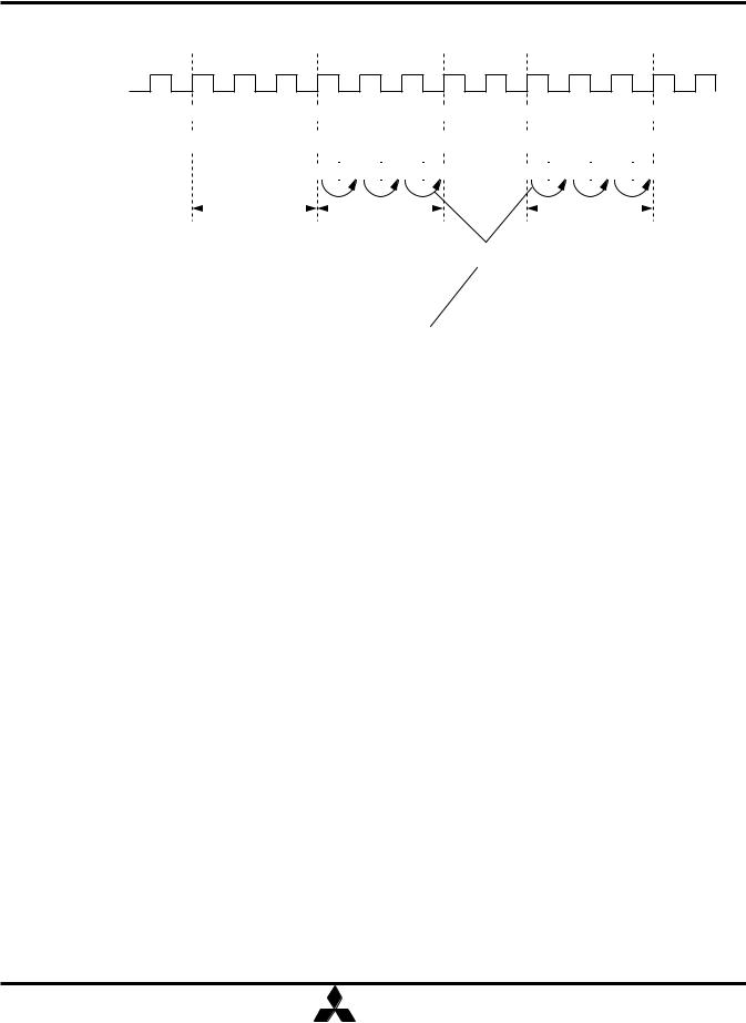
Preliminary Spec. |
MITSUBISHI LSIs |
Some contents are subject to change without notice.
MH4S64BBKG -7,-7L,-8,-8L,-10,-10L
268435456-BIT (4194304 - WORD BY 64-BIT)SynchronousDRAM
CK
Command |
|
Read |
|
|
|
|
|
|
|
|
|
Write |
|
|
|
|
|
||
|
|
|
|
|
|
|
|
|
|
|
|
|
|
|
|
|
|
|
|
Address |
|
Y |
|
|
|
|
|
|
|
|
|
Y |
|
|
|
|
|
||
DQ |
|
|
|
|
|
|
|
|
|
|
|
|
|
|
|
|
|
|
|
|
|
|
|
|
Q0 |
Q1 |
Q2 |
|
Q3 |
|
D0 |
D1 |
D2 |
|
D3 |
|
|||
CL= 3 |
|
|
|
|
|
|
|||||||||||||
|
|
|
|
|
|
|
|
|
|
|
|
|
|
|
|
|
|
|
|
|
|
/CAS Latency |
|
|
Burst Length |
|
|
|
|
|
Burst Length |
|
|
|
|||||
|
BL= 4 |
|
|
|
|
|
|
|
|
|
|
|
|||||||
|
|
|
|
|
|
|
|
|
|
|
|
|
|
|
|
|
|
|
|
|
|
|
|
|
|
|
|
|
|
|
Burst Type |
|
|
|
|
|
|||
Initial Address |
BL |
|
|
|
|
|
|
|
Column Addressing |
|
|
|
|
|
|
|
|
|||||
|
|
|
|
|
|
|
|
|
|
|
|
|
|
|
|
|
|
|
|
|
|
|
A2 |
A1 |
A0 |
|
|
|
|
Sequential |
|
|
|
|
|
|
Interleaved |
|
|
|
|||||
|
|
|
|
|
|
|
|
|
|
|
|
|
|
|
|
|
|
|
|
|
|
|
0 |
0 |
0 |
|
0 |
1 |
2 |
3 |
4 |
|
5 |
6 |
7 |
0 |
1 |
2 |
|
3 |
4 |
|
5 |
6 |
7 |
|
|
|
|
|
|
|
|
|
|
|
|
|
|
|
|
|
|
|
|
|
|
|
0 |
0 |
1 |
|
1 |
2 |
3 |
4 |
5 |
|
6 |
7 |
0 |
1 |
0 |
3 |
|
2 |
5 |
|
4 |
7 |
6 |
|
|
|
|
|
|
|
|
|
|
|
|
|
|
|
|
|
|
|
|
|
|
|
0 |
1 |
0 |
|
2 |
3 |
4 |
5 |
6 |
|
7 |
0 |
1 |
2 |
3 |
0 |
|
1 |
6 |
|
7 |
4 |
5 |
|
|
|
|
|
|
|
|
|
|
|
|
|
|
|
|
|
|
|
|
|
|
|
0 |
1 |
1 |
8 |
3 |
4 |
5 |
6 |
7 |
|
0 |
1 |
2 |
3 |
2 |
1 |
|
0 |
7 |
|
6 |
5 |
4 |
|
|
|
|
|
|
|
|
|
|
|
|
|
|
|
|
|
|
|
|
|
|
|
1 |
0 |
0 |
4 |
5 |
6 |
7 |
0 |
|
1 |
2 |
3 |
4 |
5 |
6 |
|
7 |
0 |
|
1 |
2 |
3 |
|
|
|
|
|
|||||||||||||||||||
|
|
|
|
|
|
|
|
|
|
|
|
|
|
|
|
|
|
|
|
|
|
|
1 |
0 |
1 |
|
5 |
6 |
7 |
0 |
1 |
|
2 |
3 |
4 |
5 |
4 |
7 |
|
6 |
1 |
|
0 |
3 |
2 |
|
|
|
|
|
|
|
|
|
|
|
|
|
|
|
|
|
|
|
|
|
|
|
1 |
1 |
0 |
|
6 |
7 |
0 |
1 |
2 |
|
3 |
4 |
5 |
6 |
7 |
4 |
|
5 |
2 |
|
3 |
0 |
1 |
|
|
|
|
|
|
|
|
|
|
|
|
|
|
|
|
|
|
|
|
|
|
|
1 |
1 |
1 |
|
7 |
0 |
1 |
2 |
3 |
|
4 |
5 |
6 |
7 |
6 |
5 |
|
4 |
3 |
|
2 |
1 |
0 |
|
|
|
|
|
|
|
|
|
|
|
|
|
|
|
|
|
|
|
|
|
|
|
- |
0 |
0 |
|
0 |
1 |
2 |
3 |
|
|
|
|
|
0 |
1 |
2 |
|
3 |
|
|
|
|
|
|
|
|
|
|
|
|
|
|
|
|
|
|
|
|
|
|
|
|
|
|
|
|
- |
0 |
1 |
4 |
1 |
2 |
3 |
0 |
|
|
|
|
|
1 |
0 |
3 |
|
2 |
|
|
|
|
|
|
|
|
|
|
|
|
|
|
|
|
|
|
|
|
|
|
|
|
|
|
|
|
- |
1 |
0 |
2 |
3 |
0 |
1 |
|
|
|
|
|
2 |
3 |
0 |
|
1 |
|
|
|
|
|
|
|
|
|
|
|
|
|
|
|
|
|
|
|||||||||||
|
|
|
|
|
|
|
|
|
|
|
|
|
|
|
|
|
|
|
|
|
|
|
- |
1 |
1 |
|
3 |
0 |
1 |
2 |
|
|
|
|
|
3 |
2 |
1 |
|
0 |
|
|
|
|
|
|
|
|
|
|
|
|
|
|
|
|
|
|
|
|
|
|
|
|
|
|
|
|
- |
- |
0 |
2 |
0 |
1 |
|
|
|
|
|
|
|
0 |
1 |
|
|
|
|
|
|
|
|
|
|
|
|
|
|
|
|
|
|
|
|
|
|
|
|
|
|
|
|
|
|
|
- |
- |
1 |
1 |
0 |
|
|
|
|
|
|
|
1 |
0 |
|
|
|
|
|
|
|
|
|
|
|
|
|
|
|
|
|
|
|
|
|
|
|
|
|
|||||||
|
|
|
|
|
|
|
|
|
|
|
|
|
|
|
|
|
|
|
|
|
|
|
MIT-DS-0295-0.0
MITSUBISHI |
22.Dec.1998 |
ELECTRIC
( 17 / 55 )
 Loading...