


White Electronic Designs EDI88128LP70NC, EDI88128LP70NB, EDI88128LP70CM, EDI88128LP70CI, EDI88128LP70CC Datasheet
...
νAccess Times of 70, 85, 100ns
νAvailable with Single Chip Selects (EDI88128) or Dual Chip Selects (EDI88130)
ν2V Data Retention (LP Versions)
νCS and OE Functions for Bus Control
νTTL Compatible Inputs and Outputs
νFully Static, No Clocks
νOrganized as 128Kx8
νIndustrial, Military and Commercial Temperature Ranges
νThru-hole and Surface Mount Packages JEDEC Pinout
•32 pin Ceramic DIP, 0.6 mils wide (Package 9)
•32 lead Ceramic SOJ (Package 140)
νSingle +5V (±10%) Supply Operation
The EDI88128C is a high speed, high performance, Monolithic CMOS Static RAM organized as 128Kx8.
The device is also available as EDI88130C with an additional chip select line (CS2) which will automatically power down the device when proper logic levels are applied.
The second chip select line (CS2) can be used to provide system memory security during power down in non-battery backed up systems and simplifiy decoding schemes in memory banking where large multiple pages of memory are required.
The EDI88128C and the EDI88130C have eight bi-directional input-output lines to provide simultaneous access to all bits in a word. An automatic power down feature permits the on-chip circuitry to enter a very low standby mode and be brought back into operation at a speed equal to the address access time.
Low power versions, EDI88128LP and EDI88130LP, offer a 2V data retention function for battery back-up opperation. Military product is available compliant to Appendix A of MIL-PRF-38535.
FIG. 1 |
|
|
||||
|
|
32 DIP |
|
I/O0-7 |
DataInputs/Outputs |
|
|
|
32 SOJ |
|
A0-16 |
Address Inputs |
|
|
|
|
|
WE |
Write Enable |
|
|
|
|
CS1, CS2 |
Chip Selects |
||
|
|
|
|
|||
NC |
1 |
32 |
VCC |
OE |
Output Enable |
|
A16 |
2 |
31 |
A15 |
|||
|
|
|||||
A14 |
3 |
30 |
NC/CS2* |
VCC |
Power (+5V ±10%) |
|
A12 |
4 |
29 |
WE |
VSS |
Ground |
|
A7 |
5 |
28 |
A13 |
|||
A6 |
6 |
27 |
A8 |
NC |
Not Connected |
|
A5 |
7 |
26 |
A9 |
|||
A4 |
8 |
25 |
A11 |
|
|
|
A3 |
9 |
24 |
OE |
|
|
|
A2 |
10 |
23 |
A10 |
|
|
|
A1 |
11 |
22 |
CS1 |
|
||
AØ |
12 |
21 |
I/O7 |
|
|
|
I/OØ |
13 |
20 |
I/O6 |
|
|
|
I/O1 |
14 |
19 |
I/O5 |
|
|
|
I/O2 |
15 |
18 |
I/O4 |
|
|
|
VSS |
16 |
17 |
I/O3 |
|
|
|
* Pin 30 is NC for 88128 or CS2 for 88130.
March 2002 Rev. 16 |
|
White Electronic Designs Corporation • (602) 437-1520 • www.whiteedc.com |

|
|
|
|
|
|
|
||
|
|
|
|
|
|
|
||
|
Voltage on any pin relative to Vss |
|
|
|
-0.5 to 7.0 |
V |
||
|
|
|
|
|
|
|
||
|
|
! |
|
|
|
|
||
|
Commercial |
|
|
|
|
|
0 to +70 |
°C |
|
|
|
|
|
|
|
||
|
Industrial |
|
|
|
-40 to +85 |
°C |
||
|
Military |
|
|
|
-55 to +125 |
°C |
||
|
Storage Temperature, Plastic |
|
|
|
-65 to +150 |
°C |
||
|
Power Dissipation |
|
1 |
W |
||||
|
OutputCurrent |
|
20 |
mA |
||||
|
Junction Temperature, TJ |
|
175 |
°C |
||||
NOTE:
Stress greater than those listed under "Absolute Maximum Ratings" may cause permanent damage to the device. This is a stress rating only and functional operation of the device at these or any other conditions greater than those indicated in the operational sections of this specification is not implied. Exposure to absolute maximum rating conditions for extended periods may affect reliability.
|
# $% |
$'$ |
& |
|
AddressLines |
CI |
VIN = Vcc or Vss, f = 1.0MHz |
12 |
pF |
|
|
|
|
|
Input/OutputLines |
CO |
VOUT = Vcc or Vss, f = 1.0MHz |
14 |
pF |
|
|
|
|
|
These parameters are sampled, not 100% tested.
(
|
|
|
|
|
|
|
|
|
|
|
|
|
|
|
|
|
|
|
|
|
|
|
|
|
|
|
|
|
|
|
|
|
$' |
|
|
|
$) |
||||||||||
|
X |
|
H |
|
|
X |
|
X |
|
|
Standby |
High Z |
|
|
Icc2, Icc3 |
||||||||
|
X |
|
X |
|
|
L |
|
X |
|
|
Standby |
High Z |
|
|
Icc2, Icc3 |
||||||||
|
X |
|
X |
|
|
L |
|
X |
|
Output Deselect |
High Z |
|
|
Icc1 |
|||||||||
|
H |
|
L |
|
|
H |
|
H |
|
Output Deselect |
High Z |
|
|
Icc1 |
|||||||||
|
L |
|
L |
|
|
H |
|
H |
|
|
|
Read |
Data Out |
|
Icc1 |
||||||||
|
X |
|
L |
|
|
H |
|
L |
|
|
|
Write |
Data In |
|
|
Icc1 |
|||||||
|
|
|
|
|
|
" " " |
|
|
|
||||||||||||||
|
|
|
|
|
|
|
|
|
|
|
|
|
|
|
|
|
|
|
|
|
|
|
|
|
|
|
|
|
|
# |
$% |
|
|
|
# |
|
|
& |
|
||||||||
Supply Voltage |
|
VCC |
|
4.5 |
|
5.0 |
|
|
5.5 |
V |
|||||||||||||
Supply Voltage |
|
VSS |
|
0 |
|
0 |
|
|
0 |
V |
|||||||||||||
Input High Voltage |
|
VIH |
|
2.2 |
|
— |
|
Vcc +0.5 |
V |
||||||||||||||
Input Low Voltage |
|
VIL |
|
-0.3 |
|
— |
|
|
+0.8 |
V |
|||||||||||||
(
|
# $% |
|
|
|
|
|
|
|
|
|
|
|
|
$'$* |
|
|
|
|
* |
|||||
|
|
|
|
|
|
|
|
|
|
|
|
|
|
|
|
|
|
|
|
|
|
# |
& |
|
Input Leakage Current |
ILI |
VIN = 0V to VCC |
|
-5 |
— |
+5 |
µA |
|||||||||||||||||
Output Leakage Current |
ILO |
VI/O = 0V to VCC, |
|
1 ³ VIH and/or |
|
|
|
-10 |
— |
+10 |
µA |
|||||||||||||
CS |
CS2 £ VIL |
|
||||||||||||||||||||||
|
|
|
|
|
|
|
|
|
|
|
1 = VIL, II/O = 0mA, Min Cycle |
(70-85ns) |
— |
|
120 |
mA |
||||||||
Operating Power Supply Current |
ICC1 |
WE, |
CS |
|
||||||||||||||||||||
|
|
|
|
|
|
|
|
|
|
|
|
|
|
|
|
|
|
(100ns) |
— |
|
110 |
mA |
||
|
|
|
CS2 = VIH |
|
||||||||||||||||||||
Standby (TTL) Power Supply Current |
ICC2 |
|
|
|
|
|
1 ³ VIH and/or |
|
|
2 £ VIL, VIN ³ VIH or £ VIL |
|
— |
|
10 |
mA |
|||||||||
|
|
|
CS |
CS |
|
|
||||||||||||||||||
|
|
|
|
|
1 ³ VCC -0.2V and/or |
|
2 £ Vcc +0.2V |
C |
— |
1 |
5 |
mA |
||||||||||||
|
|
CS |
CS |
|||||||||||||||||||||
Full Standby Power Supply Current |
ICC3 |
VIN ³ Vcc -0.2V or VIN £ 0.2V |
LP |
— |
— |
1 |
mA |
|||||||||||||||||
OutputLowVoltage |
VOL |
IOL = 2.1mA |
|
— |
— |
0.4 |
V |
|||||||||||||||||
Output High Voltage |
VOH |
IOH = -1.0mA |
|
2.4 |
— |
— |
V |
|||||||||||||||||
|
|
|
|
|
|
|
|
|
|
|
|
|
|
|
|
|
|
|
|
|
|
|
|
|
NOTE: DC test conditions : VIL = 0.3V, VIH = Vcc -0.3V
White Electronic Designs Corporation • Phoenix AZ • (602) 437-1520 |
|
( " +
|
# $% |
|
|
,-* |
|
./ * |
|
0--* |
|
||||
|
1 " |
% 2 |
|
|
& |
|
|
& |
|
|
& |
* |
|
|
|
|
|
|
|
|
|
|
|
|
|
|
|
Read Cycle Time |
tAVAV |
|
tRC |
70 |
|
|
85 |
|
|
100 |
|
|
ns |
AddressAccessTime |
tAVQV |
|
tAA |
|
|
70 |
|
|
85 |
|
|
100 |
ns |
|
|
|
|
|
|
|
|
|
|
|
|
|
|
ChipSelectAccessTime |
tELQV |
|
tACS |
|
|
70 |
|
|
85 |
|
|
100 |
ns |
|
tSHQV |
|
tACS |
|
|
70 |
|
|
85 |
|
|
100 |
ns |
ChipSelecttoOutput inLowZ (1) |
tELQX |
|
tCLZ |
3 |
|
|
3 |
|
|
3 |
|
|
ns |
|
tSHQX |
|
tCLZ |
3 |
|
|
3 |
|
|
3 |
|
|
ns |
|
|
|
|
|
|
|
|
|
|
|
|
|
|
ChipDisabletoOutputinHighZ (1) |
tEHQZ |
|
tCHZ |
0 |
|
30 |
0 |
|
30 |
0 |
|
30 |
ns |
|
tSLQZ |
|
tCHZ |
0 |
|
30 |
0 |
|
30 |
0 |
|
30 |
ns |
|
|
|
|
|
|
|
|
|
|
|
|
|
|
OutputHoldfromAddressChange |
tAVQX |
|
tOH |
3 |
|
|
3 |
|
|
3 |
|
|
ns |
OutputEnabletoOutputValid |
tGLQV |
|
tOE |
|
|
25 |
|
|
30 |
|
|
50 |
ns |
|
|
|
|
|
|
|
|
|
|
|
|
|
|
OutputEnabletoOutputinLowZ(1) |
tGLQX |
|
tOLZ |
0 |
|
|
0 |
|
|
0 |
|
|
ns |
|
|
|
|
|
|
|
|
|
|
|
|
|
|
OutputDisabletoOutputinHighZ(1) |
tGHQZ |
|
tOHZ |
0 |
|
30 |
0 |
|
30 |
0 |
|
30 |
ns |
|
|
|
|
|
|
|
|
|
|
|
|
|
|
1. This parameter is guaranteed by design but not tested.
" |
|
|
|
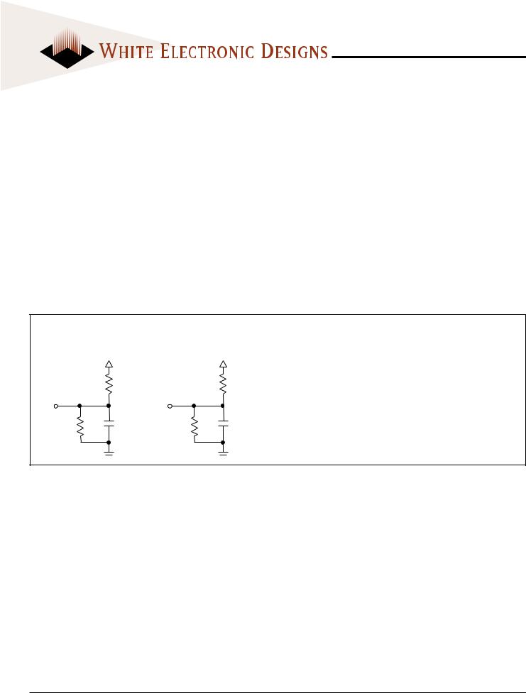
Figure 1 |
Vcc |
Figure 2 |
Vcc |
|
|
||
|
480Ω |
|
480Ω |
Q |
|
Q |
|
255Ω |
30pF |
255Ω |
5pF |
Input Pulse Levels |
VSS to 3.0V |
|
|
Input Rise and Fall Times |
5ns |
|
|
Input and Output Timing Levels |
1.5V |
|
|
OutputLoad |
Figure 1 |
|
|
NOTE: For tEHQZ, tGHQZ and tWLQZ, CL = 5pF Figure 2)
White Electronic Designs Corporation • (602) 437-1520 • www.whiteedc.com
 Loading...