


KLV-40W300A
Table of contents
 Loading...
LCD COLOR TELEVISION
SERVICE MANUAL
FIX2
CHASSIS
MODEL NAME REMOTE COMMANDER DESTINATION
9-883-767-01
KLV-40W300A
RM-YD017 BRAZIL
KLV-46W300A
RM-YD017 BRAZIL
KLV-52W300A
RM-YD017 BRAZIL
HISTORY INFORMATION FOR THE FOLLOWING MANUAL:
ORIGINAL MANUAL ISSUE DATE: 10/2007
REVISION DATE SUBJECT
10/2007 No revisions or updates are applicable at this time.

LCD COLOR TELEVISION
SERVICE MANUAL
FIX2
CHASSIS
MODEL NAME REMOTE COMMANDER DESTINATION
9-883-767-01
KLV-40W300A
RM-YD017 BRAZIL
KLV-46W300A
RM-YD017 BRAZIL
KLV-52W300A
RM-YD017 BRAZIL
Self Diagnosis
Supported model
KLV-46W300A RM-YD017

3
KLV-40W300A/46W300A/52W300A
KLV-40W300A/46W300A/52W300A
TABLE OF CONTENTS
SECTION TITLE PAGE SECTION TITLE PAGE
Specifi cations ................................................................................. 4
Warnings and Cautions .................................................................. 6
Safety-Related Component Warning .............................................. 7
Safety Check-Out ........................................................................... 9
Self-Diagnostic Function ............................................................... 10
SECTION 1: DISASSEMBLY ............................................................... 12
1-1. Rear Cover Removal ............................................................ 12
1-2. Arm and Stand Removal ...................................................... 12
1-3. Speakers, HW3 Board, and AC Inlet Removal ..................... 13
1-4. HW1 Board Removal ........................................................... 13
1-5. HW2 Board Removal ........................................................... 14
1-6 AU Board and FB1 Board Removal ..................................... 14
1-7. TUU2 Board Removal .......................................................... 15
1-8. DF1, DF2, DF3 Boards and GF1 Board Removal
(KLV-40W300A/46W300A Only) ....................................... 16
1-9. DF4, DF5 Boards and GF2 Board Removal
(KLV-52W300A Only) ........................................................ 17
1-10. Stay (Bracket) Removal ....................................................... 18
1-11. LCD Panel Removal ............................................................. 18
SECTION 2: SERVICE ADJUSTMENTS ............................................. 19
2-1. Remote Adjustment Buttons and Indicators ......................... 19
2-2. Accessing Service Adjustments ........................................... 19
2-3. Updating Model Information after
Replacing the FB1 Board ..................................................... 21
SECTION 3: DIAGRAMS ..................................................................... 22
3-1. Circuit Boards Location ........................................................ 22
3-2. Printed Wiring Boards and
Schematic Diagrams Information ......................................... 22
3-3. Block Diagram ...................................................................... 24
3-3-1. Connector Diagram (KLV-40W300A Only) ............... 25
3-3-2. Connector Diagram (KLV-46W300A Only) ............... 26
3-3-3. Connector Diagram (KLV-52W300A Only) ............... 27
3-4. Schematics and Supporting Information .............................. 28
AU Board Schematic Diagram (1 of 6) ................................. 28
AU Board Schematic Diagram (2 of 6) ................................. 29
AU Board Schematic Diagram (3 of 6) ................................. 30
AU Board Schematic Diagram (4 of 6) ................................. 31
AU Board Schematic Diagram (5 of 6) ................................. 32
AU Board Schematic Diagram (6 of 6) ................................. 33
DF1 Board Schematic Diagram (KLV-40W300A Only) ........ 35
DF2 Board Schematic Diagram (KLV-46W300A Only) ........ 38
DF3 Board Schematic Diagram (KLV-46W300A Only) ........ 41
DF4 Board Schematic Diagram (KLV-52W300A Only) ........ 44
DF5 Board Schematic Diagram (KLV-52W300A Only) ........ 46
FB1 Board Schematic Diagram (1 of 16) ............................. 48
FB1 Board Schematic Diagram (2 of 16) ............................. 49
FB1 Board Schematic Diagram (3 of 16) ............................. 50
FB1 Board Schematic Diagram (4 of 16) ............................. 51
FB1 Board Schematic Diagram (5 of 16) ............................. 52
FB1 Board Schematic Diagram (6 of 16) ............................. 53
FB1 Board Schematic Diagram (7 of 16) ............................. 54
FB1 Board Schematic Diagram (8 of 16) ............................. 55
FB1 Board Schematic Diagram (9 of 16) ............................. 56
FB1 Board Schematic Diagram (10 of 16) ........................... 57
FB1 Board Schematic Diagram (11 of 16) ........................... 58
FB1 Board Schematic Diagram (12 of 16) ........................... 59
FB1 Board Schematic Diagram (13 of 16) ........................... 60
FB1 Board Schematic Diagram (14 of 16) ........................... 61
FB1 Board Schematic Diagram (15 of 16) ........................... 62
FB1 Board Schematic Diagram (16 of 16) ........................... 63
GF1 Board Schematic Diagram
(KLV-40W300A/46W300A Only) ...................................... 65
GF2 Board Schematic Diagram (KLV-52W300A Only) ........ 68
HW1 Board Schematic Diagram .......................................... 71
HW2 Board Schematic Diagram (1 of 2) .............................. 73
HW2 Board Schematic Diagram (2 of 2) .............................. 74
HW3 Board Schematic Diagram .......................................... 77
TUU2 Board Schematic Diagram (1 of 2) ............................ 79
TUU2 Board Schematic Diagram (2 of 2) ............................ 80
3-5. Semiconductors ................................................................... 83
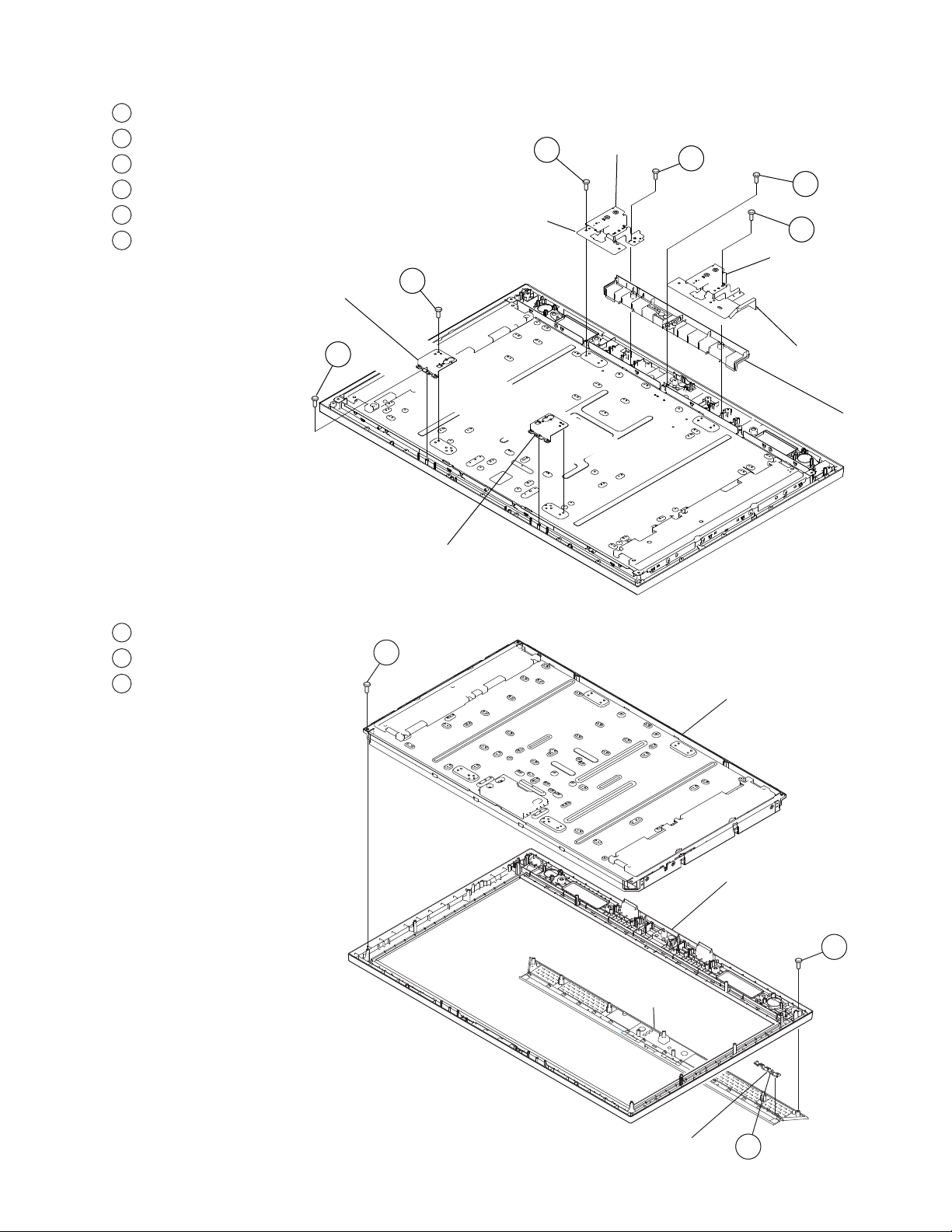
SECTION 4: EXPLODED VIEWS ........................................................ 84
4-1. Rear Cover Assembly and Stand Assembly ........................ 84
4-2. Chassis ................................................................................ 85
4-3. Connectors ........................................................................... 86
4-4. Speakers .............................................................................. 87
4-5. Bezel Assembly and LCD Panel .......................................... 88
SECTION 5: ELECTRICAL PARTS LIST ............................................ 89
APPENDIX A: ENCRYPTION KEY COMPONENTS ..........................A-1

4
KLV-40W300A/46W300A/52W300A
KLV-40W300A/46W300A/52W300A
SPECIFICATIONS
Design and specifi cations are subject to change without notice.
120V-240V AC, 50/60Hz
220W (KLV-40W300A Only)
260W (KLV-46W300A Only)
295W (KLV-52W300A Only)
Less than 0.4W
VIDEO (IN) 1/2/3:
S Video (4-Pin Mini DIN (VIDEO 1 Only)
Y: 1.0 Vp-p, 75 ohms unbalanced, sync negative
C: 0.286 Vp-p (Burst signal), 75 ohms
Video
1.0 Vp-p, 75ohms unbalanced, sync negative
Audio
500 mVrms (100% modulation)
Impedance:47 kilohms
COMPONENT IN 1/2:
YP
B
P
R
(Component Video)
Y:1.0 Vp-p, 75 ohms unbalanced, sync negative
P
B
:0.7 Vp-p, 75 ohms
P
R
:0.7 Vp-p, 75 ohms
Signal format: 480i, 480p, 720p, 1080i, 1080p
AUDIO
500 mVrms (100% modulation)
Impedance: 47 kilohms
HDMI IN 1/2/3:
Power Requirements
Power Consumption (W)
In Use (Max)
In Standby
HDMI: Video:480i, 480p, 720p, 1080i,1080p, 1080/24p
Audio: Two channel linear PCM 32, 44.1 and
48 kHz, 16, 20 and 24 bits, Dolby Digital
AUDIO (for HDMI IN 1):
500 mVrms (100% modulation)
Impedance: 47 kilohms
AUDIO OUT:
500 mVrms (100% modulation) (Fixed)
1 Vrms at the maximum volume setting (Variable)
PC IN:
D-sub 15-pin, analog RGB, 0.7 Vp-p, 75 ohms, positive
PC AUDIO INPUT:
Stereo mini jack, 500 mVrms (100% modulation)
Impedance: 47 kilohms
HEADPHONES:
Stereo mini jack
Impedance: 16 ohms
Trademark Information
As an ENERGY STAR
®
Partner, Sony
Corporation has determined that this product
meets the ENERGY STAR
®
guidelines for
energy efficiency.
ENERGY STAR
®
is a U.S. registered mark.
This TV incorporates High-
Definition Multimedia Interface
(HDMI
™
) technology. HDMI, the HDMI logo and High-
Definition Multimedia Interface are trademarks or
registered trademarks of HDMI Licensing LLC.
This TV is manufactured under license from Dolby
Laboratories. “Dolby” and the double-D symbol are
trademarks of Dolby Laboratories.
Blu-ray Disc is a trademark.
“BRAVIA” and , BRAVIA ENGINE EX, “XMB”
and “XrossMediaBar”, S-Force, BRAVIA Theatre Sync, , DM
x
,
BRAVIA Internet Video Link Ready and “PS3” are trademarks
or registered marks of Sony Corporation and/or
Son
y
Computer Entertainment Inc.

5
KLV-40W300A/46W300A/52W300A
KLV-40W300A/46W300A/52W300A
Television system
NTSC 3.58/PAL-M/PAL-N
Trinorma
Channel coverage
VHF: 2-13
UHF: 14-69
CATV: 1-125
Antenna
75-ohm external terminal for VHF/UHF
Panel System
LCD (Liquid Crystal Display) Panel
Display Resolution (horizontal x vertical):
1,920 dots x 1,080 lines
Screen Size (measured diagonally)
KLV-40W300A - ~40 inches/101.6 cm
KLV-46W300A - ~46 inches/116.8 cm
KLV-52W300A - ~52 inches/132.1 cm
Supplied Accessories
Remote Commander RM-YD017
Two Size AA (R6) Batteries
AC Power Cord
Suport Belt (Lock Assy, Rudder) Securing Screw,
and Wood Screw
(See Bag Assy, Rudder Lock in the Accessories and Packing
section of the Electrical Parts List in this manual.)
Cable Holder (1 attached to the TV)
Operating Instructions
Quick Setup Guide
Optional Accessories
Headphones Plug Adaptor
Connecting Cables
KLV-40W300A KLV-46W300A KLV-52W300A
Speakers
Output
Dimensions (W x H)
1
5/8
x 5
7/8
inches 2
1/8
x 6
1/8
inches 2
6/8
x 5
1/8
inches
42 x 150 mm 55 x 155 mm 70 x 130 mm
Tweete
r
Dimensions (H)
1
5/8
inches 1
5/8
inches 1
5/8
inches
40 mm 40 mm 40 mm
Dimensions (W x H x D)
with stand
39
1/8
x 27
1/8
x 10
1/2
inches 44
3/4
x 30
3/4
x 12
1/8
inches 50
3/8
x 34
1/2
x 15
1/8
inches
992 x 688 x 265 mm 1135 x 799 x 306 mm 1278 x 874 x 384 mm
without stand
39
1/8
x 25
3/8
x 4
7/8
inches 44
3/4
x 29 x 4
7/8
inches 50
3/8
x 32
7/8
x 4
7/8
inches
992 x 643 x 122 mm 1135 x 735 x 122 mm 1278 x 832 x 123 mm
wall-mount hole pattern 300 x 200 mm 300 x 200 mm 400 x 300 mm
Mass
with stand 56 lbs. 71 lbs. 95 lbs.
25.0 kg 32.0 kg 43.0 kg
without stand 48 lbs. 62 lbs. 79 lbs.
21.5 kg 28.0 kg 35.5 kg
11W+11W
All measurements are approximations.
6
KLV-40W300A/46W300A/52W300A
KLV-40W300A/46W300A/52W300A
WARNINGS AND CAUTIONS
CAUTION
These servicing instructions are for use by qualifi ed service personnel only. To reduce the risk of electric shock, do not perform any servicing other
than that contained in the operating instructions unless you are qualifi ed to do so.
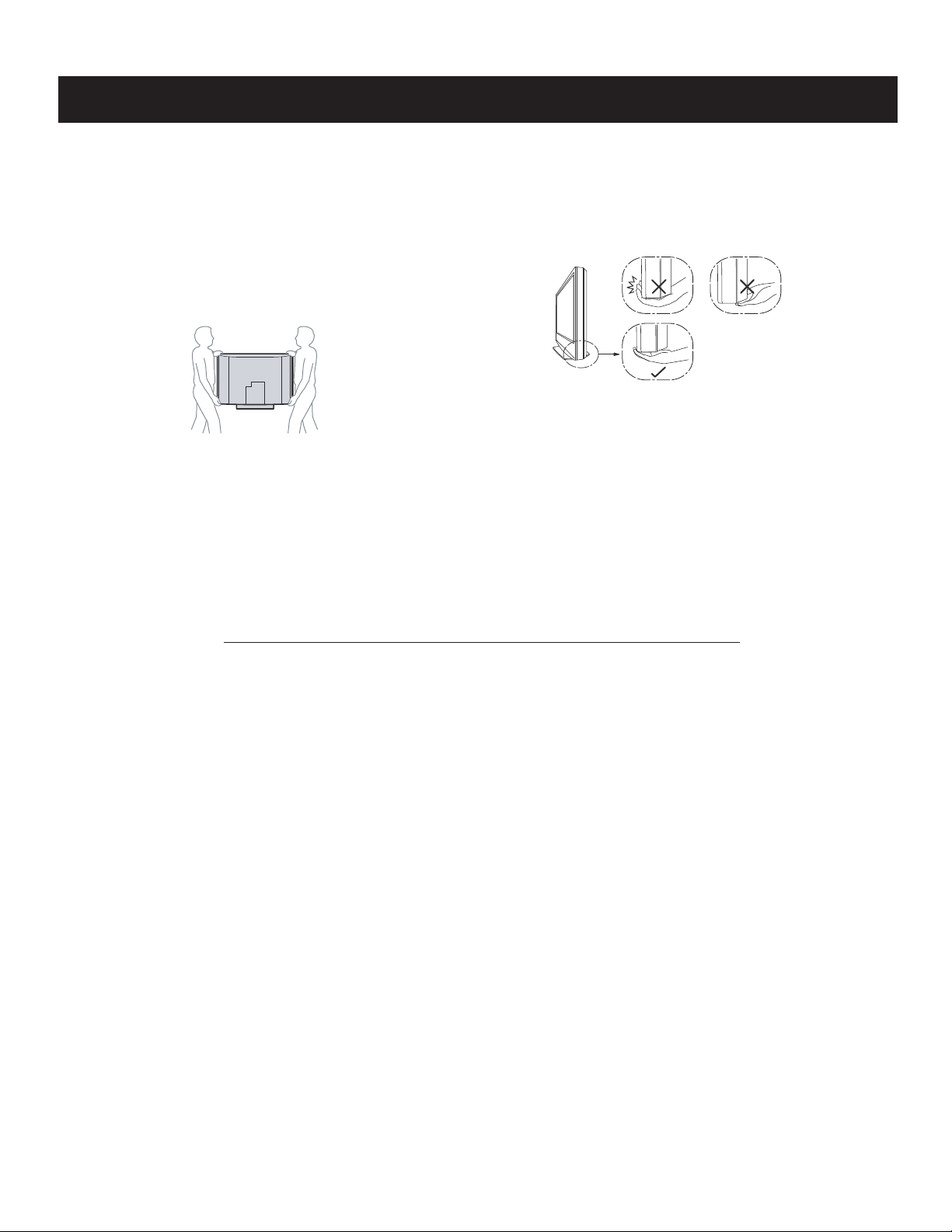
CARRYING THE TV
To avoid dropping the TV and causing serious injury, be sure to follow
these guidelines:
s Before carrying the TV, disconnect all cables.
s Carrying the large size TV requires two or more people.
s When you carry the TV, place your hand as illustrated and hold it
securely. Do not put stress on the LCD panel.
s When lifting or moving the TV, hold it firmly from the bottom. Place
your palm directly under the panel.
s When carrying, do not subject the TV to shocks or vibration, or
excessive force.
WARNING!!
An isolation transformer should be used during any service to avoid possible shock hazard, because of live chassis. The chassis of this receiver is
directly connected to the ac power line.
! SAFETY-RELATED COMPONENT WARNING!!
Components identifi ed by shading and
!
mark on the schematic diagrams, exploded views, and in the parts list are critical for safe operation. Replace
these components with Sony parts whose part numbers appear as shown in this manual or in supplements published by Sony. Circuit adjustments that
are critical for safe operation are identifi ed in this manual. Follow these procedures whenever critical components are replaced or improper operation is
suspected.

7
KLV-40W300A/46W300A/52W300A
KLV-40W300A/46W300A/52W300A
SAFETY-RELATED COMPONENT WARNING
There are critical components used in LCD color TVs that are important for safety. These components are identifi ed with shading and
!
mark on the schematic diagrams and the electrical parts list. It is essential that these critical parts be replaced only with the part number
specifi ed in the electrical parts list to prevent electric shock, fi re, or other hazard.
NOTE: Do not modify the original design without obtaining written permission from the manufacturer or you will void the original parts and
labor guarantee.
USE CAUTION WHEN HANDLING THE LCD PANEL
When repairing the LCD panel, be sure you are grounded by using a wrist band.
When installing the LCD panel on a wall, the LCD panel must be secured using the 4 mounting holes on the rear cover.
To avoid damaging the LCD panel:
do not press on the panel or frame edge to avoid the risk of electric shock.
do not scratch or press on the panel with any sharp objects.
do not leave the module in high temperatures or in areas of high humidity for an extended period of time.
do not expose the LCD panel to direct sunlight.
avoid contact with water. It may cause a short circuit within the module.
disconnect the AC adapter when replacing the backlight (CCFL) or inverter circuit.
(High voltage occurs at the inverter circuit at 650Vrms.)
always clean the LCD panel with a soft cloth material.
use care when handling the wires or connectors of the inverter circuit. Damaging the wires may cause a short.
protect the panel from ESD to avoid damaging the electronic circuit (C-MOS).
LEAKAGE CURRENT HOT CHECK CIRCUIT
8
KLV-40W300A/46W300A/52W300A
KLV-40W300A/46W300A/52W300A
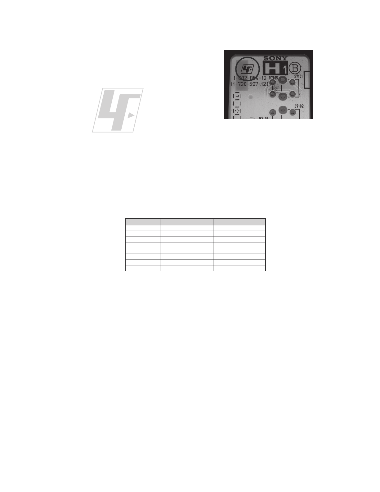
The circuit boards used in these models have been processed using
Lead Free Solder. The boards are identified by the LF logo located
close to the board designation e.g. H1 etc [ see example ]. The
servicing of these boards requires special precautions to be taken as
outlined below.
example 1
It is strongly recommended to use Lead Free Solder material in order to guarantee optimal quality of new solder joints.
Lead Free Solder is available under the following part numbers :
Due to the higher melting point of Lead Free Solder the soldering iron tip temperature needs to be set to 370 degrees centigrade.
This requires soldering equipment capable of accurate temperature control coupled with a good heat recovery characteristics.
For more information on the use of Lead Free Solder, please refer to
http://www.sony-training.com
rebmuntraP retemaiD skrameR
91-500-046-7mm3.0gK52.0
02-500-046-7mm4.0gK05.0
12-500-046-7mm5.0gK05.0
22-500-046-7mm6.0gK52.0
32-500-046-7mm8.0gK00.1
42-500-046-7mm0.1gK00.1
52-500-046-7mm2.1gK00.1
62-500-046-7mm6.1gK00.1
9
KLV-40W300A/46W300A/52W300A
KLV-40W300A/46W300A/52W300A
SAFETY CHECK-OUT
After correcting the original service problem, perform the following
safety checks before releasing the set to the customer:
1. Check the area of your repair for unsoldered or poorly soldered
connections. Check the entire board surface for solder splashes and
bridges.
2. Check the interboard wiring to ensure that no wires are “pinched” or
touching high-wattage resistors.
3. Check that all control knobs, shields, covers, ground straps, and
mounting hardware have been replaced. Be absolutely certain that
you have replaced all the insulators.
4. Look for unauthorized replacement parts, particularly transistors,
that were installed during a previous repair. Point them out to the
customer and recommend their replacement.
5. Look for parts which, though functioning, show obvious signs of
deterioration. Point them out to the customer and recommend their
replacement.
6. Check the line cords for cracks and abrasion. Recommend the
replacement of any such line cord to the customer.
7. Check the antenna terminals, metal trim, “metallized” knobs, screws,
and all other exposed metal parts for AC leakage. Check leakage as
described below.
Leakage Test
The AC leakage from any exposed metal part to earth ground and
from all exposed metal parts to any exposed metal part having a
return to chassis, must not exceed 0.5 mA (500 microamperes).
Leakage current can be measured by any one of three methods.
1. A commercial leakage tester, such as the Simpson 229 or RCA
WT-540A. Follow the manufacturers’ instructions to use these
instructions.
2. A battery-operated AC milliampmeter. The Data Precision 245
digital multimeter is suitable for this job.
3. Measuring the voltage drop across a resistor by means of a VOM
or battery-operated AC voltmeter. The “limit” indication is 0.75
V, so analog meters must have an accurate low voltage scale.
The Simpson’s 250 and Sanwa SH-63TRD are examples of
passive VOMs that are suitable. Nearly all battery-operated digital
multimeters that have a 2 VAC range are suitable (see Figure A).
How to Find a Good Earth Ground
A cold-water pipe is a guaranteed earth ground; the cover-plate
retaining screw on most AC outlet boxes is also at earth ground. If the
retaining screw is to be used as your earth ground, verify that it is at
ground by measuring the resistance between it and a cold-water pipe
with an ohmmeter. The reading should be zero ohms.
If a cold-water pipe is not accessible, connect a 60- to 100-watt
trouble- light (not a neon lamp) between the hot side of the receptacle
and the retaining screw. Try both slots, if necessary, to locate the hot
side on the line; the lamp should light at normal brilliance if the screw
is at ground potential (see Figure B).
To Exposed Metal
Parts on Set
0.15 F
Earth Ground
AC
Voltmeter
(0.75V)
Trouble Light
AC Outlet Box
Ohmmeter
Cold-water Pipe
Figure A. Using an AC voltmeter to check AC leakage. Figure B. Checking for earth ground.
10
KLV-40W300A/46W300A/52W300A
KLV-40W300A/46W300A/52W300A
SELF-DIAGNOSTIC FUNCTION
Self Diagnosis
Supported model
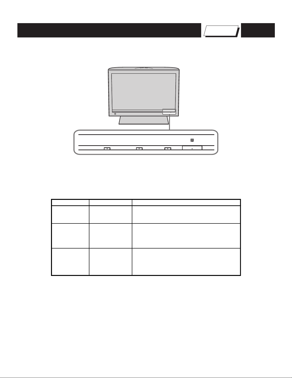
Control Buttons
PIC OFF/TIMER STANDBY POWER
Description of LED Indictors
LED LED Type Description
* Light when the TV set is on
* If LED blinks continuously, this may indicate
that the TV needs servicing.
STANDBY LED
PIC OFF/
TIMER
LED
* Lights up in red when TV is in PC standby mode.
* Lights up in green when Picture Off is activated
* Lights up in orange when the timer is set
When timer is set, the LED remains lit even
when the TV is turned off.
POWER LED
Green or Orange
LED
Green LED
Red LED
11
KLV-40W300A/46W300A/52W300A
KLV-40W300A/46W300A/52W300A
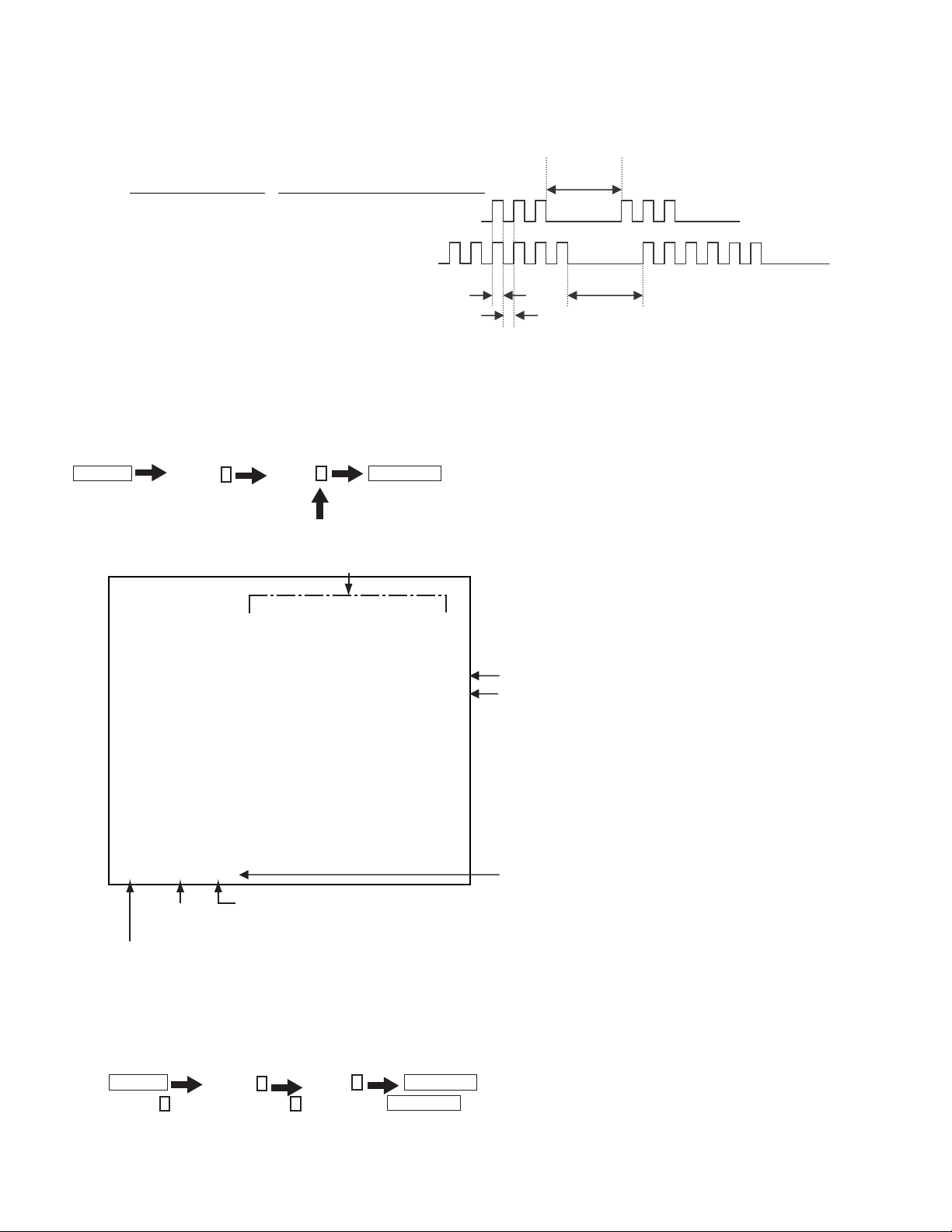
The units in this manual contain a self-diagnostic function. If an error occurs, the STANDBY LED automatically begins to fl ash. The number of times
the LED fl ashes translates to a probable source of the problem. A defi nition of the STANDBY LED fl ash indicators is listed in the instruction manual for
the user’s knowledge and reference. If an error symptom is diffi cult to reproduce use the Remote Commander to display the record that is stored at the
internal NVM to specify the cause.
Number of times LED Flash
POW_ERR1 3 times
BACKLITE 6 times
LED ON : 0.3 sec
LED OFF : 0.3sec
LED OFF
3.0 sec
LED OFF
3.0 sec
Example Diagnosis
- One flash is not used for self-diagnosis.
Diagnostic Indicators
When an error occurs, the STANDBY LED fl ashes a set number of times to indicate the possible cause of the problem. If there is more than one error,
the LED will identify the fi rst of the problem areas. If the errors occur simultaneously, the one that corresponds to the fewest fl ashes is identifi ed fi rst.
(Results for all of the following diagnostic items are displayed on screen. No error has occurred if the screen displays a “00”)
1. TV must be in standby mode. (Power off).
2. Press the following buttons on the Remote Commander within a second of each other:
DISPLAY
Channel
5
Volume
-
TV POWER
.
The Self Check list displays.
This differs from accessing Service Adjustments.
alpsiDDEL
y
stnetnoC
: 000
------------ ------------ ------------ ====
00
====
PVO_WOP: 200
------------ ------------ ------------
PVO rewoP00
1RRE_WOP: 300
------------ ------------ ------------
rorrE rewoP00
NOC_T: 500
------------ ------------ ------------
rorrE NOC-T00
ETILKCAB: 600
------------ ------------ ------------
rorrE thgilkcaBdetceted saw rorre on setacidni 000
PMETLNAP: 700
------------ ------------ ------------
rorrE pmeT lenaPdetceted saw rorre na setacidni 110
TORP_DUA: 800
------------ ------------ ------------
rotcetorP oiduA00
RRE_NAF: 900
------------ ------------ ------------
d
om eseht ni desU toN00
RRE_TTD:010
------------ ------------ ------------
00
:110
------------ ------------ ------------ ====
00
====
RECNALAB:310
------------ ------------ ------------
rorrE lenaP00
TDW_TTD: 101
------------ ------------ ------------
00
miT goD hctaW -TDW
TDW_MVT: 201
------------ ------------ ------------
sremiT goD hctaW(00
TDW_MEB: 301
------------ ------------ ------------
kcart ot desu era 00
,srossecorp orcim
).srorre drocer ot tonemit noitarepo dna tnuoc tooB0000-35000-97200
KCEHC FLES
Operating Hours
(max 65535)
Panel Hours
(max 65535)
Information Indicator displays time of last 3 events
(Not used in FIX2 models)
Boot count
(max 65535)
Resetting the Diagnostic Indicators
After completing the repair of the set, reset the Self Check screen to set all the display results to “00”.
1. TV must be in standby mode. (Power off).
2. Press
DISPLAY
Channel
5
Volume
-
TV POWER
.
3. Press Channel
8
, then press Channel
0
. To exit press
TV POWER
.
12
KLV-40W300A/46W300A/52W300A
KLV-40W300A/46W300A/52W300A
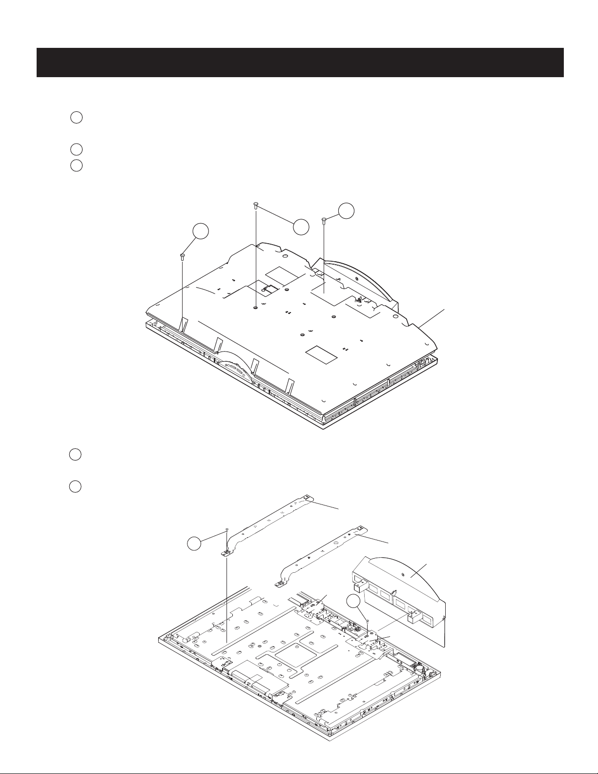
1-1. REAR COVER REMOVAL
SECTION 1: DISASSEMBLY
1
Remove 15 screws from Rear Cover, +BVTP2 4X16 (KLV-40W300A),
Remove 19 screws from Rear Cover, +BVTP2 4X16 (KLV-46W300A/52W300A)
2
Remove 2 screws from Rear Cover arm positions, +PSW M5X12
3
Remove 2 screws from Terminals, +BVTP 3X12 TYPE2 IT-3
1
2
3
Rear Cover
1-2. ARM AND STAND REMOVAL
1
Remove 4 screws from Arms, +PSW M5X8 (KLV-40W300A),
Remove 8 screws from Arms, +PSW M5X8 (KLV-46W300A/52W300A)
2
Remove 4 screws from lower Stays and Stand, +PSW M5X12
1
2
Arm (L)
Arm (R)
Stand Assembly
Stay
Stay
13
KLV-40W300A/46W300A/52W300A
KLV-40W300A/46W300A/52W300A
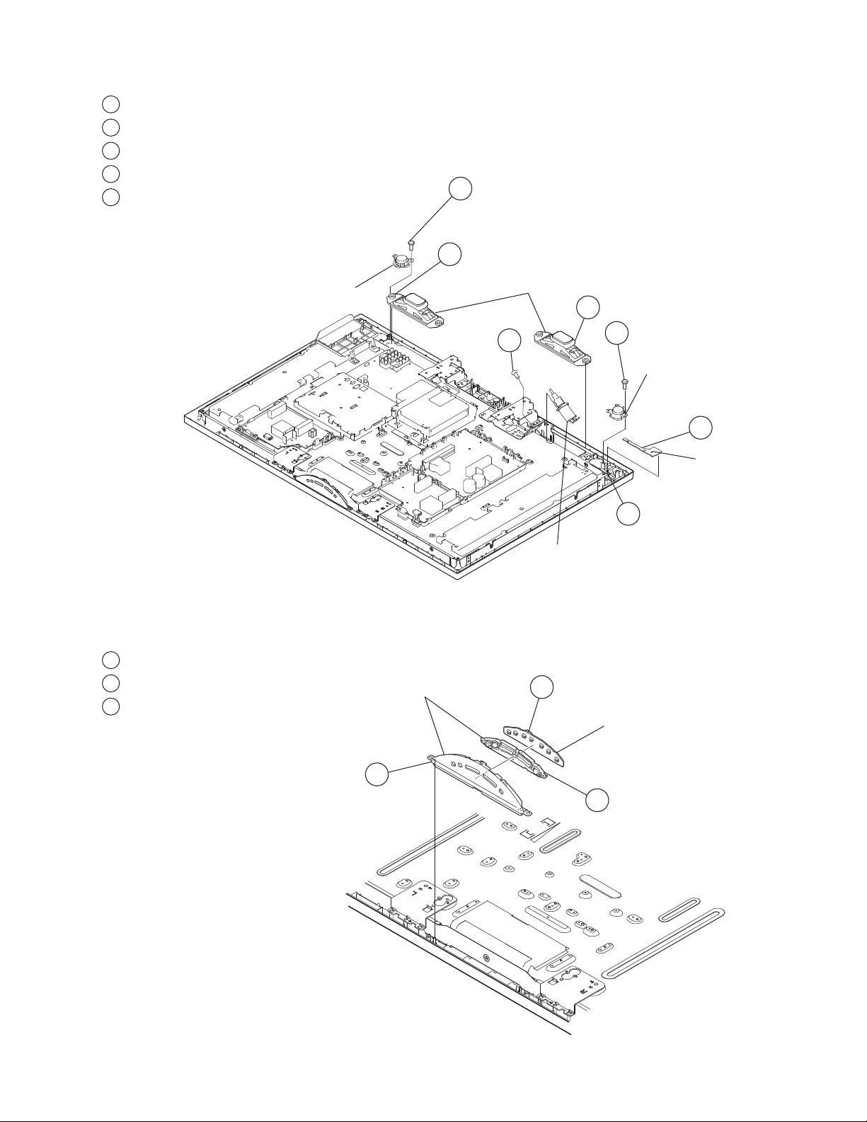
1-3. SPEAKERS, HW3 BOARD, AND AC INLET REMOVAL
1-4. HW1 BOARD REMOVAL
5
1
1
2
2
3
4
Speaker (Tweeter)
Loud Speaker
Speaker (Tweeter)
HW3 Board
AC Inlet
1
Remove 6 screws, +BVTP2 4X16 (KLV-46W300A/52W300A Only)
2
Slide out Loudspeakers from Bezel
3
Remove 2 screws, +KTT 3X10
4
Disconnect 1 connector from HW3 Board
5
Release hook and remove HW3 Board
1
Remove from bezel
2
Disconnect 1 connector
3
Release hooks and remove HW1 Board
1
2
3
Multi Button Assembly
HW1 Board
14
KLV-40W300A/46W300A/52W300A
KLV-40W300A/46W300A/52W300A
1-5. HW2 BOARD REMOVAL
1
Remove 3 screws, +BVTP 3X12 TYPE2 IT-3
2
Disconnect 2 connectors
3
Remove 2 screws, +PVST 3X8 (KLV-40W300A Only)
Remove 2 screws, +PSW M3X5 (KLV-46W300A/52W300A Only)
2
3
1
HW2 Board
Side Terminal Bracket
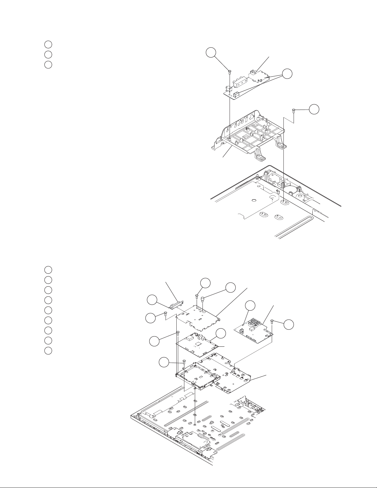
1-6 AU BOARD AND FB1 BOARD REMOVAL
1
Slide out Card Bracket
2
Remove 2 screws, +PSW M3X5
3
Remove 2 screws, HEX
4
Remove 4 screws, +BVST 3X8
5
Remove 7 screws, +BVST 3X8
6
Disconnect 7 connectors
7
Disconnect 7 connectors
8
Remove 9 screws, +BVST 3X8
9
Remove 8 screws, +PSW M3X5
4
1
2
3
7
8
5
6
9
AU Board
Chassis Bracket
FB1 Board
FB Shield (Top)
Card Bracket

15
KLV-40W300A/46W300A/52W300A
KLV-40W300A/46W300A/52W300A
1-7. TUU2 BOARD REMOVAL
2
4
3
5
1
6
Chassis Bracket
TUU Shield (Top)
TUU Shield (Bottom)
TUU2 Board
Tuner Bracket
1
Remove 2 screws, +BVST 3X8
2
Remove 1 Hex Nut from Tuner
3
Remove Tuner Bracket
4
Disconnect 1 connector
5
Remove 5 screws, +BVST 3X8
6
Remove 4 screws, +BVST 3X8

16
KLV-40W300A/46W300A/52W300A
KLV-40W300A/46W300A/52W300A
1
2
4
3
6
5
G/D Bracket
GF1 Board
DF3 Bracket
(KLV-46W300A)
DF3 Board(KLV-46W300A)
DF1 Board(KLV-40W300A)
DF2 Board(KLV-46W300A)
1-8. DF1, DF2, DF3 BOARDS AND GF1 BOARD REMOVAL
(KLV-40W300A/46W300A ONLY)
1
Remove 5 screws, +PSW 3SG (KLV-46W300A Only)
2
Disconnect 3 connectors (KLV-46W300A Only)
3
Disconnect 4 connectors (KLV-40W300A Only)
Disconnect 4 connectors (KLV-46W300A Only)
4
Remove 4 screws, +PSW 3SG
5
Disconnect 7 connectors
6
Remove 4 screws, +PSW 3SG

17
KLV-40W300A/46W300A/52W300A
KLV-40W300A/46W300A/52W300A
1
2
4
3
6
5
G/D Bracket
GF2 Board
DF4 Board
DF5 Bracket
DF5 Board
1
Remove 5 screws, +PSW 3SG
2
Disconnect 3 connectors
3
Disconnect 4 connectors
4
Remove 4 screws, +PSW 3SG
5
Disconnect 7 connectors
6
Remove 4 screws, +PSW 3SG
1-9. DF4, DF5 BOARDS AND GF2 BOARD REMOVAL
(KLV-52W300A ONLY)
18
KLV-40W300A/46W300A/52W300A
KLV-40W300A/46W300A/52W300A
1-10. STAY (BRACKET) REMOVAL
4
3
2
1
Upper Stay (Left)
Stand Holder
Stand Holder
Lower Stay (Left)
Upper Stay (Right)
Lower Stay (Right)
Under Cover
6
5
1
2
3
LED Guide
LCD Panel
Bezel
Speaker Cover
1
Remove 2 screws, +PSW M5X8
2
Remove 2 screws, +BVTP2 4X16
3
Remove 4 screws, +PSW M5X8
4
Remove 4 screws, +BVTP2 4X16
5
Remove 4 screws, +BVTP 4X8
6
Remove 3 screws, +BVTP2 4X16 (KLV-52W300A Only)
1
Remove 4 screws, +BVTP2 4X16
2
Remove 4 screws, +BVTP2 4X16
3
Pop off from Speaker Cover
1-11. LCD PANEL REMOVAL

19
KLV-40W300A/46W300A/52W300A
KLV-40W300A/46W300A/52W300A
2-1. REMOTE ADJUSTMENT BUTTONS AND
INDICATORS
TV POWER
Onscreen cursor
and select button
DISPLAY
RM-YD017
5
VOLUME+
JUMP
SECTION 2: SERVICE ADJUSTMENTS
2-2. ACCESSING SERVICE ADJUSTMENTS
To adjust various set features, use the Remote Commander to put the set
into service mode to display the service menus.
1. TV must be in standby mode. (Power off).
2. Press the following buttons on the Remote Commander within a
second of each other:
DISPLAY
Channel
5
Volume
+
TV POWER
.
The fi rst service menu (TV) displays.
3. To display the service menu that contains the category you want to
adjust, press
JUMP
on the Remote Commander.
CHASSIS SERVICE
000 GR
000 GRMD 0
SUB SERVICE
000 VERS
000 MODEL
MODEL ID: XXXXXXXXXX
Press JUMP
BEM SERVICE
BOOT: 0. 026W00AU
MAIN: 0. 050W00AU
DATA: 0. 049A00LUW
Press JUMP
Press JUMP
DIGITAL
001 OP
000 000 VERS
<SUB><DIGITAL>
SMO.100W00AADM0. 159A00AA
SD0.010W00AADD0.000A00LU
SB1.000W00AA
<BE>
BM0.050W00AU
BD0.049A00LUW
BB0.029W00AU
M2.001C
Press JUMP
SERVICE
20
KLV-40W300A/46W300A/52W300A
KLV-40W300A/46W300A/52W300A
The screen displays the fi rst category in the selected service menu.
4. To change the category, press
2
or
5
on the Remote Commander.
Note: Pressing
2
or
5
only changes the categories within the service menu displayed.
To change a category on one of the other service menus, press the
JUMP
button until the
correct service menu is displayed.
5. To change the adjustment item, press
1
or
4
on the Remote Commander.
6. To change the data value, press
3
or
6
on the Remote Commander.
7. To write into memory, press
MUTING
then
0
on the Remote Commander.
8. To exit service mode, turn the power off.
9. To read memory, press
9
then
0
on the Remote Commander.
10. To restore memory, press
8
then
MUTING
then
0
on the Remote Commander.
6
Decrease
Data value
0
Read data
from last
saved NVM
3
Increase
Data value
RM-YD017
5
Previous
Category
MUTING
Write into
memory
1
Next item
2
Next
Category
4
Previous
item
8
Restore User Control
and Channel Memory
TV POWER
JUMP
Displays Service Menus
9
Read Memory
21
KLV-40W300A/46W300A/52W300A
KLV-40W300A/46W300A/52W300A
2-3. UPDATING MODEL INFORMATION
AFTER REPLACING THE FB1 BOARD
Complete the following steps to reset the model information to the
correct size after replacing the FB1 Board.
1. Access the Service Menu by pressing the following buttons on the
Remote Commander within a second:
DISPLAY
Channel
5
Volume
+
TV POWER
.
The service menu displays.
2. Press the
JUMP
button until the BEM micro service menu displays.
BEM SERVICE
BOOT: 0. 026W00AU
MAIN: 0. 050W00AU
DATA: 0. 049A00LUW
3. Press
2
until the 0001 MODEL_INFO category displays.
BEM SERVICE
0001 PANEL_SIZE 0
0001 MODEL_INFO
DIFF 1
4. Using the
3
or
6
on the remote commander to increase or decrease
the value, do one of the following:
If model size is 40” Set to 0
If model size is 46” Set to 1
If model size is 52” Set to 2
5. To write into memory, press
MUTING
then
0
on the Remote
Commander.
8. To exit service mode, press
TV POWER
.
22
KLV-40W300A/46W300A/52W300A
KLV-40W300A/46W300A/52W300A
SECTION 3: DIAGRAMS
3-1. CIRCUIT BOARDS LOCATION
3-2.
PRINTED WIRING BOARDS AND SCHEMATIC DIAGRAMS INFORMATION
All voltages are in V.
S : Measurement impossibility.
: B+line.
: B-line. (Actual measured value may be different).
: signal path. (RF)
Circled numbers are waveform references.
The components identifi ed by shading and
!
symbol are critical for safety. Replace
only with part number specifi ed.
The symbol indicates a fast operating fuse and is displayed on the component
side of the board. Replace only with fuse of the same rating as marked.
Les composants identifi es per un trame et une marque
!
sont critiques pour la
securite. Ne les remplacer que par une piece portant le numero specifi e.
Le symbole indique une fusible a action rapide. Doit etre remplace par une
fusible de meme yaleur, comme maque.
NOTE: The components identifi ed by a red outline and a mark contain confi dential
information. Specifi c instructions must be adhered to whenever these components
are repaired and/or replaced.
See Appendix A: Encryption Key Components in the back of this manual.
All capacitors are in μF unless otherwise noted. pF : μμF 50WV or
less are not indicated except for electrolytics and tantalums.
All electrolytics are in 50V unless otherwise specifi ed.
All resistors are in ohms. kΩ=1000Ω, MΩ=1000kΩ
Indication of resistance, which does not have one for rating
electrical power, is as follows: Pitch : 5mm
Rating electrical power :
1
/
4
W
1
/
4
W in resistance,
1
/
10
W and
1
/
16
W in chip resistance.
: nonfl ammable resistor
: fusible resistor
: internal component
: panel designation and adjustment for repair
: earth ground
: earth-chassis
All variable and adjustable resistors have characteristic curve B,
unless otherwise noted.
Readings are taken with a color-bar signal input.
Readings are taken with a 10MΩ digital multimeter.
Voltages are DC with respect to ground unless otherwise noted.
Voltage variations may be noted due to normal production
tolerances.
HW3
HW2
DF3 (KLV-46W300A)
DF5 (KLV-52W300A)
AU
TUU2
GF1 (KLV-40W300A/
KLV-46W300A)
GF2 (KLV-52W300A)
HW1
DF1 (KLV-40W300A)
DF2 (KLV-46W300A)
DF4 (KLV-52W300A)
FB1
23
KLV-40W300A/46W300A/52W300A
KLV-40W300A/46W300A/52W300A
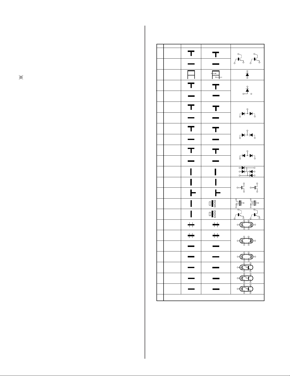
G
D
S
B1 E1
C2
B2 C1E2
2
3
4
5
6
7
8
9
0
!¡
!™
!¢
!§
!¶
!•
–
1
G
D
S
B2 E2
C1
B1 C2
E1
B2 E2
C1
B1 C2E1
B2 E2
C1
B1 C2E1
!ª
B1 E1
E2
C1(B2)
C2
@º
B1
E2
C1
C2
@™
@£
(B2)
E1
(B2)
E1
E2
B1
C2
C1
@¡
B1
E1
C2
B2
C1
E2
G
S
S
D
G
D
B1
E1
C2
B2
C1
E2
B1
E2
C2C1(B2)
E2
B1
C1
C2E1(B2)
C2
B1
C1
E2E1(B2)
C2
B1
C1
E2
B2
E1
C2
Ver.1.6
Transistor
(FET)
Transistor
Transistor
Transistor
Transistor
Transistor
Transistor
Transistor
Transistor
Transistor
Discrete semiconductot
(Chip semiconductors that are not actually used are included.)
Diode
Diode
Diode
Diode
Diode
Diode
Diode
Diode
Diode
Diode
Source
Source
Anode
Anode
(NC)
(NC)
Cathode
Anode
Cathode
Common
Cathode
Cathode
Common
Cathode
Cathode
Common
Common
Common
Common
Cathode
Anode
Base
Emitter
Collector
Base
Emitter
Collector
Drain
Gate
Gate
Drain
Device Printed symbol Terminal name
Circuit
Terminal name of semiconductors in silk screen
printed circuit ( )
Anode
Anode
Anode Cathode
Anode Anode
Cathode
!£
Transistor
(FET)
Transistor
(FET)
!?
Emitter
Collector
Base
Transistor
Source
Gate
Drain
Cathode
Anode
Anode
Cathode
Anode
Anode
*
REFERENCE INFORMATION
RESISTOR
: RN METAL FILM
: RC SOLID
: FPRD NONFLAMMABLE CARBON
: FUSE NONFLAMMABLE FUSIBLE
: RW NONFLAMMABLE WIREWOUND
: RS NONFLAMMABLE METAL OXIDE
: RB NONFLAMMABLE CEMENT
: ADJUSTMENT RESISTOR
COIL
: LF-8L MICRO INDUCTOR
CAPACITOR
: TA TANTALUM
: PS STYROL
: PP POLYPROPYLENE
: PT MYLAR
: MPS METALIZED POLYESTER
: MPP METALIZED POLYPROPYLENE
: ALB BIPOLAR
: ALT HIGH TEMPERATURE
: ALR HIGH RIPPLE
KLV-40W300A/46W300A/52W300A
24
KLV-40W300A/46W300A/52W300A
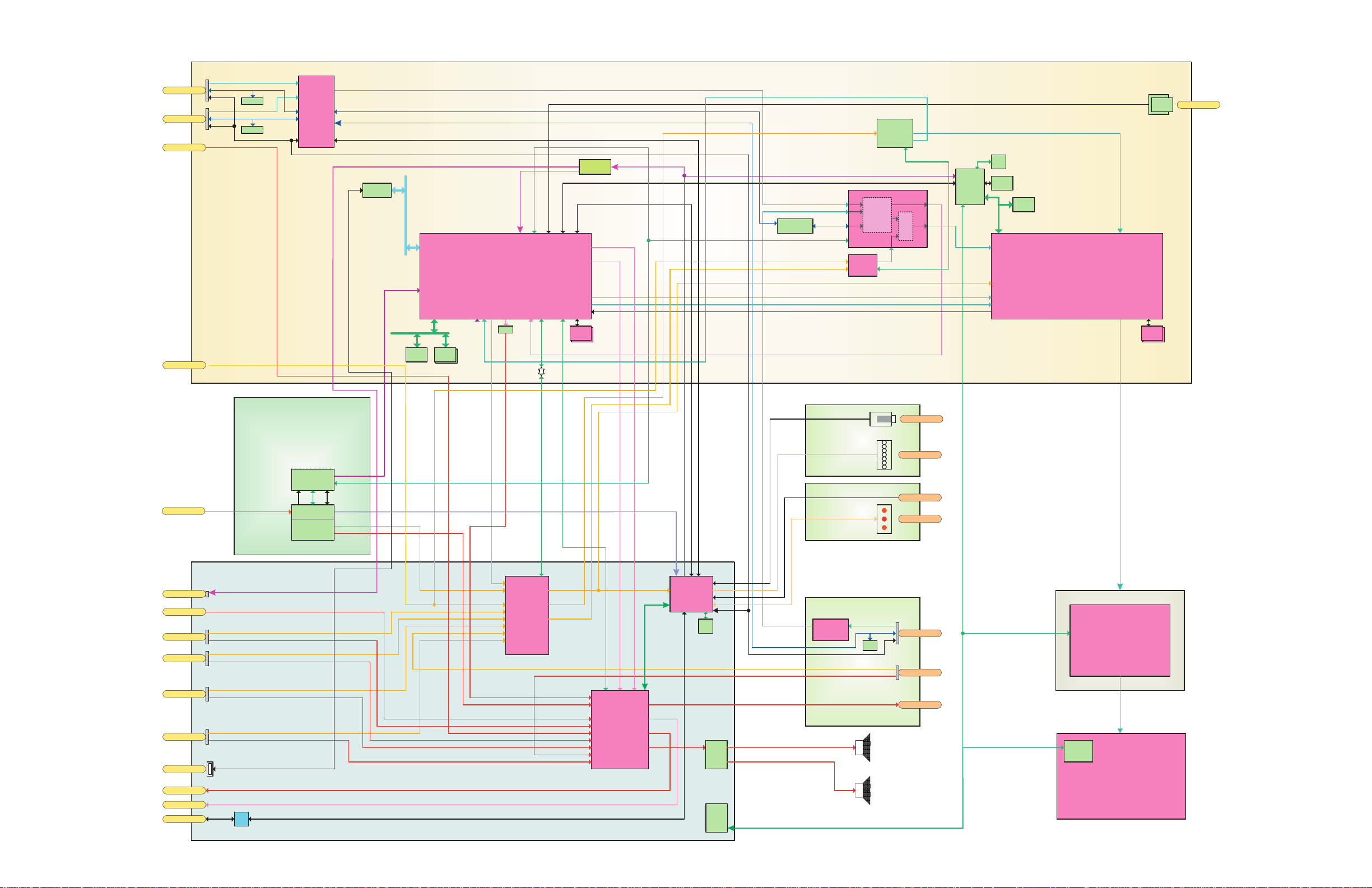
3-3. BLOCK DIAGRAM
HDM I I N 1
HDMI
Equalizer
CXB1444
NVM2KB
EDID
USB2.0
(HS)
uPD720101
HDM I I N 3
USB
DDC1
DDC3
DDC
TMDS1
TMDS3
TMDS
NVM2KB
EDID
Sel.
SN74LV4053
X2
Audio IN
Audio L/ R
EMMA2TH
DDR2
SDRAM
512Mbit x2
DDR2
SDRAM
512Mbit x2
NOR
2Mbit
NAND
32MB x2
NAND
64MB x2
RF- 1
EPP
Componennt2
SVide o1
Componennt1
Analog Y/Cb/ Cr
Audio L/ R
Audio L/ R
Analog CVBSY/C
Audio L/ R
Analog Y/Cb/ Cr
Video3
Analog CVBS
RS232C
Video
SW1
CXA2239
14 Input
5Output
Audio DSP
TAS 3208
D-
Modem
Sub15
Analog RGB H/V
AudioMini
PCI
TS
Sub Chroma
CCP- XA
I2S
BE Micro
Main
Gfx
H/ V
DA
SPD IF
I2S(5.1ch)
UART
Audio L/ R
Audio L/ R
CVBS/YC
CVBS/Y C/YCbCr
YCbCr/ RGB
DDC
Flash
EEP
DDR2
SDRAM
256Mbit x2
DDR2
SDRAM
256Mbit x2
Full HD
S-PVA
CCFL BackLight
40”, 46”, 52”
LCD-Panel
LB
Micro
T-Con
Sub Micro
Rigel
L/R OUT
Opt. OUT
I2C
UART
Audio L/ R
SPD IF
MS Service
MS D/L
Demodulator
8VSB/6 4QAM
256QAM/QPSK
Tuner(Main)
Demodulator
NTSC/ BTSC
Analog CVBS
Audio L/ R
Local Bus
Buff
Power
AM
TEMP
P
I2C
I2C
I2C
I2C
I2C I2C
I2C
I2C
CEC
CEC
UART
SDRAM
64Mb
EEP
I2C
I2C
I2C
I2C
HDMI IN2
HDMI
Equalizer
CXB1443
NVM
2KB
EDID
DDC2
TMDS2
USB
HP OUT
Video2
Analog CVBS
Audio L/ R
Power Sw.
LED
KEY
LED control
KEYcontrol
CEC
SIRCS
HW1
HW3
HW2
T- Con
AU
TUU2
FB1
I2C GPIOFAT
10bitA DC
Bus
SW
I2C
HDMIRx
V1.3
I2C
3-5
SPI
(DL)
SPI(D L)
Sensor
H_SYNC
SW(Buffer)

KLV-40W300A/46W300A/52W300A
25
KLV-40W300A/46W300A/52W300A
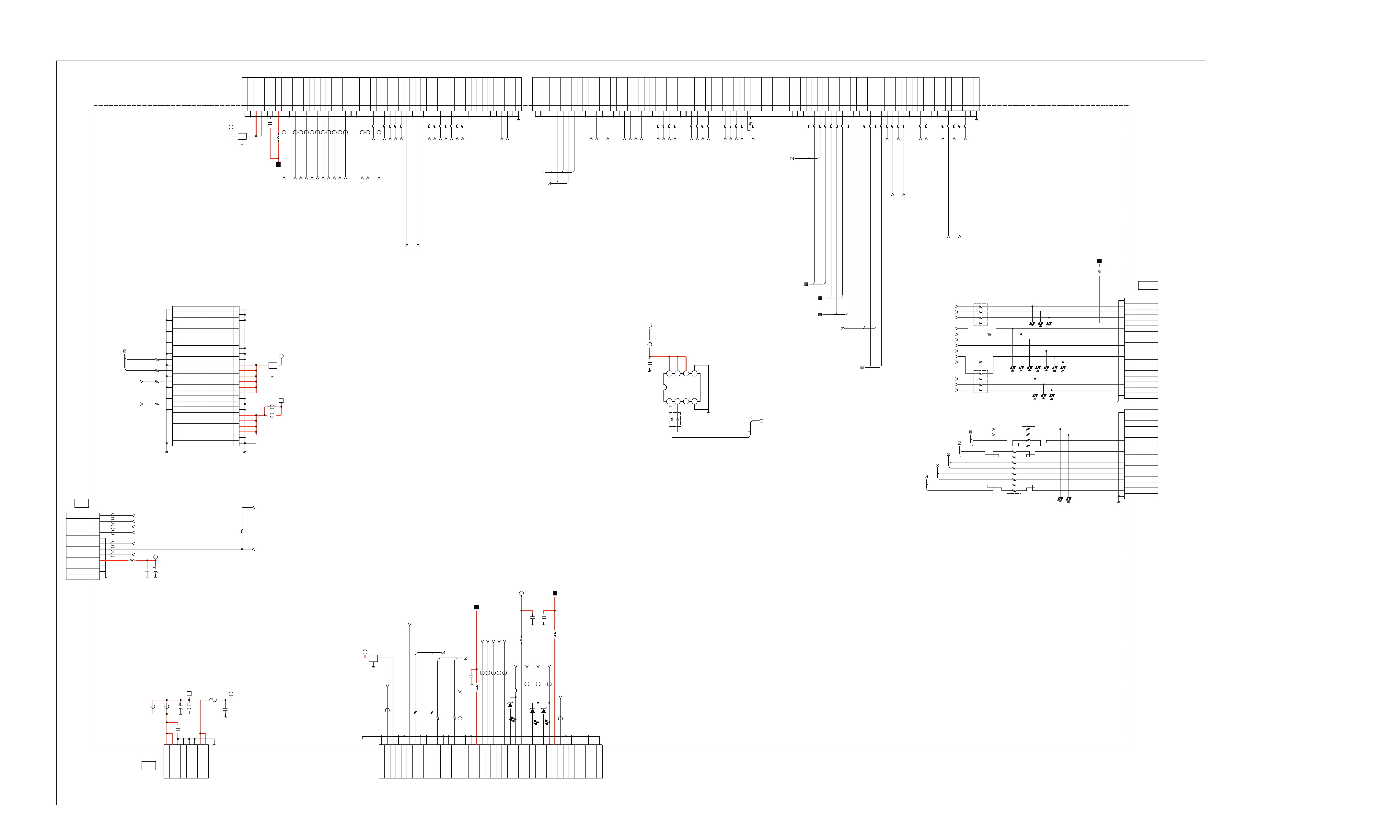
3-3-1. CONNECTOR DIAGRAM (KLV-40W300A ONLY)
㪚㪥㪎㪇㪇㪈
㪚㪥㪌㪍㪇㪈 㪚㪥㪋㪊㪇㪉
㪚㪥㪍㪎㪇㪎㩿㪋㫇㪀 㪣㪭㪛㪪㪄㪌㪈㪧
㪚㪥㪍㪎㪇㪏
㩿㪊㫇
㪀
㩷㪚㪥㪍㪎㪇㪈
㪚㪥㪌㪍㪇㪇
㪚㪥㪍㪍㪇㪇 㪚㪥㪍㪎㪇㪍
㩷㩷㩷㪚㪥㪉㪎㪇㪈
㪚㪥㪉㪐㪇㪇
㪝㪝㪚㪄㪋㪐㫇
㪚㪥㪍㪌㪇㪉 㪚㪥㪍㪈㪌㪊 㪝㪝㪚㪄㪋㪐㫇
㪚㪥㪈㪍㪇㪉
㪚㪥㪈㪇㪇㪊 㪚㪥㪇㪇㪈
㪚㪥㪍㪈㪌㪇 㪚㪥㪏㪇㪈
㪚㪥㪍㪈㪌㪋 㪚㪥㪇㪇㪉
㪚㪥㪍㪈㪌㪉 㩷㩷㩷㪚㪥㪇㪇㪋
㪣㪭㪛㪪㪄㪉㪈㫇
㩷㩷㩷㩷㪚㪥㪎㪇㪍㪈
㪚㪥㪎㪈㪌㪉
㩷㪚
㪚㪥㪎㪇㪉㪉
㪛㪝㪈
㩷㩷
㪞㪝㪈
㩷
㪟㪮㪊
㩷
㪟㪮㪈
㪟㪮㪉
㩷㩷㩷㩷
㪪㪧
㩷㩷㩷
㪪㪧
㪝㪙㪈
㩷㪝㪠㪯㪉㪄㪮㪋㪇
㪫㩷㪺㫆㫅
㪘㪬
㪫㪬㪬㪉
䇭㪙㪸㫃㪸㫅㪺㪼㫉㩷㪙㫆㪸㫉㪻

KLV-40W300A/46W300A/52W300A
26
KLV-40W300A/46W300A/52W300A
3-3-2. CONNECTOR DIAGRAM (KLV-46W300A ONLY)
㪚㪥㪎㪇㪇㪈 㩷㩷㪚㪥㪍㪐㪇㪇 㪚㪥㪍㪐㪇㪊
㪚㪥㪍㪐㪇㪋
㩷㩷㩷㪚㪥㪍㪏㪇㪇
㪚㪥㪍㪎㪇㪎
㩿㪋㫇㪀
㩷㩷㪚㪥㪍㪎㪇㪈 㩷㩷㩷㪚㪥㪌㪍㪇㪈
㪚㪥㪍㪎㪇㪏
㩿㪊㫇㪀
㪣㪭㪛㪪㪄㪌㪈㪧 㪚㪥㪋㪊㪇㪉
㪚㪥㪍㪎㪇㪋
㪚㪥㪌㪍㪇㪇
㪚㪥㪍㪍㪇㪇 㪚㪥㪍㪎㪇㪍
㪚㪥㪉㪐㪇㪇
㩷㩷㪚㪥㪉㪎㪇㪈
㪝㪝㪚㪄㪋㪐㫇
㪚㪥㪍㪌㪇㪉 㪚㪥㪍㪈㪌㪊
㩷㩷㪚㪥㪍㪌㪇㪈 㪚㪥㪈㪇㪇㪊 㪚㪥㪈㪍㪇㪉
㪚㪥㪇㪇㪈
㪚㪥㪍㪈㪌㪇
㪚㪥㪍㪈㪌㪋
㪚㪥㪏㪇㪈
㪚㪥㪍㪈㪌㪉 㪚㪥㪇㪇㪉 㩷㩷㩷㩷㪚㪥㪇㪇㪋
㪣㪭㪛㪪㪄㪉㪈㫇
㩷㩷㩷㩷㪚㪥㪎㪇㪍㪈
㪚㪥㪎㪈㪌㪉
㩷㪚
㪚㪥㪎㪇㪉㪉
㪛㪝㪉
㩷㩷
㪞㪝㪈
㩷
㪟㪮㪊
㩷
㪟㪮㪉
㩷㩷㩷㩷
㪪㪧
㩷㩷㩷㩷
㪪㪧
㪝㪙㪈
㩷㪝㪠㪯㪉㪄㪮㪋㪍
㪛㪝㪊
㩷
㪟㪮㪈
㪫㩷
㪘㪬
㪫㪬㪬㪉
䇭㪙㪸㫃㪸㫅㪺㪼㫉㩷㪙㫆㪸㫉㪻
䇭㪙㪸㫃㪸㫅㪺㪼㫉㩷㪙㫆㪸㫉㪻

KLV-40W300A/46W300A/52W300A
27
KLV-40W300A/46W300A/52W300A
3-3-3. CONNECTOR DIAGRAM (KLV-52W300A ONLY)
㪚㪥㪎㪇㪇㪈 㩷㩷㪚㪥㪍㪌㪇㪊 㪚㪥㪍㪌㪇㪌
㪚㪥㪍㪌㪇㪋
㩷㩷㪚㪥㪍㪋㪇㪇
㪚㪥㪍㪎㪇㪎㩿㪋㫇㪀 㩷㩷㩷㩷㪚㪥㪍㪎㪇㪈 㩷㩷㩷㪚㪥㪌㪍㪇㪈
㪚㪥㪍㪎㪇㪏㩿㪊㫇㪀 㪣㪭㪛㪪㪄㪌㪈㪧 㪚㪥㪋㪊㪇㪉
㪚㪥㪍㪎㪇㪋 㪣㪭㪛㪪㪄㪉㪈㫇
㪚㪥㪌㪍㪇㪇
㪚㪥㪍㪍㪇㪇 㪚㪥㪍㪎㪇㪍
㪚㪥㪉㪐㪇㪇
㩷㩷㩷㪚㪥㪉㪎㪇㪈
㪝㪝㪚㪄㪋㪐㫇
㪚㪥㪍㪌㪇㪉 㪚㪥㪍㪈㪌㪊
㩷㩷㪚㪥㪍㪌㪇㪈 㪚㪥㪈㪇㪇㪊 㪚㪥㪈㪍㪇㪉
㪚㪥㪇㪇㪈
㪚㪥㪍㪈㪌㪇
㪚㪥㪏㪇㪈
㪚㪥㪍㪈㪌㪋
㪚㪥㪍㪈㪌㪉 㪚㪥㪇㪇㪉 㩷㩷㩷㪚㪥㪇㪇㪋 㩷㩷㪣㪭㪛㪪㪄㪉㪈㫇
㩷㩷㩷㩷㪚㪥㪎㪇㪍㪈
㪚㪥㪎㪈㪌㪉
㩷㪚
㪚㪥㪎㪇㪉㪉
㩷㩷
㪛㪝㪋
㩷㩷
㪞㪝㪉
㩷
㪟㪮㪊
㩷
㪟㪮㪉
㩷㩷㩷㩷㩷㩷
㪪㪧
㩷㩷㩷㩷
㪪㪧
㪝㪙㪈
㩷㪝㪠㪯㪉㪄㪌㪉㪮
㩷㩷
㪛㪝㪌
㩷
㪟㪮㪈
㪫㩷㪺㫆㫅
㪘㪬
㩷
㪫㪬㪬㪉
䇭㪙㪸㫃㪸㫅㪺㪼㫉㩷㪙㫆㪸㫉㪻
䇭㪙㪸㫃㪸㫅㪺㪼㫉㩷㪙㫆㪸㫉㪻
KLV-40W300A/46W300A/52W300A
KLV-40W300A/46W300A/52W300A 28
1 | 2 | 3 | 4 | 5 | 6 | 7 | 8 | 9 | 10 | 11 | 12 | 13 | 14 | 15 | 16 | 17 | 18 | 19 | 20 | 21 | 22 | 23 | 24 | 25
A
—
B
—
C
—
D
—
E
—
F
—
G
—
H
—
I
—
J
—
K
—
L
—
M
—
N
—
O
—
P
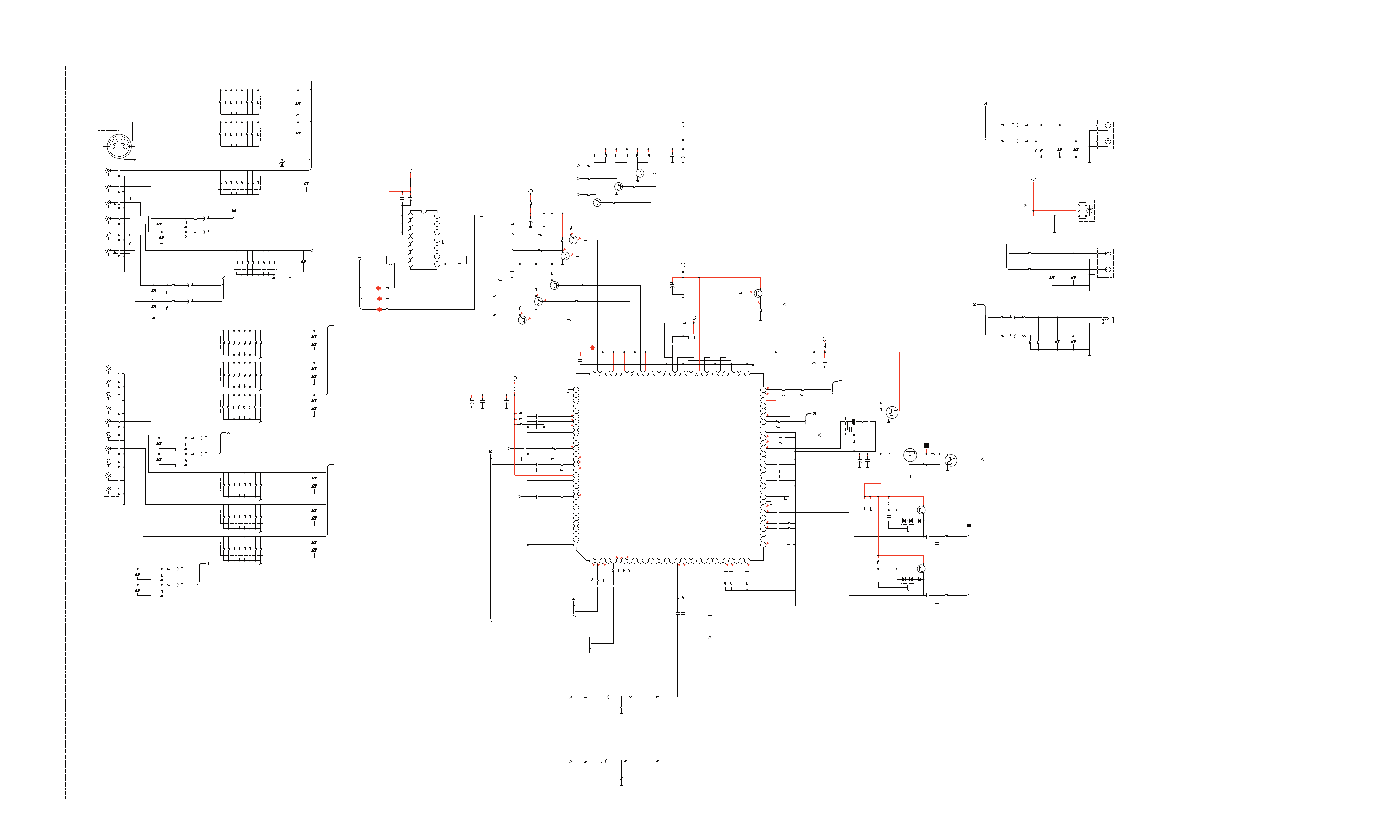
AU BOARD SCHEMATIC DIAGRAM (1 OF 6)
3-4. SCHEMATICS AND SUPPORTING INFORMATION
REC3.3V
0uH
FB006
V_DET
TV_M_LR_IN
004:7D
POWER_LED
STBY_LED
REC_LED
REC3.3V
KEY1
SIRCS
POWER_SW
ON_TIMER_LED
BL_IN
PMUTE_LED
AUDIO_VCC
EMI
G
FL001
TUHSYNC_MAIN
0uH
FB008
0uH
FB011
0uH
FB010
0uH
FB009
0uH
FB007
0uH
FB015
0uH
FB014
0uH
FB012
CHIP
R133 0
EMI
G
FL002
REC6.5V
12V
1
2
3
4
5
6
7
8
8P
CN002
12V
12V
GND
GND
GND
GND
AUDIO_VCC
AUDIO_VCC
0uH
FB001
12V
STBY3.3V
REC5V
R014
0
R016
0
R012
0
R013
0
FE_I2C_2
BEM_I2C_1
BEM_I2C_2
BEM_I2C_3
FE_I2C_0
TV_TXD
TV_RXD
BEM_TX0
BEM_RX0
MODE_BEM
EMMA_LOG_TX
BEM_RST
LBM_DMNS
LBM_VBUS
LBM_DPLS
EMMA_LOG_RX
JIG_RST
BEM_RX3
BEM_TX3
LOGO
HP_LR_OUT
V2_V_IN
HP_DET
001:8E
0
R031
0
R035
V2_LR_IN
0
R037
0
R028
STBY5V
22
R115
22
R117
DIMMER
BALLANCER_ERR
PFC_DET
BL_ON
STBY5V
AC_RLY
INV_FAIL
+B_OVP
BEM_I2C_2
TV_FLASH_M
AC_DET
1005
CHIP
R026
0
1005
50V
0.001
X7R
C005
1005
16V
0.1
C009
16V
470
C003
16V
470
C004
BE_ON
1
2
3
4
5
6
7
8
9
10
11
12
13
14
15
16
BLK
16P
CN008
GND
AVC_LOG(TX)
AVC_LOG(RX)
BEM_LOG(TX)
BEM_LOG(RX)
E2TH_SCL_0(400)
E2TH_SDA_0(400)
BEM_SCL_1(400)
BEM_SDA_1(400)
BEM_SCL_2(100)
BEM_SCL_2(100)
BEM_SCL_3(400)
BEM_SDA_3(400)
E2TH_SCL_2_VSW
E2TH_SDA_2_VSW
GND
BE_FAN_DRV1
EMMA2_AOLRCK
R091
0
BE_FAN_DRV2
MAIN_H_SYNC
R059
0
BALLANCER_ERR
AC_DET
EMMA_LOG_TX
R050
0
SPI_SCK
R084
0
BEM_TX0
R096
0
EMMA2_AOMCK
R058
0
FE_I2C_2
HDMI_DSP_MUTE2
HDMI_HOTPLUG_CTRL
R034
0
R098
0
DIMMER
R078
0
R079
0
R029
0
DTT_WDT
CEC_ON
BEM_RX3
R033
0
R062
0
PC_V_IN
R085
0
R060
0
MAIN_V_OUT
HDMI_STBY3.3V
EMMA_LOG_RX
REC5V-BE
BEM_TX3
BEM_I2C_1
R110
0
MODE_BEM
R075
0
HDMI_SEL_4
R090
0
I2C_TAS_SDA_1
LBM_DMNS
R046
0
R081
0
EMMA2_AOBCK
I2C_TAS_SCL_1
SPI_SI
R092
0
LBM_DPLS
R041
0
R094
0
HDMI_SEL_2
R056
0
EMMA2_AOD0
R108
0
BE_ON2
CEC_IN
R109
0
R061
0
EMMA_SPDIF
R030
0
HDMIPC_WP
R071
0
S_CR
EMMA2_AOD2
S_Y/CV
BL_IN
MAIN_COMP_OUT
DSP_INT
PC_H_IN
REC_ON
BE_ON
R104
0
BEM_RST
FE_I2C_0
R039
0
R036
0
R032
0
BE_WDT
BEM_I2C_3
PC_V_OUT
R057
0
R074
0
LBM_VBUS
PC_H_OUT
R093
0
DDC5V_DET_0
HDMI_SEL_1
R027
0
TV_EMMA_UART
BE_RST
S_C
R048
0
INV_FAIL
R087
0
R080
0
BEM_I2C_2
R073
0
R083
0
EMMA2_AOD1
DDC5V_DET_1
HP_DET
BL_ON
HDMI_SEL_3
EMI
G
FL003
R105
0
R086
0
R077
0
BEM_RX0
R076
0
DL_CS
R088
0
CEC_OUT
R089
0
1005
50V
X7R
C017
0.001
0uH
FB016
0uH
FB022
0uH
FB018
0uH
FB021
0uH
FB019
0uH
FB017
0uH
FB020
1005
50V
0.001
X7R
C001
1005
50V
X7R
C018
0.001
0uHFB002
1005
50V
0.001
X7R
C010
0uH
FB023
0uH
FB044
1005
50V
0.001
X7R
C014
0.001C013
0uH
FB032
0uH
FB037
0uH
FB029
0uH
FB028
0uH
FB025
0uH
FB036
0uH
FB033
0uH
FB026
0uH
FB034
0uH
FB031
0uH
FB027
FB024
0uH
0uH
FB030
0uH
FB035
REC_Y
REC_C
0.001
C019
1005
CHIP
*R106
0
22
RB001
22
RB002
22
RB003
22
RB004
0uH
FB045
0uH
FB046
0uH
FB047
0uH
FB048
0uH
FB051
1
2
3
4
5
6
7
8
9
10
11
12
12P
CN001
WHT
BALLANCER_ERR
INV_ERR
BL_ON
DIMMER
GND
AC_RLY
PFC_DET(AC_DET)
PS_ERR
STBY_5V
GND
GND
18V
1
2
3
4
5
6
7
8
9
10
11
12
13
14
15
16
17
18
19
20
21
22
23
24
25
26
27
28
29
30
31
32
33
34
35
36
37
38
39
40
40P
CN004
NC
BE_ON
REC5V
GND
GND
V2_V
V2_L
GND
GND
V2_R
HP_L
GND
GND
HP_R
HP_DET
GND
GND
STBY3.3V
LED_1(STBY)
LED_2(PMUTE)
LED_3(TSUSHIN)
LED_4(REC)
VED_5(POWER)
GND
SIRCS
REC_3.3V
BL_IN
NC
POWER_SW
GND
KEY
STBY5V
LOGO
GND
NC
STBY3.3V
IRO
GND
SET3.3V
NC
22
RB005
VD016
VD019
VD023
VD026
VD030
VD017
VD020
VD024
VD025
VD028
VD018
VD021
VD022
VD027
VD029
24V
5A
F001
12
3
5
7
9
11
13
15
17
19
21
23
25
27
29
31
33
35
37
39
41
43
45
47
4
6
8
10
12
14
16
18
20
22
24
26
28
30
32
34
36
38
40
42
44
46
48
5049
BRN
50P
CN003
GND
TV_S_L
GND
TV_S_R
GND
SUB_H
GND
TV_S_V
GND
TV_M_L
GND
TV_M_R
GND
MAIN_H
GND
TV_M_V
GND
TV_GR_V
GND
FE_XRST
EWS_ALERT
AGC_MON
REC_ON
EWS_ON
REC_3.3V
GND
GND
GND
REC_6.5V
REC_6.5V
REC_6.5V
REC_6.5V
REC_6.5V
REC_6.5V
GND
GND
GND
12V
12V
12V
12V
GND
GND
GND
GND
REC_3.3V
REC_3.3V
REC_3.3V
GND GND
0uH
FB052
0uH
FB053
0uH
FB038
8765
4321
ADT75ARZ-REEL
IC001
6.3V
220
C002
1
2
3
4
5
6
7
8
9
10
11
12
13
14
15
16
17
18
19
20
21
22
23
24
25
26
27
28
29
30
31
32
33
34
35
36
37
38
39
40
41
42
43
44
45
46
47
48
49
50
BLK
50P
CN005
GND
GND
REC5V
REC5V
GND
GND
STBY3.3V
AC_DET
GND
BL_ON
DIMMER
INV_FAIL1
BALLANCER_ERR
BL_IN
HP_DET
DSP_INT
DSP_MUTE2
DTT_PON
HDMI_WP
GND
GND
SET_ON2
SET_ON
BE_WDT
BE_RST
DDC_DET2
X_WDTRST
HPG_CTL
DDC_DET1
FE_SCL1
GND
FE_SDA1
GND
FE_SPDIF
EMMA2_AOBCK
EMMA2_AOLRCK
EMMA2_AOMCK
EMMA2_AOD2
EMMA2_AOD0
EMMA2_AOD1
GND
GND
ASUB_R
ASUB_L
GND
GND
REC_Y
REC_C
GND
GND
1
2
3
4
5
6
7
8
9
10
11
12
13
14
15
16
17
18
19
20
21
22
23
24
25
26
27
28
29
30
31
32
33
34
35
36
37
38
39
40
41
42
43
44
45
46
47
48
49
50
51
52
53
54
55
56
57
58
59
60
61
62
63
64
65
66
67
68
69
70
71
72
73
74
75
76
77
78
79
80
BLK
80P
CN006
GND
GND
M_YS
M_CB/B
M_CV/Y
M_CR/R
M_C
M_Y/G
GND
GND
S_C
S_CR
GND
S_CV/Y
GND
GND
PC_H_OUT
PC_V_OUT
PC_H_IN
PC_V_IN
GND
GND
EPP(CCPM)_HS
DL_SI
DL_SCK
DL_CS
GND
GND
HDMI_INSEL2
HDMI_INSEL1
HDMI_INSEL4
HDMI_INSEL3
HDMI_SCL
HDMI_SDA
CEC_IN
CEC_OUT
CEC_ON
FAN_DRIVE1
FAN_ERR
FAN_DRIVE2
X_MDM_RST
UART2_DCD
UART2_RST
UART2_CTS
UART2_TX
UART2_RX
GND
GND
GND
TV_EMMA_TX
FE_SCL0
TV_EMMA_RX
FE_SDA0
BEM_SDA3
BEM_SDA2
BEM_SCL3
BEM_SCL2
GND
GND
BEM_SCL1
FE_SDA2
BEM_SDA1
FE_SCL2
EMMA_LOG_TX
BEM_TX3
EMMA_LOG_RX
BEM_RX3
GND
GND
LBM_DPLS
LBM_DMNS
GND
GND
LBM_VBUS
BEM_TX0
BEM_RST
BEM_RX0
MODE_BEM
GND
GND
1
2
3
4
5
6
7
8
9
10
11
12
13
14
15
16
17
18
18P
CN007
GND
TV_TXD
TV_RXD
TV_FLASH_W
STBY3.3V
TV_RST
DTT_LOG_RXD
LBM_UDP
LBM_UDM
LBM_VBUS
BEM_RST
DTT_LOG_TXD
NC
NC
BE_FLASH_W
BEM_RXD
BEM_TXD
GND
STBY3.3V
0
R146
MAZ8056G0LS0D017
MAZ8056G0LS0
D019
MAZ8056G0LS0
D018
VD031
VD032
VD033
TV_M_R
V2_L
V2_R
HP_L
HP_R
TV_M_L
M_CR/R
M_Y/CV
M_Y/G
BEM_SCL3
BEM_SCL1
M_C
FE_SDA0
M_CB/B
TV_EMMA_TX
TV_EMMA_RX
FE_SDA2
FE_SCL2
BEM_SDA3
BEM_SCL3
BEM_SDA2
BEM_SDA1
BEM_SCL1
BEM_SCL2
FE_SDA0
FE_SCL0
BEM_SCL2
BEM_SDA2
FE_SCL0
BEM_SDA1
To G
To TUU2
To G
To JIG
CN7001
TO HW1 BOARDTO HW2 BOARD
CN7022
TO HW3 BOARD
CN7152
TO GF1 BOARD
CN6154
TO GF1 BOARD
CN6152
CN1001
A-1231-638-B <FIX2>AU-P1
CONNECTORS
AU 1/6
CN4001
TO FB1 BOARD
CN4002
TO FB1 BOARD

KLV-40W300A/46W300A/52W300A
KLV-40W300A/46W300A/52W300A 29
1 | 2 | 3 | 4 | 5 | 6 | 7 | 8 | 9 | 10 | 11 | 12 | 13 | 14 | 15 | 16 | 17 | 18 | 19 | 20 | 21 | 22 | 23 | 24 | 25 |
A
—
B
—
C
—
D
—
E
—
F
—
G
—
H
—
I
—
J
—
K
—
L
—
M
—
N
—
O
—
P
AU BOARD SCHEMATIC DIAGRAM (2 OF 6)
3216
25V
4.7
X7R
C202
1/16W
CHIP
10k
R204
1/16W
CHIP
10k
R207
REC_ON
REC3.3V
1/16W
CHIP
10k
R201
25V
1
C241
2012
1/16W
CHIP
1k
R274
5%
1/16W
CHIP
1k
R273
5%
12345
PQ070XNA1ZPH
IC207
Vin
Vc
Vo
Vadj
GND
25V
1
C240
2012
12345
PQ070XNA1ZPH
IC206
Vin
Vc
Vo
Vadj
GND
REC5V-BE
1/16W
RN-CP
1k
R294
0.5%
CHIP
0
R283
1/16W
CHIP
10k
R287
1/16W
RN-CP
4.7k
R291
0.5%
CHIP
0
R289
1/16W
RN-CP
1k
R293
0.5%
REC_ON
25V
4.7
C254
X7R
3216
12345
PQ200WNA1ZPH
IC208
Vin
Vc
Vo
Vadj
GND
2012
25V
1
C248
1/16W
CHIP
10k
R281
3216
25V
4.7
X7R
C252
1/16W
RN-CP
100
R292
0.5%
1005
R299
0
1608
0
R269
1608
0
R270
1608
0
R271
1608
0
R272
FB206
0
R233
D205
MA24D5000BS0
1/16W
RN-CP
8.2k
R237
0.5%
JL213
1608
16V
1
C224
B
0
R262
8765
4321
RSS040P03FD5TB
Q207
1234
5678
1005
16V
0.015
B
C227
JL212
3216
25V
4.7
X7R
C208
10k
R246
JL202
GND_1
0
R249
12V
12V
REC5V
REC6.5V
SET9V
PTZ-TE25-6.8B
D212
3216
25V
4.7
X7R
C231
10uH
L203
1/16W
CHIP
5%
1k
R206
1608
50V
C229
B
3300p
1608
50V
C230
B
3300p
1608
RN-CP
R260
1/10W
5%
15
1608
RN-CP
R259
1/10W
5%
15
1608
RN-CP
R252
1/10W
5%
15
3216
10V
X7R
C245
10
3216
10V
X7R
C244
10
2012
25V
1
C223
1608
16V
1
C220
B
1/16W
RN-CP
47k
R267
0.5%
1/16W
RN-CP
270k
R266
0.5%
1/16W
RN-CP
43k
R265
0.5%
REC9V
RT1N141C-TP-1
Q210
1005
50V
680p
B
C228
1005
50V
22p
CH
C233
1/16W
RN-CP
10k
R258
0.5%
1/16W
RN-CP
0.5%
56k
R268
RN-CP
R275
2.7k
1/16W
0.5%
RN-CP
R276
390
1/16W
0.5%
RN-CP
R277
1k
1/16W
0.5%
RN-CP
R278
2.7k
1/16W
0.5%
RN-CP
R279
390
1/16W
0.5%
RN-CP
R280
1k
1/16W
0.5%
TAS3.3V
12345
PQ070XNA1ZPH
IC210
Vin
Vc
Vo
Vadj
GND
RN-CP
R305
1k
1/16W
0.5%
1608
CHIP
R300
0
RN-CP
R304
1k
1/16W
0.5%
1608
CHIP
R301
0
1/16W
CHIP
1k
R302
5%
25V
1
C257
2012
2SC3052EF-T1-LEF
Q212
24V
3.15A
F201
MAZ8068G0LS0
D201
RT3WLMM-TP-1F
Q214
CHIP
0
R251
CHIP
0
R218
TAS3.3V
CHIP
0
R306
CHIP
0
R307
16V
47
C261
RN-CP
R303
680
1/16W
0.5%
FB202
0uH
10V
C259
10
X7R
3216
16 15 14 13 12 11
10 9
87
654321
IC205
BD9853AFV
Vcc
OUT1_1
OUT1_2
VB
RT
FB1
-INE1
CSCP1 CSCP2
-INE2
FB2
GND
CTL
OUT1_2
OUT2_1
VH
1608
CHIP
*R308
0
REC9V
REC5V-B
E
REC3.3V
REC5V
REC6.5V
SET9V_2
3.15A
TAS3.3V
A-1231-638-B
AU 2/6
POWER REGS
<FIX2>AU-P2
KLV-40W300A/46W300A/52W300A
KLV-40W300A/46W300A/52W300A 30
1 | 2 | 3 | 4 | 5 | 6 | 7 | 8 | 9 | 10 | 11 | 12 | 13 | 14 | 15 | 16 | 17 | 18 | 19 | 20 | 21 | 22 | 23 | 24
A
—
B
—
C
—
D
—
E
—
F
—
G
—
H
—
I
—
J
—
K
—
L
—
M
—
N
—
O
—
P
AU BOARD SCHEMATIC DIAGRAM (3 OF 6)
1/16W
100R522
1/16W
CHIP
5%
68k
R552
1/16W100
R494
1/16W
100
R530
1/16W
100
R492
S
SI2301BDS-T1
Q420
1/16W
R509
100
VSW_PW_CTRL
1/16W
CHIP
5%
47
R578
1/16W
100
R531
1/16W
CHIP
5%
10k
R594
FE_I2C_2
1/16W
CHIP
5%
68k
R553
PC_SYNC_INT
1/16W
CHIP
5%
47
R579
1/16W100
R495
1/16W
100R498
1/16W
100
R493
1/16W
100
R508
PC_SYNC_OUT
1/16W
100
R507
D1_V_IN
V1_IN
D2_V_IN
MAIN_V_OUT
1/16W
CHIP
22
R481
1/10W
RN-CP
330
R486
5%
1/10W
RN-CP
330
R478
5%
1/16W
CHIP
22
R475
1/10W
RN-CP
330
R474
5%
1/16W
CHIP
22
R512
1/16W
CHIP
22
R516
1/10W
RN-CP
330
R511
5%
1/10W
RN-CP
330
R515
5%
1/16W
CHIP
22
R517
1/16W
CHIP
5%
22
R546
1/16W
CHIP
5%
22
R548
MAIN_COMP_OUT
2SA1226-T1E3E4
Q407
2SA1226-T1E3E4
Q403
2SA1226-T1E3E4
Q406
V2_V_IN
1/16W100R541
CHIP
0
R453
CHIP
0
R510
1005
16V
0.1
C504
14 13 12 11 10 9
8
7
654321
ADA4861-3YRZ-RL7
IC401
PD1
PD2
PD3
VCC
IN+1
IN-1
OUT1 OUT3
IN-3
IN+3
VEE
IN+2
IN-2
OUT2
RN-CP
R461
470
1/10W
0.5%
RN-CP
R455
470
1/10W
0.5%
RN-CP
R451
470
1/10W
0.5%
R572
0
R573
0
1/16W330k
R471
1/16W330k
R472
1/16W330k
R473
1005
CHIP
R589
0
4MHz
X401
V3_V
V3_V
D2_LR_IN
V1_LR_IN
CHIP
0
R416
CHIP
0
R415
D1_V_IN
D2_V_IN
V3_LR_IN
D1_LR_IN
V1_IN
L
R
J403
CHIP
0
R597
PC_LR_IN
J404
CHIP
0
R598
OPT_OUT
LINE_LR_OUT
REC5V
HDMI_LR
L
R
J402
CHIP
0
R600
CHIP
0
R599
REC5V
REC5V
STBY5V
REC5V
REC5V
1/10W
RN-CP
0.5%
10
R476
1/10W
RN-CP
0.5%
10
R477
1/10W
RN-CP
0.5%
10
R465
1/10W
RN-CP
0.5%
10
R466
1/10W
RN-CP
0.5%
10
R467
S_C
S_Y/CV
S_CR
1/16W
CHIP
5%
22
R543
CHIP
0
R583
CHIP
0
R584
REC9V
SET9V
2012
25V
1
C450
2012
25V
1
C426
2012
25V
1
C464
1005
16V
0.1
C453
1005
16V
0.1
C471
1005
16V
0.1
C474
1005
16V
0.1
C499
1005
16V
0.1
C502
1608
10V
1
X7R
C508
1005
16V
0.1
C514
1608
10V1X7RC485
1608
10V
1
X7R
C487
1005
25V
0.01
X7R
C486
1005
25V0.01
X7RC488
1005
16V
0.1
C495
100516V
C494
0.1
16V
10
C404
16V
10
C405
16V
10
C412
16V
10
C413
16V
10
C406
16V
10
C407
16V
10
C408
16V
10
C409
16V
C517
10
16V
C518
10
16V
C515
10
16V
C516
10
16V
47
C419
16V
47
C470
16V
47
C500
RT1N141C-TP-1
Q423
1005
50V
47p
CH
C512
1005
16V
0.1
C503
1/16W
CHIP
5%
470
R595
Q421
2SC3052EF-T1-LEF
1005
25V
0.01
X7R
C505
1005
50V
47p
CH
C511
C506
0.01
25V
X7R
1005
1/16W
CHIP
5%
470
R596
Q422
2SC3052EF-T1-LEF
C507
0.01
25V
X7R
1005
3216
10V
10
X7R
C509
3216
10V
10
X7R
C510
RT1N141C-TP-1
Q419
1/16W
CHIP
5%
10k
R591
PC_SYNC_IN
10V
10
X7R
C489
10V X7R
C490 10
1/16WR613 100
1/16WR614 100
2SC3052EF-T1-LEF
Q424
1/16W
CHIP
5%
100
R615
1/16W
RN-CP
0.5%
1k
R616
DATA_SLICER_MAIN
V_DET
1608
25V
0.1
C418
X7R
160810V1X7RC432
160810V1X7RC433
160810V1X7RC434
201216V2.2 X7RC439
201216V2.2 X7RC440
201216V2.2 X7RC443
2012
16V2.2 X7R
C447
201216V2.2 X7R
C448
201216V2.2 X7R
C449
201216V2.2 X7R
C454
201216V2.2 X7R
C455
201216V2.2 X7R
C456
201216V2.2 X7R
C472
201216V2.2 X7R
C475
1608
25V
0.1
X7R
C473
1/16W
RN-CP
10kR574
0.5%
D422
MC2838-T112-1
D421
MC2838-T112-1
REC_Y
REC_C
201216V2.2 X7RC437
1/16W
CHIP100
R575
1/16W
CHIP
5%
1M
R424
1/16W
CHIP
5%
1M
R425
1/16W
CHIP
5%
1M
R439
1/16W
CHIP
5%
1M
R440
1/16W
CHIP
5%
1M
R427
1/16W
CHIP
5%
1M
R428
1/16W
CHIP
5%
1M
R429
1/16W
CHIP
5%
1M
R430
1/16W
CHIP
5%
1M
R602
1/16W
CHIP
5%
1M
R604
1/16W
CHIP
5%
1M
R601
1/16W
CHIP
5%
1M
R603
CHIP
0
R618
CHIP
0
R617
10uH
L403
10uH
L405
10uH
L407
MAZ8100G0LS0
D402
VIN
VCC
GND
BLK
3P
TB404
1/10W
RN-CP
0.5%
75
R627
1/10W
RN-CP
0.5%
75
R628
0
R629
0
R630
0
R631
0
R632
0
R633
0
R634
1/10W
RN-CP
270
R537
5%
1/10W
RN-CP
270
R542
5%
1/10W
RN-CP
270
R532
5%
1/10W
RN-CP
0.5%
39
R529
1/10W
RN-CP
0.5%
39
R527
1/10W
RN-CP
0.5%
39
R528
VD440
VD445
VD450
VD455
VD460
VD465
VD441
VD446
VD451VD456VD461
VD466
VD442
VD447
VD452VD457
VD462
VD467
VD443
VD448VD453VD458
VD463
VD468
VD444
VD449
VD454
VD459
VD464
VD469
MA2J1110GLS0
D423
MA2J1110GLS0
D424
ISA1235AC1TP-1EF
Q408
ISA1235AC1TP-1EF
Q414
ISA1235AC1TP-1EF
Q415
ISA1235AC1TP-1EF
Q409
ISA1235AC1TP-1EF
Q416
R590
10k
1/16W
CHIP
5%
R592
10k
1/16W
CHIP
5%
10uH
L406
1/10W
RN-CP
5%
270
R637
1/10W
RN-CP
5%
270
R638
1/10W
RN-CP
5%
270
R639
1608
25V0.1C438
X7R
1/10W
RN-CP
0.5%
2.2k
R431
1/10W
RN-CP
0.5%
2.2k
R432
1/10W
RN-CP
0.5%
2.2k
R433
1/10W
RN-CP
0.5%
2.2k
R435
1/10W
RN-CP
0.5%
2.2k
R436
1/10W
RN-CP
0.5%
2.2k
R437
1/10W
RN-CP
0.5%
2.2k
R441
1/10W
RN-CP
0.5%
2.2k
R442
1/10W
RN-CP
0.5%
2.2k
R443
1/10W
RN-CP
0.5%
2.2k
R444
1/10W
RN-CP
0.5%
2.2k
R445
1/10W
RN-CP
0.5%
2.2k
R446
1/16W
CHIP
5%
3.3k
R593
160816V1B
C478
RB401
600
RB402
600
RB403
600
RB404
600
RB405
600
RB406
600
RB407
600
RB408
600
RB409
600
RB410
600
3
4
12
L1
R1
V1
L2
R2
V2
TB401
12
34
5
6
7
8
9
10
11
12
14
15
16
17
13
18
19
20
GRN
BLU
RED
WHT
RED
GRN
BLU
RED
WHT
RED
J405
10V
100
C524
10V
100
C525
6.3V
220
C498
6.3V
220
C466
REC5V
10uH
L404
10V
100
C458
6.3V
1000
C425
6.3V
220
C526
1608
16V
0.068
B
C527
123456789101112131415161718192021222324252627282930
31
32
33
34
35
36
37
38
39
40
41
42
43
44
45
46
47
48
49
50
51
52
53
54
55
56
57
58
59
60
616263646566676869707172737475767778798081828384858687888990
91
92
93
94
95
96
97
98
99
100
101
102
103
104
105
106
107
108
109
110
111
112
113
114
115
116
117
118
119
120
CXA2240AR-TL
IC402
C/CB/B_IN8
Y/Y/G_IN8
CV/CR/R_IN8
MD3/S2-3
C/CB/B_IN7
Y/Y/G_IN7
CV/CR/R_IN7
S1-3
C/CB/B_IN6
Y/Y/G_IN6
CV/CR/R_IN6
MD2/S2-2
C/CB/B_IN5
Y/Y/G_IN5
CV/CR/R_IN5
S1-2
C/CB/B_IN4
Y/Y/G_IN4
CV/CR/R_IN4
S2-1
CV3
CV2
CV1
S1-1
IN1_L3
IN1_V/L2
IN1_H/L1
IN1_SW
IN2_L3
IN2_V/L2
IN2_H/L1
IN2_SW
IN3_L3
IN3_V/L2
IN3_H/L1
IN3_SW
IN4_V
IN4_H
GND_DEF
SYNC_OUT1
SYNC_IN1
H_PH1
V_PH1
SYNC_OUT2
SYNC_IN2
H_PH2
V_PH2
VCC_DEF
EXT_CLK/X’tal
PS_HVCS
IREF
GND5H_OUT
SELH_OUT1
SELV_OUT1
PC_ID
SELH_OUT2
SELV_OUT2
VCC5H_OUT
SDA
SCL
ADR
DC_OUT
C_OUT5
NC
Y_SAG
CV/Y_OUT5
NC
CV_SAG
CV_OUT5
VCC_9OUT
CV/Y_OUT4
CV/Y_OUT3
GND9_OUT
Y_PH2
Y_PH1
GND5_OUT
C/CB/B_OUT2
CV/Y/G_OUT2
C/CR/R_OUT2
VCC5_OUT
C/CB/B_OUT1_1
NC
CV/Y/G_OUT1_1
NC
C/CR/R_OUT1_1
VCC5_OUT1
FBLK_OUT
VCCFB_OUT
C_OUT1_2
CV_OUT1_2
NC
B_IN14
G_IN14
R_IN14
NC
CLP_CR2
CLP_CR1_1
CLP_CR1_2
FBLK_IN3
SC_B/C/CB/B_IN13
SC_G/Y/Y/G_IN13
SC_R/CV/CR/R_IN13
FBLK_IN2
SC_B/C/CB/B_IN12
SC_G/Y/YG_IN12
SC_R/CV/CR/R_IN12
VCC_IN
FBLK_IN1
SC_B/C/CB/B_IN11
SC_G/Y/Y/G_IN11
SC_R/CV/CR/R_IN11
MD4/S2-4
C/CB/B_IN10
Y/Y/G_IN10
CV/CR/R_IN10
S1-4
C/CB//B_IN9
Y/Y/G_IN9
CV/CR/R_IN9
GND_IN
68
R448
1/10W
68
R449
1/10W
68
R447
1/10W
1608
16V X7R
C492 0. 47
1608
16V
X7R
C522
0.47
1005
1/16W
CHIP
5%
R581
100
160816V
X7RC491
0.47
1005
1/16W
CHIP
5%
R582
100
1005
1/16W
CHIP
5%
R586
100
1608
16V
X7R
C519
0.47
1005
1/16W
CHIP
5%
R558
100
1608
16V
X7R
C520
0.47
1005
1/16W
CHIP
5%
R587
100
1005
1/16W
CHIP
5%
R557
100
1608
16V
X7R
C521
0.47
D2_CB
SIGN15050
M_C
M_Y/CV
V1_SSW
D2_Y
D2_CR
V1_C
V1_Y
V1_V
D1_R
D2_R
D2_L
D1_L
PC_AU_L
PC_AU_R
HDMI_L
HDMI_R
M_CB/B
M_CR/R
FE_SCL2
FE_SDA2
PC_V_OUT
PC_H_OUT
PC_H_IN
PC_V_IN
D1_Y
D1_CR
D1_CB
V1_L
V1_R
V3_R
V3_L
M_Y/G
LINE_R
LINE_L
V1_Y
V1_Y
V1_CV1_C
V1_V V1_V
D2_CRD2_CR
D2_CB D2_CB
D2_Y D2_Y
D1_Y
D1_Y
D1_CB
D1_CB
D1_CR
D1_CR
V1_SSW
V
R
S
V
VIDEO1
L
L
R
PC Audio
HDMI
VIDEO3
COMP1
COMP2
INPUTS
VIDEO SWITCH
A-1231-638-B
AU 3/6
VIDEO SW
3.6
3.6
3.6
3.6
3.6
3.6
3.6
3.6
1.0
1.0
1.0
3.6
3.6
3.6
3.6
3.6
3.6
3.6
3.6
OP-AMP
CV/Y
BUFFER
2.4
1.7
BUFFER
2.4
1.7
BUFFER
BUFFER
BUFFER
BUFFER
BUFFER
BUFFER
1.7
2.4
1.7
2.4
4.7
4.0
1.0
1.0
1.0
2.9
1.0
3.3
1.0
0.0
4.7
1.0
4.7
<FIX2>AU-P3
Optical
L/R Out
Loading...