


RF COMMUNICATIONS PRODUCTS
SA602A
Double-balanced mixer and oscillator
Product specification
1997 Nov 07
Replaces datasheet of April 17, 1990 IC17 Data Handbook
Philips Semiconductors
Philips Semiconductors |
Product specification |
|
|
|
|
|
|
|
Double-balanced mixer and oscillator |
SA602A |
|
|
|
|
|
|
|
DESCRIPTION
The SA602A is a low-power VHF monolithic double-balanced mixer with input amplifier, on-board oscillator, and voltage regulator. It is intended for high performance, low power communication systems.
The guaranteed parameters of the SA602A make this device particularly well suited for cellular radio applications. The mixer is a ªGilbert cellº multiplier configuration which typically provides 18dB of gain at 45MHz. The oscillator will operate to 200MHz. It can be configured as a crystal oscillator, a tuned tank oscillator, or a buffer for an external LO. For higher frequencies the LO input may be externally driven. The noise figure at 45MHz is typically less than
5dB. The gain, intercept performance, low-power and noise characteristics make the SA602A a superior choice for high-performance battery operated equipment. It is available in an 8-lead dual in-line plastic package and an 8-lead SO (surface-mount miniature package).
FEATURES
•Low current consumption: 2.4mA typical
•Excellent noise figure: <4.7dB typical at 45MHz
•High operating frequency
•Excellent gain, intercept and sensitivity
•Low external parts count; suitable for crystal/ceramic filters
•SA602A meets cellular radio specifications
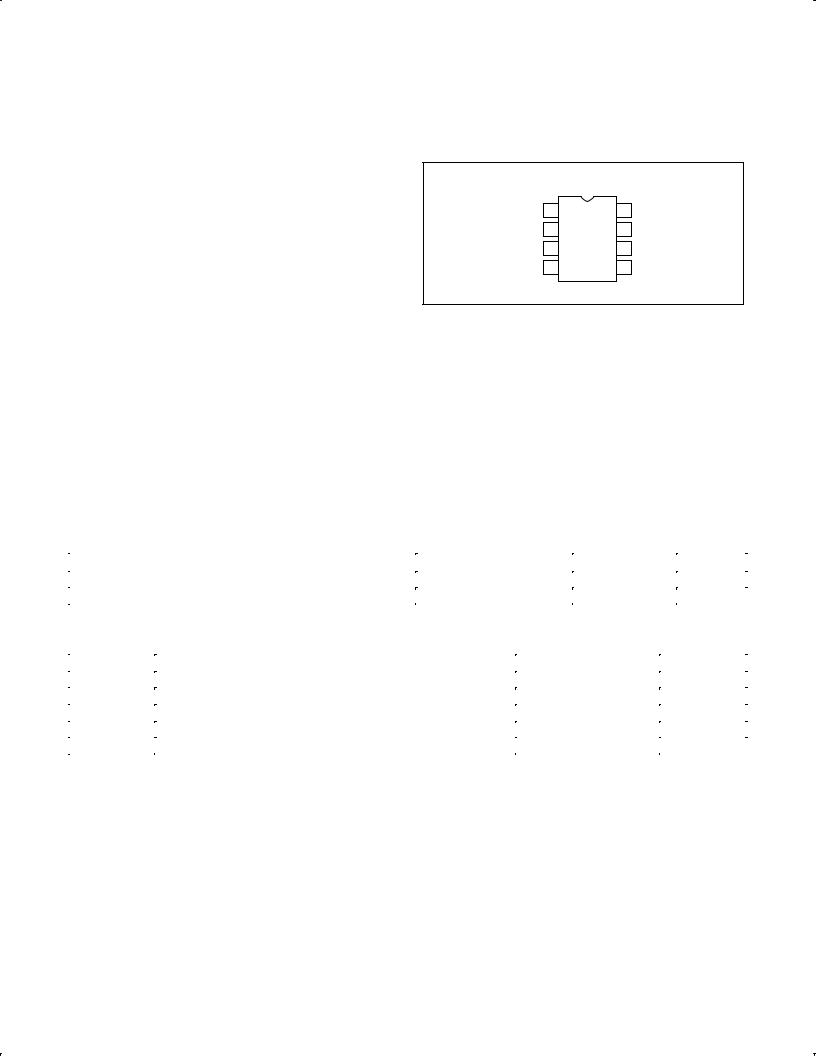
PIN CONFIGURATION
D and N Packages
INA |
1 |
8 |
VCC |
INB |
2 |
7 |
OSCE |
GND |
3 |
6 |
OSCB |
OUTA |
4 |
5 |
OUTB |
SR00068
Figure 1. Pin Configuration
APPLICATIONS
•Cellular radio mixer/oscillator
•Portable radio
•VHF transceivers
•RF data links
•HF/VHF frequency conversion
•Instrumentation frequency conversion
•Broadband LANs
ORDERING INFORMATION
DESCRIPTION |
TEMPERATURE RANGE |
ORDER CODE |
DWG # |
|
|
|
|
8-Pin Plastic Dual In-Line Plastic (DIP) |
-40 to +85°C |
SA602AN |
SOT97-1 |
|
|
|
|
8-Pin Plastic Small Outline (SO) package (Surface-mount) |
-40 to +85°C |
SA602AD |
SOT96-1 |
ABSOLUTE MAXIMUM RATINGS
SYMBOL |
|
PARAMETER |
RATING |
UNITS |
|
|
|
|
|
VCC |
Maximum operating voltage |
|
9 |
V |
TSTG |
Storage temperature range |
|
-65 to +150 |
°C |
TA |
Operating ambient temperature range SA602A |
-40 to +85 |
°C |
|
θJA |
Thermal impedance |
D package |
90 |
°C/W |
|
|
N package |
75 |
°C/W |
1997 Nov 07 |
2 |
853-1424 18662 |
Philips Semiconductors |
Product specification |
|
|
|
|
Double-balanced mixer and oscillator |
SA602A |
|
|
|
|
BLOCK DIAGRAM
8 |
7 |
6 |
5 |
VCC |
|
|
|
VOLTAGE |
|
OSCILLATOR |
|
REGULATOR |
|
|
|
|
|
GROUND |
|
1 |
2 |
3 |
4 |
SR00069
Figure 2. Block Diagram
AC/DC ELECTRICAL CHARACTERISTICS
VCC = +6V, |
TA = 25°C; unless otherwise stated. |
|
|
|
|
|
|
|
|
|
LIMITS |
|
|
|
|
|
|
|
|
|
SYMBOL |
PARAMETER |
TEST CONDITIONS |
|
SA602A |
|
UNITS |
|
|
|
|
|
|
|
|
|
|
MIN |
TYP |
MAX |
|
|
|
|
|
|
|
|
VCC |
Power supply voltage range |
|
4.5 |
|
8.0 |
V |
|
DC current drain |
|
|
2.4 |
2.8 |
mA |
|
|
|
|
|
|
|
fIN |
Input signal frequency |
|
|
500 |
|
MHz |
fOSC |
Oscillator frequency |
|
|
200 |
|
MHz |
|
Noise figure at 45MHz |
|
|
5.0 |
5.5 |
dB |
|
|
|
|
|
|
|
|
Third-order intercept point |
RFIN = -45dBm: f1 = 45.0MHz |
|
-13 |
-15 |
dBm |
|
|
f2 = 45.06MHz |
|
|
|
|
|
Conversion gain at 45MHz |
|
14 |
17 |
|
dB |
|
|
|
|
|
|
|
RIN |
RF input resistance |
|
1.5 |
|
|
kΩ |
CIN |
RF input capacitance |
|
|
3 |
3.5 |
pF |
|
Mixer output resistance |
(Pin 4 or 5) |
|
1.5 |
|
kΩ |
DESCRIPTION OF OPERATION
The SA602A is a Gilbert cell, an oscillator/buffer, and a temperature compensated bias network as shown in the equivalent circuit. The
Gilbert cell is a differential amplifier (Pins 1 and 2) which drives a balanced switching cell. The differential input stage provides gain and determines the noise figure and signal handling performance of the system.
The SA602A is designed for optimum low power performance. When used with the SA604 as a 45MHz cellular radio second IF and demodulator, the SA602A is capable of receiving -119dBm signals with a 12dB S/N ratio. Third-order intercept is typically -13dBm (that is approximately +5dBm output intercept because of the RF gain). The system designer must be cognizant of this large signal limitation. When designing LANs or other closed systems where transmission levels are high, and small-signal or signal-to-noise issues are not critical, the input to the SA602A should be appropriately scaled.
Besides excellent low power performance well into VHF, the
SA602A is designed to be flexible. The input, RF mixer output and oscillator ports can support a variety of configurations provided the designer understands certain constraints, which will be explained here.
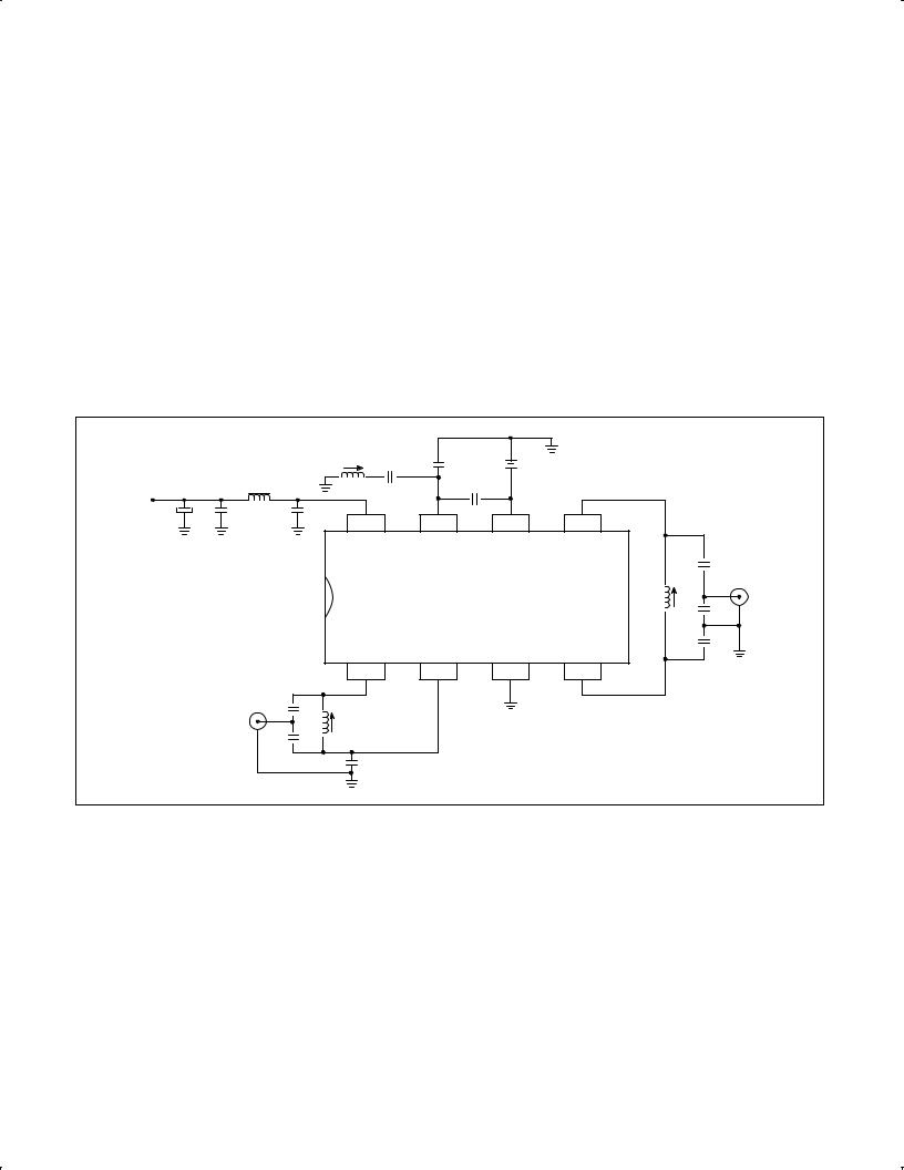
The RF inputs (Pins 1 and 2) are biased internally. They are symmetrical. The equivalent AC input impedance is approximately 1.5k || 3pF through 50MHz. Pins 1 and 2 can be used interchangeably, but they should not be DC biased externally.
Figure 5 shows three typical input configurations.
The mixer outputs (Pins 4 and 5) are also internally biased. Each output is connected to the internal positive supply by a 1.5kΩ resistor. This permits direct output termination yet allows for balanced output as well. Figure 6 shows three single ended output configurations and a balanced output.
1997 Nov 07 |
3 |
Philips Semiconductors |
Product specification |
|
|
|
|
Double-balanced mixer and oscillator |
SA602A |
|
|
|
|
The oscillator is capable of sustaining oscillation beyond 200MHz in crystal or tuned tank configurations. The upper limit of operation is determined by tank ªQº and required drive levels. The higher the
ªQº of the tank or the smaller the required drive, the higher the permissible oscillation frequency. If the required LO is beyond oscillation limits, or the system calls for an external LO, the external signal can be injected at Pin 6 through a DC blocking capacitor.
External LO should be at least 200mVP-P.
Figure 7 shows several proven oscillator circuits. Figure 7a is appropriate for cellular radio. As shown, an overtone mode of operation is utilized. Capacitor C3 and inductor L1 suppress oscillation at the crystal fundamental frequency. In the fundamental mode, the suppression network is omitted.
Figure 8 shows a Colpitts varactor tuned tank oscillator suitable for synthesizer-controlled applications. It is important to buffer the
output of this circuit to assure that switching spikes from the first counter or prescaler do not end up in the oscillator spectrum. The dual-gate MOSFET provides optimum isolation with low current.
The FET offers good isolation, simplicity, and low current, while the bipolar transistors provide the simple solution for non-critical applications. The resistive divider in the emitter-follower circuit should be chosen to provide the minimum input signal which will assure correct system operation.
When operated above 100MHz, the oscillator may not start if the Q of the tank is too low. A 22kΩ resistor from Pin 7 to ground will increase the DC bias current of the oscillator transistor. This improves the AC operating characteristic of the transistor and should help the oscillator to start. A 22kΩ resistor will not upset the other DC biasing internal to the device, but smaller resistance values should be avoided.
|
|
0.5 to 1.3μH |
|
22pF |
|
|
|
|
|
|
|
|
5.5μH |
|
|
|
34.545MHz THIRD OVERTONE CRYSTAL |
VCC |
|
1nF |
|
10pF |
|
6.8μF |
100nF |
8 |
7 |
6 |
5 |
|
10nF |
||||
|
|
|
|
|
150pF |
|
|
|
|
|
OUTPUT |
|
|
|
|
602A |
1.5 to |
|
|
|
|
44.2μH |
|
|
|
|
|
|
330pF |
|
|
|
|
|
120pF |
|
|
1 |
2 |
3 |
4 |
|
47pF |
|
|
|
|
|
INPUT |
0.209 to 0.283μH |
|
|
|
|
220pF |
|
|
|
|
|
|
100nF |
|
|
|
|
|
|
|
|
SR00070 |
Figure 3. Test Configuration
1997 Nov 07 |
4 |
 Loading...