


Philips NE5532AN, NE5532N, NE5532D8, NE5532D, NE5532NB Datasheet
...INTEGRATED CIRCUITS
NE/SA/SE5532/5532A
Internally-compensated dual low noise operational amplifier
Product specification |
1997 Sept 29 |
IC11 Data Handbook
m n r
Philips Semiconductors |
Product specification |
|
|
|
|
|
|
|
Internally-compensated dual low noise
NE/SA/SE5532/5532A
operational amplifier
DESCRIPTION |
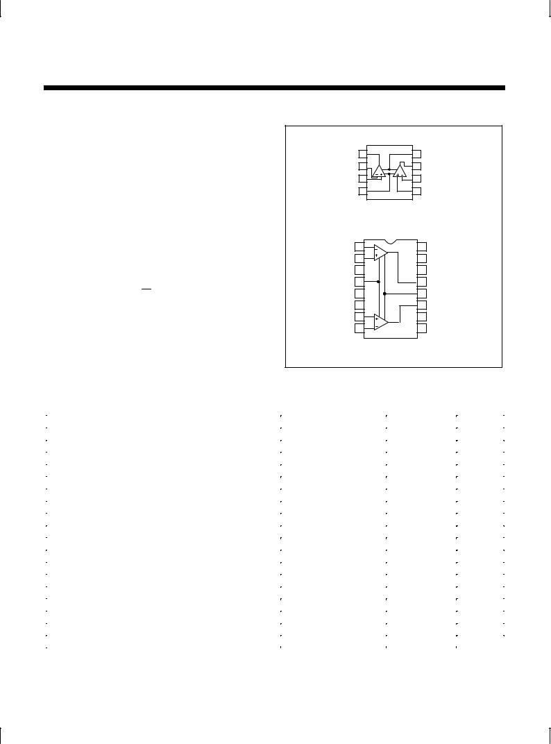
PIN CONFIGURATIONS |
The 5532 is a dual high-performance low noise operational amplifier. Compared to most of the standard operational amplifiers, such as the 1458, it shows better noise performance, improved output drive capability and considerably higher small-signal and power bandwidths.
This makes the device especially suitable for application in high-quality and professional audio equipment, instrumentation and control circuits, and telephone channel amplifiers. The op amp is internally compensated for gains equal to one. If very low noise is of prime importance, it is recommended that the 5532A version be used because it has guaranteed noise voltage specifications.
FEATURES
•Small-signal bandwidth: 10MHz
•Output drive capability: 600Ω, 10VRMS
•Input noise voltage: 5nV Hz (typical)
•DC voltage gain: 50000
•AC voltage gain: 2200 at 10kHz
•Power bandwidth: 140kHz
•Slew rate: 9V/μs
•Large supply voltage range: ±3 to ±20V
•Compensated for unity gain
FE, N, D8 Packages |
|
||
OUTPUT A |
1 |
8 |
V+ |
INVERTING INPUT A |
2 |
7 |
OUTPUT B |
|
A |
B |
|
NON-INVERTING INPUT A |
3 |
6 |
INVERTING INPUT B |
V- |
4 |
5 |
NON-INVERTING INPUT B |
TOP VIEW
|
|
D Package1 |
|
±INA |
1 |
16 |
NC |
+INA |
2 |
15 |
NC |
NC |
3 |
14 |
NC |
±VCC |
4 |
13 |
OUTA |
NC |
5 |
12 |
+VCC |
|
|
|
|
NC |
6 |
11 |
OUTB |
+INB |
7 |
10 |
NC |
|
|
|
|
±INB |
8 |
9 |
NC |
TOP VIEW
NOTE:
1. SOL and non-standard pinout. |
SL00332 |
|
Figure 1. Pin Configurations
ORDERING INFORMATION
DESCRIPTION |
TEMPERATURE RANGE |
ORDER CODE |
DWG # |
|
|
|
|
8-Pin Plastic Dual In-Line Package (DIP) |
0 to 70°C |
NE5532N |
SOT97-1 |
|
|
|
|
8-Pin Plastic Dual In-Line Package (DIP) |
±40°C to +85°C |
SA5532N |
SOT97-1 |
|
|
|
|
8-Pin Plastic Dual In-Line Package (DIP) |
±40°C to +85°C |
SA5532AN |
SOT97-1 |
|
|
|
|
8-Pin Ceramic Dual In-Line Package (CERDIP) |
0 to 70°C |
NE5532FE |
0580A |
|
|
|
|
8-Pin Plastic Dual In-Line Package (DIP) |
0 to 70°C |
NE5532AN |
SOT97-1 |
|
|
|
|
8-Pin Ceramic Dual In-Line Package (CERDIP) |
0 to 70°C |
NE5532AF |
0580A |
|
|
|
|
8-Pin Ceramic Dual In-Line Package (CERDIP) |
-55°C to +125°C |
SE5532FE |
0580A |
|
|
|
|
8-Pin Ceramic Dual In-Line Package (CERDIP) |
-55°C to +125°C |
SE5532AF |
0580A |
|
|
|
|
8-Pin Small Outline Package (SO) |
0 to 70°C |
NE5532AD8 |
SOT96-1 |
|
|
|
|
8-Pin Small Outline Package (SO) |
±40°C to 85°C |
SA5532D8 |
SOT96-1 |
|
|
|
|
8-Pin Small Outline Package (SO) |
±40°C to 85°C |
SA5532AD8 |
SOT96-1 |
|
|
|
|
8-Pin Small Outline Package (SO) |
-55°C to +125°C |
SE5532AD8 |
SOT96-1 |
|
|
|
|
8-Pin Small Outline Package (SO) |
0 to 70°C |
NE5532D8 |
SOT96-1 |
|
|
|
|
8-Pin Small Outline Package (SO) |
±40°C to 85°C |
SA5532D8 |
SOT96-1 |
|
|
|
|
8-Pin Small Outline Package (SO) |
±40°C to 85°C |
SA5532AD8 |
SOT96-1 |
|
|
|
|
8-Pin Small Outline Package (SO) |
-55°C to +125°C |
SE5532D8 |
SOT96-1 |
|
|
|
|
16-Pin Plastic Small Outline Large (SOL) Package |
0 to 70°C |
NE5532D |
SOT162-1 |
|
|
|
|
16-Pin Plastic Dual In-Line Package (DIP) |
-55°C to +125°C |
SE5532N |
SOT38-4 |
|
|
|
|
1997 Sept 29 |
2 |
853-0949 16639 |

Philips Semiconductors |
Product specification |
|
|
|
|
Internally-compensated dual low noise
NE/SA/SE5532/5532A
operational amplifier
EQUIVALENT SCHEMATIC (EACH AMPLIFIER)
+ |
_ |
SL00333 |
Figure 2. Equivalent Schematic (Each Amplifier)
ABSOLUTE MAXIMUM RATINGS
SYMBOL |
|
PARAMETER |
RATING |
UNIT |
|
|
|
|
|
VS |
Supply voltage |
±22 |
V |
|
VIN |
Input voltage |
±VSUPPLY |
V |
|
VDIFF |
Differential input voltage1 |
±0.5 |
V |
|
TA |
Operating temperature range |
|
°C |
|
|
SA5532/A |
±40 to +85 |
||
|
NE5532/A |
0 to 70 |
°C |
|
|
SE5532/A |
-55 to +125 |
°C |
|
|
|
|
|
|
TSTG |
Storage temperature |
-65 to +150 |
°C |
|
TJ |
Junction temperature |
150 |
°C |
|
PD |
Maximum power dissipation, |
|
|
|
|
T =25°C (still-air)2 |
|
|
|
|
A |
|
|
|
|
8 |
D8 package |
780 |
mW |
|
8 |
N package |
1200 |
mW |
|
8 |
FE package |
1000 |
mW |
|
16 |
D package |
1200 |
mW |
|
|
|
|
|
TSOLD |
Lead soldering temperature (10sec max) |
300 |
°C |
|
NOTES:
1.Diodes protect the inputs against over-voltage. Therefore, unless current-limiting resistors are used, large currents will flow if the differential input voltage exceeds 0.6V. Maximum current should be limited to ±10mA.
2.Thermal resistances of the above packages are as follows:
N package at 100°C/W
F package at 135°C/W
D package at 105°C/W
D8 package at 160°C/W
1997 Sept 29 |
3 |

Philips Semiconductors |
Product specification |
|
|
|
|
Internally-compensated dual low noise
NE/SA/SE5532/5532A
operational amplifier
DC ELECTRICAL CHARACTERISTICS
T =25°C V |
=±15V, unless otherwise specified. 1, 2, 3 |
|
|
|
|
|
|
|
|
||
A |
S |
|
|
|
|
|
|
|
|
|
|
SYMBOL |
|
PARAMETER |
TEST CONDITIONS |
SE/5532/5532A |
NE/SA/5532/5532A |
UNIT |
|||||
|
|
|
|
|
|
|
|||||
|
Min |
Typ |
Max |
Min |
Typ |
Max |
|||||
|
|
|
|
|
|
||||||
|
|
|
|
|
|
|
|
|
|
|
|
VOS |
|
|
Offset voltage |
|
|
0.5 |
2 |
|
0.5 |
4 |
mV |
|
|
|
|
Over temperature |
|
|
3 |
|
|
5 |
mV |
VOS/ |
T |
|
|
|
|
5 |
|
|
5 |
|
μV/°C |
IOS |
|
|
Offset current |
|
|
|
100 |
|
10 |
150 |
nA |
|
|
|
|
Over temperature |
|
|
200 |
|
|
200 |
nA |
IOS/ |
T |
|
|
|
|
200 |
|
|
200 |
|
pA/°C |
IB |
|
|
Input current |
|
|
200 |
400 |
|
200 |
800 |
nA |
|
|
|
|
Over temperature |
|
|
700 |
|
|
1000 |
nA |
IB/ T |
|
|
|
|
|
5 |
|
|
5 |
|
nA/°C |
|
|
|
|
|
|
8 |
10.5 |
|
8 |
16 |
mA |
ICC |
|
|
Supply current |
|
|
|
|
|
|
|
|
|
|
|
|
Over temperature |
|
|
13 |
|
|
|
mA |
|
|
|
|
|
|
|
|
|
|
|
|
VCM |
|
|
Common-mode input range |
|
±12 |
±13 |
|
±12 |
±13 |
|
V |
CMRR |
|
Common-mode rejection ratio |
|
80 |
100 |
|
70 |
100 |
|
dB |
|
|
|
|
|
|
|
|
|
|
|
|
|
PSRR |
|
|
Power supply rejection ratio |
|
|
10 |
50 |
|
10 |
100 |
μV/V |
|
|
|
|
|
|
|
|
|
|
|
|
|
|
|
|
RL≥ 2kΩ, VO=±10V |
50 |
100 |
|
25 |
100 |
|
V/mV |
AVOL |
|
|
Large-signal voltage gain |
Over temperature |
25 |
|
|
15 |
|
|
V/mV |
|
|
RL≥ 600Ω, VO=±10V |
40 |
50 |
|
15 |
50 |
|
V/mV |
||
|
|
|
|
|
|
||||||
|
|
|
|
Over temperature |
20 |
|
|
10 |
|
|
V/mV |
|
|
|
|
|
|
|
|
|
|
|
|
|
|
|
|
RL≥ 600Ω |
±12 |
±13 |
|
±12 |
±13 |
|
|
|
|
|
|
Over temperature |
±10 |
±12 |
|
±10 |
±12 |
|
|
VOUT |
|
|
Output swing |
RL≥ 600Ω, VS=±18V |
±15 |
±16 |
|
±15 |
±16 |
|
V |
|
|
Over temperature |
±12 |
±14 |
|
±12 |
±14 |
|
|||
|
|
|
|
|
|
|
|||||
|
|
|
|
RL≥ 2kΩ |
±13 |
±13.5 |
|
±13 |
±13.5 |
|
|
|
|
|
|
Over temperature |
±12 |
±12.5 |
|
±10 |
±12.5 |
|
|
|
|
|
|
|
|
|
|
|
|
|
|
RIN |
|
|
Input resistance |
|
30 |
300 |
|
30 |
300 |
|
kΩ |
ISC |
|
|
Output short circuit current |
|
10 |
38 |
60 |
10 |
38 |
60 |
mA |
NOTES:
1.Diodes protect the inputs against overvoltage. Therefore, unless current-limiting resistors are used, large currents will flow if the differential input voltage exceeds 0.6V. Maximum current should be limited to ±10mA.
2.For operation at elevated temperature, derate packages based on the package thermal resistance.
3.Output may be shorted to ground at VS=±15V, TA=25°C Temperature and/or supply voltages must be limited to ensure dissipation rating is not exceeded.
AC ELECTRICAL CHARACTERISTICS
TA=25°C VS=±15V, unless otherwise specified.
SYMBOL |
PARAMETER |
TEST CONDITIONS |
NE/SA/SE5532/5532A |
UNIT |
|||
|
|
|
|||||
Min |
Typ |
Max |
|||||
|
|
|
|
||||
|
|
|
|
|
|
|
|
ROUT |
Output resistance |
AV=30dB Closed-loop |
|
0.3 |
|
Ω |
|
f=10kHz, RL=600Ω |
|
|
|||||
|
|
|
|
|
|
||
|
|
Voltage-follower |
|
|
|
|
|
|
Overshoot |
VIN=100mVP-P |
|
10 |
|
% |
|
|
|
CL=100pF, RL=600Ω |
|
|
|
|
|
AV |
Gain |
f=10kHz |
|
2.2 |
|
V/mV |
|
GBW |
Gain bandwidth product |
CL=100pF, RL=600Ω |
|
10 |
|
MHz |
|
SR |
Slew rate |
|
|
9 |
|
V/μs |
|
|
|
|
|
|
|
|
|
|
|
VOUT=±10V |
|
140 |
|
kHz |
|
|
Power bandwidth |
VOUT=±14V, RL=600Ω, |
|
100 |
|
kHz |
|
|
|
VCC=±18V |
|
|
|
|
|
1997 Sept 29 |
4 |
 Loading...