


INTEGRATED CIRCUITS
74F543
Octal registered transceiver, non-inverting (3-State)
74F544
Octal registered transceiver, inverting (3-State)
Product specification |
1994 Dec 5 |
IC15 Data Handbook
Philips Semiconductors

Philips Semiconductors |
Product specification |
|
|
|
|
|
|
|
Octal registered transceivers |
74F543, 74F544 |
|
74F543 Octal registered transceiver, non-inverting (3-State) 74F544 Octal registered transceiver, inverting 93-State)
FEATURES
•Combines74F245 and 74F373 type functions in one chip
•8-bit octal transceiver with D-type latch
•74F543 Non-inverting 74F544 Inverting
•Back-to-back registers for storage
•Separate controls for data flow in each direction
•A outputs sink 20mA and source 3mA
•B outputs sink 64mA and source 15mA
•3-State outputs for bus-oriented applications
•74F543 available in SSOP Type II package
DESCRIPTION
The 74F543 and 74F544 Octal Registered Transceivers contain two sets of D-type latches for temporary storage of data flowing in either direction. Separate Latch Enable (LEAB, LEBA) and Output Enable (OEAB, OEBA) inputs are provided for each register to permit independent control of inputting and outputting in either direction of data flow. While the 74F543 has non-inverting data path, the 74F544 inverts data in both directions. The A outputs are guaranteed to sink
24mA, while the B outputs are rated for 64mA.
FUNCTIONAL DESCRIPTION
The 74F543 and 74F544 contain two sets of eight D-type latches, with separate input and controls for each set. For data flow from A to
B, for example, the A-to-B Enable (EAB) input must be Low in order to enter data from A0 - A7 or take data from B0 - B7, as indicated in the Function Table. With EAB Low, a Low signal on the A-to-B Latch Enable (LEAB) input makes the A-to-B latches transparent; a subsequent Low-to-High transition for the LEAB signal puts the
A latches in the storage mode and their outputs no longer change with the A inputs. With EAB and OEAB both Low, the 3-State
B output buffers are active and display the data present at the outputs of the A latches. Control of data flow from B to A is similar, but using the EBA, LEBA, and OEBA inputs.
|
TYPICAL |
TYPICAL |
TYPE |
PROPAGATION |
SUPPLY CURRENT |
|
DELAY |
(TOTAL) |
|
|
|
74F543 |
6.0ns |
80mA |
|
|
|
74F544 |
6.5ns |
95mA |
|
|
|
ORDERING INFORMATION
|
COMMERCIAL RANGE |
DRAWING |
|
DESCRIPTION |
VCC = 5V ±10%, |
||
NUMBER |
|||
|
TA = 0°C to +70°C |
|
|
24-pin plastic skinny DIP (300mil) |
N74F543N, |
SOT222±1 |
|
N74F544N |
|||
|
|
||
|
|
|
|
24-pin plastic SOL |
N74F543D, |
SOT137-1 |
|
N74F544D |
|||
|
|
||
|
|
|
|
24-pin plastic SSOP Type II |
74F543DB |
SOT340-1 |
|
|
|
|
INPUT AND OUTPUT LOADING AND FAN-OUT TABLE
|
PINS |
|
|
DESCRIPTION |
|
74F(U.L.) |
LOAD VALUE |
||||||||||
|
|
|
|
HIGH/LOW |
HIGH/LOW |
||||||||||||
|
|
|
|
|
|
|
|
|
|
|
|
|
|
|
|
||
|
|
|
|
|
|
|
|
|
|
|
|
|
|
|
|
|
|
|
|
|
A0 - A7 |
Port A, 3-State inputs |
|
3.5/1.0 |
70μA/0.6mA |
||||||||||
|
|
|
|
|
|
|
|
|
|
|
|
|
|
|
|
|
|
|
|
|
B0 - B7 |
Port B, 3-State inputs |
|
3.5/1.0 |
70μA/0.6mA |
||||||||||
|
|
|
|
|
|
|
|
|
|
|
|
|
|
|
|
|
|
|
|
|
|
|
|
|
|
|
|
|
|
A-to-B Output Enable input (Active Low) |
|
1.0/1.0 |
20μA/0.6mA |
||
|
|
|
OEAB |
|
|||||||||||||
|
|
|
|
|
|
|
|
|
|
|
|
B-to-A Output Enable input (Active Low) |
|
1.0/1.0 |
20μA/0.6mA |
||
74F543 |
|
|
OEBA |
|
|||||||||||||
74F544 |
|
|
|
|
|
|
|
|
|
|
A-to-B Enable input (Active Low) |
|
1.0/2.0 |
20μA/1.2mA |
|||
|
|
EAB |
|
||||||||||||||
|
|
|
|
|
|
|
|
|
|
|
B-to-A Enable input (Active Low) |
|
1.0/2.0 |
20μA/1.2mA |
|||
|
|
|
EBA |
|
|||||||||||||
|
|
|
|
|
|
|
|
|
|
|
A-to-B Latch Enable input (Active Low) |
|
1.0/1.0 |
20μA/0.6mA |
|||
|
|
|
LEAB |
|
|||||||||||||
|
|
|
|
|
|
|
|
|
|
|
B-to-A Latch Enable input (Active Low) |
|
1.0/1.0 |
20μA/0.6mA |
|||
|
|
|
LEBA |
|
|||||||||||||
74F543 |
|
|
A0 - A7 |
Port A, 3-State outputs |
|
150/40 |
3.0mA/24mA |
||||||||||
|
|
|
|
|
|
|
|
|
|
|
|
|
|
|
|
|
|
|
|
B0 - B7 |
Port B, 3-State outputs |
|
750/106.7 |
15mA/64mA |
|||||||||||
|
|
|
|
||||||||||||||
|
|
|
|
|
|
|
|
|
|
|
|
|
|||||
|
|
|
|
|
|
|
Port |
|
|
|
150/40 |
3.0mA/24mA |
|||||
74F544 |
|
|
A0 - A7 |
A, 3-State outputs |
|
||||||||||||
|
|
|
|
|
|
|
|
|
|
|
Port |
|
|
|
750/106.7 |
15mA/64mA |
|
|
|
|
B0 - B7 |
B, 3-State outputs |
|
||||||||||||
NOTE: One (1.0) FAST Unit Load is defined as: 20μA in the High State and 0.6mA in the Low state. |
|
|
|||||||||||||||
1994 Dec 5 |
|
|
|
|
|
|
|
|
|
|
|
2 |
|
|
853-0874 14379 |
||

Philips Semiconductors |
Product specification |
|
|
|
|
Octal registered transceivers |
74F543, 74F544 |
|
|
|
|
PIN CONFIGURATION ± 74F543 |
|
LOGIC SYMBOL ± 74F543 |
|
|
|
|
|
|||||||
LEBA |
1 |
|
24 |
VCC |
|
3 |
4 |
5 |
6 |
7 |
8 |
9 |
10 |
|
|
|
|
|
|
|
|
|
|
|
|
||||
OEBA |
2 |
|
23 |
EBA |
|
|
|
|
|
|
|
|
|
|
A0 |
3 |
|
22 |
B0 |
|
|
|
|
|
|
|
|
|
|
|
4 |
|
21 |
|
|
A0 A1 A2 A3 A4 A5 A6 A7 |
|
|||||||
A1 |
|
B1 |
|
|
|
|
|
|
|
|
|
|
||
A2 |
5 |
|
20 |
B2 |
11 |
EAB |
|
|
|
|
|
|
|
|
|
|
|
|
|
|
|
|
|
|
13 |
||||
|
6 |
|
19 |
|
23 |
EBA |
|
|
|
|
|
|
OEAB |
|
A3 |
|
B3 |
14 |
LEAB |
|
|
|
|
|
|
OEBA |
2 |
||
|
|
|
|
|
|
|
|
|
|
|
||||
A4 |
7 |
|
18 |
B4 |
1 |
LEBA |
|
|
|
|
|
|
|
|
A5 |
8 |
|
17 |
B5 |
|
|
|
|
|
|
|
|
|
|
A6 |
9 |
|
16 |
B6 |
|
B0 B1 B2 B3 B4 B5 B6 B7 |
|
|||||||
|
|
|
|
|
|
|
|
|
|
|
||||
A7 |
10 |
|
15 |
B7 |
|
|
|
|
|
|
|
|
|
|
EAB |
11 |
|
14 |
LEAB |
|
22 |
21 |
20 |
19 |
18 |
17 |
16 |
15 |
|
|
|
|
|
|
|
|
||||||||
GND |
12 |
|
13 |
OEAB |
VCC = Pin 24 |
|
|
|
|
|
|
|
|
|
|
|
|
|
|
GND = Pin 12 |
|
|
|
|
|
|
|
|
|
|
|
|
SF00237 |
|
|
|
|
|
|
|
|
|
SF00238 |
|
LOGIC SYMBOL (IEEE/IEC) ± 74F543 |
|
|
|
|
|
|
|
|
|
|
||||
2 |
|
IEN3 |
|
|
|
|
|
|
|
|
|
|
|
|
|
|
|
|
|
|
|
|
|
|
|
|
|
|
|
23 |
|
G1 |
|
|
|
|
|
|
|
|
|
|
|
|
1 |
|
1C5 |
|
|
|
|
|
|
|
|
|
|
|
|
13 |
|
2EN4 |
|
|
|
|
|
|
|
|
|
|
|
|
11 |
|
G2 |
|
|
|
|
|
|
|
|
|
|
|
|
14 |
|
2C6 |
|
|
|
|
|
|
|
|
|
|
|
|
3 |
|
3 |
5D |
22 |
|
|
|
|
|
|
|
|
|
|
|
|
|
|
|
|
|
|
|
|
|
|
|
||
4 |
|
6D |
4 |
21 |
|
|
|
|
|
|
|
|
|
|
|
|
|
|
|
|
|
|
|
|
|
|
|
||
5 |
|
|
|
20 |
|
|
|
|
|
|
|
|
|
|
6 |
|
|
|
19 |
|
|
|
|
|
|
|
|
|
|
7 |
|
|
|
18 |
|
|
|
|
|
|
|
|
|
|
8 |
|
|
|
17 |
|
|
|
|
|
|
|
|
|
|
9 |
|
|
|
16 |
|
|
|
|
|
|
|
|
|
|
10 |
|
|
|
15 |
|
|
|
|
|
|
|
|
|
|
|
|
|
|
SF00239 |
|
|
|
|
|
|
|
|
|
|
1994 Dec 5 |
3 |

Philips Semiconductors |
Product specification |
|
|
|
|
Octal registered transceivers |
74F543, 74F544 |
|
|
|
|
PIN CONFIGURATION ± 74F544 |
|
LOGIC SYMBOL ± 74F544 |
|
|
|
|
|
||||||
LEBA |
1 |
24 |
VCC |
|
3 |
4 |
5 |
6 |
7 |
8 |
9 |
10 |
|
|
|
|
|
|
|
|
|
|
|
||||
OEBA |
2 |
23 |
EBA |
|
|
|
|
|
|
|
|
|
|
A0 |
3 |
22 |
B0 |
|
|
|
|
|
|
|
|
|
|
A1 |
4 |
21 |
B1 |
|
A0 A1 A2 A3 A4 A5 A6 A7 |
|
|||||||
|
|
|
|
|
|
|
|
|
|
||||
A2 |
5 |
20 |
B2 |
11 |
EAB |
|
|
|
|
|
|
|
|
|
|
|
|
|
|
|
|
|
13 |
||||
A3 |
6 |
19 |
B3 |
23 |
EBA |
|
|
|
|
|
|
OEAB |
|
14 |
LEAB |
|
|
|
|
|
|
OEBA |
2 |
||||
|
|
|
|
|
|
|
|
|
|
||||
A4 |
7 |
18 |
B4 |
1 |
LEBA |
|
|
|
|
|
|
|
|
A5 |
8 |
17 |
B5 |
|
|
|
|
|
|
|
|
|
|
A6 |
9 |
16 |
B6 |
|
B0 B1 B2 B3 B4 B5 B6 B7 |
|
|||||||
|
|
|
|
|
|
|
|
|
|
||||
A7 |
10 |
15 |
B7 |
|
|
|
|
|
|
|
|
|
|
EAB |
11 |
14 |
LEAB |
|
|
|
|
|
|
|
|
|
|
GND |
12 |
13 |
OEAB |
VCC = Pin 24 |
22 |
21 |
20 |
19 |
18 |
17 |
16 |
15 |
|
|
|
|
|
|
|
|
|
|
|||||
|
|
|
|
GND = Pin 12 |
|
|
|
|
|
|
|
|
|
|
|
SF00240 |
|
|
|
|
|
|
|
|
SF00242 |
||
LOGIC SYMBOL (IEEE/IEC) ± 74F544
2 |
IEN3 |
|
|
23 |
G1 |
|
|
1 |
1C5 |
|
|
13 |
2EN4 |
|
|
11 |
G2 |
|
|
14 |
2C6 |
|
|
3 |
3 |
5D |
22 |
|
|
||
4 |
6D |
4 |
21 |
|
|
||
5 |
|
|
20 |
6 |
|
|
19 |
7 |
|
|
18 |
8 |
|
|
17 |
9 |
|
|
16 |
10 |
|
|
15 |
|
|
|
|
|
|
|
SF00241 |
FUNCTION TABLE for 74F543 and 74F544
|
|
|
|
|
|
INPUTS |
|
|
OUTPUTS |
STATUS |
||||||||||
|
|
|
|
|
|
|
|
|
|
|
|
|
|
|
|
|
|
|
||
|
|
|
|
|
|
|
|
|
|
|
|
DATA |
74F543 |
74F544 |
|
|||||
OEXX |
EXX |
LEXX |
|
|||||||||||||||||
|
|
H |
|
|
|
X |
|
X |
|
X |
Z |
|
Z |
Disabled |
||||||
|
|
|
|
|
|
|
|
|
|
|
|
|
|
|
|
|
|
|
||
|
|
X |
|
|
|
H |
|
X |
|
X |
Z |
|
Z |
Disabled |
||||||
|
|
|
|
|
|
|
|
|
|
|
|
|
|
|
|
|
|
|
||
|
|
L |
|
|
|
↑ |
|
L |
|
h |
Z |
|
Z |
Disable + |
||||||
|
|
L |
|
|
|
↑ |
|
L |
|
l |
Z |
|
Z |
Latch |
||||||
|
|
L |
|
|
|
L |
|
↑ |
|
h |
H |
|
L |
Latch + |
||||||
|
|
L |
|
|
|
L |
|
↑ |
|
l |
L |
|
H |
Display |
||||||
|
|
|
|
|
|
|
|
|
|
|
|
|
|
|
|
|
|
|
||
|
|
L |
|
|
|
L |
|
L |
|
H |
H |
|
L |
Transparent |
||||||
|
|
L |
|
|
|
L |
|
L |
|
L |
L |
|
H |
|||||||
|
|
|
|
|
|
|
|
|
||||||||||||
|
|
|
|
|
|
|
|
|
|
|
|
|
|
|
|
|
|
|
||
|
|
L |
|
|
|
L |
|
H |
|
X |
NC |
|
NC |
Hold |
||||||
H |
= |
High voltage level |
|
|
|
|
|
|
|
|
|
|||||||||
L |
= |
Low voltage level |
|
|
|
|
|
|
|
|
|
|||||||||
h |
= |
High state must be present one setup time before the |
||||||||||||||||||
|
|
|
Low-to-High transition of |
LEXX |
or |
EXX |
(XX=AB or BA) |
|||||||||||||
l |
= |
Low state must be present one setup time before the |
||||||||||||||||||
↑ |
|
Low-to-High transition of |
LEXX |
or |
EXX |
(XX=AB or BA) |
||||||||||||||
= |
Low-to-High transition of |
LEXX |
or |
EXX |
XX = AB or BA |
|||||||||||||||
X |
= |
Don't care |
|
|
|
|
|
|
|
|
|
|||||||||
NC = |
No change |
|
|
|
|
|
|
|
|
|
||||||||||
Z |
= |
High impedance ªoffº state |
|
|
|
|||||||||||||||
1994 Dec 5 |
4 |
Philips Semiconductors |
Product specification |
|
|
|
|
Octal registered transceivers |
74F543, 74F544 |
|
|
|
|
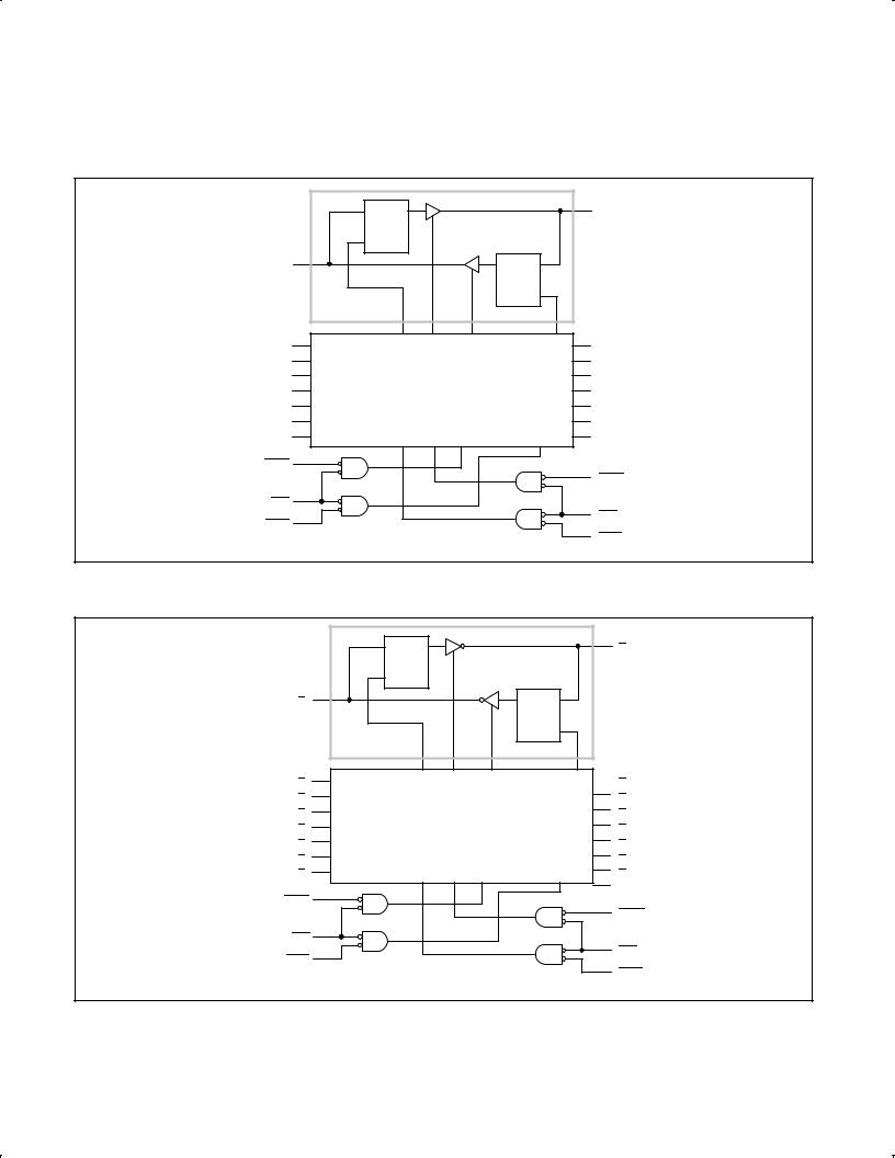
LOGIC DIAGRAM FOR 74F543
|
|
|
D |
Q |
DETAIL A |
22 |
B0 |
|
|
|
|
|
|
||||
|
|
|
LE |
|
|
|
|
|
|
A0 |
3 |
|
|
Q |
D |
|
|
|
|
|
|
|
LE |
|
|
|
|
A1 |
4 |
|
|
|
21 |
B1 |
|
|
A2 |
5 |
|
|
|
20 |
B2 |
|
|
A3 |
6 |
|
|
|
19 |
B3 |
|
|
A4 |
7 |
|
|
DETAIL A X 7 |
18 |
B4 |
|
|
A5 |
8 |
|
|
|
17 |
B5 |
|
|
A6 |
9 |
|
|
|
16 |
B6 |
|
|
A7 |
10 |
|
|
|
15 |
B7 |
|
|
OEBA |
2 |
|
|
|
|
|
|
|
|
|
|
|
|
|
|
|
|
|
|
|
|
|
13 |
OEAB |
|
|
EBA |
23 |
|
|
|
|
|
|
|
|
|
|
|
11 |
|
|
|
|
|
1 |
|
|
|
EAB |
|
|
|
LEBA |
|
|
|
|
|
||
|
|
|
|
|
|
|
||
VCC = Pin 24 |
|
|
|
|
14 |
|
|
|
|
|
|
|
|
LEAB |
|||
GND = Pin 12 |
|
|
|
|
|
|
||
|
|
|
|
|
|
|
|
|
|
|
|
|
|
|
SF00243 |
|
|
LOGIC DIAGRAM FOR 74F544 |
|
|
|
|
|
|
|
|
|
|
|
|
D |
DETAIL A |
22 |
B0 |
|
|
|
|
|
Q |
|
|
||
|
|
|
|
LE |
|
|
|
|
|
|
A0 |
3 |
|
Q |
D |
|
|
|
|
|
|
|
|
LE |
|
|
|
|
A1 |
4 |
|
|
|
21 |
B1 |
|
|
A2 |
5 |
|
|
|
20 |
B2 |
|
|
A3 |
6 |
|
|
|
19 |
B3 |
|
|
A4 |
7 |
|
DETAIL A X 7 |
|
18 |
B4 |
|
|
A5 |
8 |
|
|
|
17 |
B5 |
|
|
9 |
|
|
|
16 |
||
|
|
A6 |
|
|
|
B6 |
||
|
|
10 |
|
|
|
15 |
||
|
|
A7 |
|
|
|
B7 |
||
|
|
|
|
|
|
|
||
|
OEBA |
2 |
|
|
|
|
|
|
|
|
|
|
|
13 |
|
||
|
|
|
|
|
|
|
OEAB |
|
|
|
|
|
|
|
|
|
|
|
|
EBA |
23 |
|
|
|
|
|
|
|
|
|
|
|
11 |
|
|
|
|
|
1 |
|
|
|
EAB |
|
VCC = Pin 24 |
LEBA |
|
|
|
|
|||
|
|
|
|
|
||||
|
|
|
|
14 |
|
|||
GND = Pin 12 |
|
|
|
|
|
|
LEAB |
|
|
|
|
|
|
|
|
|
|
|
|
|
|
|
|
|
SF00244 |
|
1994 Dec 5 |
|
|
|
|
5 |
|
|
|
 Loading...