


Philips N74ALS241A-1D, N74ALS241A-1DB, N74ALS241A-1N, N74ALS241AD, N74ALS241ADB Datasheet
...
INTEGRATED CIRCUITS
74ALS241A/74ALS241A±1
Octal buffer (3±state)
Product specification |
1991 Feb 08 |
IC05 Data Handbook |
|
m n r
Philips Semiconductors |
Product specification |
|
|
|
|
|
|
|
Octal buffer (3-State) |
74ALS241A/74ALS241A-1 |
|
|
|
|
|
|
|
FEATURES
•Octal bus interface
•3-State buffer outputs sink 24mA and source 15mA
•The -1 version sinks 48 mA
DESCRIPTION
The 74ALS241A is an octal buffer that is ideal for driving bus lines or buffer memory address registers. The outputs are all capable of sinking 24mA and sourcing up to 15mA, producing very good capacitive drive characteristics. The device features two output enables, OEa and OEb, each controlling four of the 3-State outputs.
The 74ALS241A-1 sinks 48mA IOL if the VCC is limited to 5.0V ±0.25V.
|
TYPICAL |
TYPICAL |
TYPE |
PROPAGATION |
SUPPLY CURRENT |
|
DELAY |
(TOTAL) |
|
|
|
74ALS241A |
4.5ns |
18mA |
|
|
|
74ALS241A-1 |
4.5ns |
18mA |
|
|
|
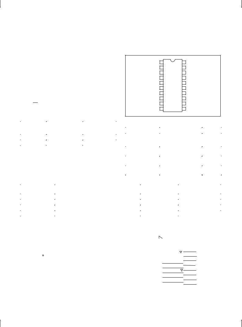
PIN CONFIGURATION
|
|
|
20 |
VCC |
OEa |
1 |
|||
Ia0 |
2 |
19 |
OEb |
|
Yb0 |
3 |
18 |
Ya0 |
|
Ia1 |
4 |
17 |
Ib0 |
|
Yb1 |
5 |
16 |
Ya1 |
|
Ia2 |
6 |
15 |
Ib1 |
|
Yb2 |
7 |
14 |
Ya2 |
|
Ia3 |
8 |
13 |
Ib2 |
|
Yb3 |
9 |
12 |
Ya3 |
|
GND |
10 |
11 |
Ib3 |
|
SF00324
ORDERING INFORMATION
|
ORDER CODE |
|
|
|
|
DRAWING |
|
|
COMMERCIAL RANGE |
||
|
NUMBER |
||
DESCRIPTION |
VCC = 5V ±10%, |
||
|
Tamb = 0°C to +70°C |
|
|
20-pin plastic DIP |
74ALS241AN, |
SOT146-1 |
|
74ALS241A-1N |
|||
|
|
||
|
|
|
|
20-pin plastic SOL |
74ALS241AD, |
SOT163-1 |
|
74ALS241A-1D |
|||
|
|
||
|
|
|
|
20-pin plastic SSOP |
74ALS241ADB, |
SOT339-1 |
|
Type II |
74ALS241A-1DB |
||
|
|||
|
|
|
INPUT AND OUTPUT LOADING AND FAN-OUT TABLE
|
PINS |
|
|
|
|
|
|
|
|
|
|
|
|
|
|
DESCRIPTION |
|
|
|
74ALS (U.L.) |
|
|
|
LOAD VALUE |
|||||||||||
|
|
|
|
|
|
|
|
|
|
|
|
|
|
|
|
|
|
|
HIGH/LOW |
|
|
|
HIGH/LOW |
||||||||||||
|
|
|
|
|
|
|
|
|
|
|
|
|
|
|
|
|
|
|
|
|
|
|
|
|
|
|
|
|
|
|
|||||
|
|
|
|
|
|
|
|
|
|
|
|
|
|
|
|
|
|
|
|
|
|
|
|
|
|
|
|
|
|
|
|
|
|
||
|
Ian, Ibn |
|
|
|
|
Data inputs |
|
|
|
|
|
|
|
|
|
|
|
|
1.0/1.0 |
|
|
|
|
20μA/0.1mA |
|||||||||||
|
|
|
|
|
|
|
|
|
|
|
|
|
|
|
|
|
|
|
|
|
|
|
|
|
|
|
|
|
|
||||||
|
|
|
|
|
|
|
|
|
|
|
Output Enable inputs (active-Low) |
|
|
|
|
|
1.0/1.0 |
|
|
|
|
20μA/0.1mA |
|||||||||||||
|
OEa, OEb |
|
|
|
|
|
|
|
|
|
|
|
|
||||||||||||||||||||||
|
|
|
|
|
|
|
|
|
|
|
|
|
|
|
|
|
|
|
|
|
|
|
|
|
|
|
|
|
|
||||||
|
Yan, Ybn |
|
|
|
|
Data outputs |
|
|
|
|
|
|
|
|
|
|
750/240 |
|
|
|
|
15mA/24mA |
|||||||||||||
|
|
|
|
|
|
|
|
|
|
|
|
|
|
|
|
|
|
|
|
|
|
|
|
|
|
|
|
||||||||
|
Yan, Ybn |
|
|
|
|
Data outputs (-1 version) |
|
|
|
|
|
750/480 |
|
|
|
|
15mA/48mA |
||||||||||||||||||
|
|
|
|
|
|
|
|
|
|
|
|
|
|
|
|
|
|
|
|
|
|
|
|
|
|
|
|
||||||||
NOTE: One (1.0) ALS unit load is defined as: 20μA in the High state and 0.1mA in the Low state. |
|
|
|
|
|||||||||||||||||||||||||||||||
LOGIC SYMBOL |
|
|
|
|
|
|
|
|
|
|
|
|
|
|
|
|
IEC/IEEE SYMBOL |
|
|
|
|
||||||||||||||
|
|
|
|
|
|
|
|
|
|
|
|
|
|
|
|
|
|
|
|
|
|
|
|
|
|
|
|
|
|
|
|
|
|
|
|
|
|
|
|
|
|
|
2 |
4 |
6 |
8 |
17 |
15 |
13 |
11 |
|
|
|
1 |
|
|
|
|
|
|
|
||||||||||
|
|
|
|
|
|
|
|
|
|
EN1 |
|
|
|
|
|||||||||||||||||||||
|
|
|
|
|
|
|
|
|
19 |
|
|
|
|
|
|||||||||||||||||||||
|
|
|
|
|
|
|
|
|
|
|
|
|
|
|
|
|
|
|
|
|
|
|
|
|
|
EN2 |
|
|
|
|
|||||
|
|
|
|
|
|
|
|
|
|
|
|
|
|
|
|
|
|
|
|
|
|
|
|
|
|
|
|
|
|
|
|
|
|
||
|
|
|
|
|
|
|
|
|
|
|
|
|
|
|
|
|
|
|
|
|
|
|
|
|
|
|
|
|
|
|
|
|
|
|
|
|
|
|
|
|
|
|
Ia0 |
Ia1 |
Ia2 |
Ia3 |
Ib0 |
Ib1 |
Ib2 |
Ib3 |
|
|
|
2 |
|
|
|
|
|
|
18 |
||||||||||
|
|
|
|
|
|
|
|
|
|
|
|
|
|
|
|
|
|
|
|
|
|
|
|
|
|
2D |
1 |
|
|||||||
1 |
|
|
|
|
OEa |
|
|
|
|
|
|
|
|
|
|
|
|
|
|
|
|
4 |
|
|
16 |
||||||||||
|
|
|
|
|
|
|
|
|
|
|
|
|
|
|
|
|
|
|
|
|
|
|
|
|
|
||||||||||
|
|
|
|
|
|
|
|
|
|
|
|
|
|
|
|
|
|
|
|
|
|
|
|
|
|||||||||||
|
|
|
|
|
|
|
|
|
|
|
|
|
|
|
|
|
|
|
|
|
|
|
|
|
|
|
|
|
|
14 |
|||||
19 |
|
|
|
|
OEb |
|
|
|
|
|
|
|
|
|
|
|
|
|
|
|
|
6 |
|
|
|
|
|
|
|||||||
|
|
|
|
|
|
|
|
|
|
|
|
|
|
|
|
|
|
|
|
|
|
|
|
|
|||||||||||
|
|
|
|
|
|
|
|
|
|
|
|
|
|
|
|
|
|
|
|
|
|
|
|
|
|
|
|
|
|
12 |
|||||
|
|
|
|
|
|
|
|
|
|
|
|
|
|
|
|
|
|
|
|
|
8 |
|
|
|
|
|
|
||||||||
|
|
|
|
|
|
|
|
|
|
|
|
|
|
|
|
|
|
|
|
|
|
|
|
|
|
|
|
|
|
|
|||||
|
|
|
|
|
|
|
Ya0 |
Ya1 Ya2 |
Ya3 Yb0 |
Yb1 Yb2 |
Yb3 |
|
|
|
17 |
|
|
|
2 |
|
3 |
||||||||||||||
|
|
|
|
|
|
|
|
|
|
|
|
|
|
|
|
|
|
|
|
|
|
|
|
|
|
15 |
|
|
|
|
|
|
5 |
||
|
|
|
|
|
|
|
18 |
16 |
14 |
12 |
3 |
5 |
7 |
9 |
|
|
|
13 |
|
|
|
|
|
|
7 |
||||||||||
VCC = Pin 20 |
|
|
|
|
|
|
|
|
|
|
|
|
|
|
|
|
|
|
11 |
|
|
|
|
|
|
9 |
|||||||||
|
|
|
|
|
|
|
|
|
|
|
|
|
|
|
|
|
|
|
|
|
|
|
|
|
|
|
|
|
|||||||
GND = Pin 10 |
|
|
|
|
|
|
|
|
|
|
|
|
|
|
|
|
SF00325 |
|
|
|
|
|
|
|
|
|
|
|
SF00326 |
||||||
|
|
|
|
|
|
|
|
|
|
|
|
|
|
|
|
|
|
|
|
|
|
|
|
|
|
|
|||||||||
|
|
|
|
|
|
|
|
|
|
|
|
|
|
|
|
|
|
|
|
|
|
|
|
|
|
|
|
|
|
|
|
|
|
||
|
|
|
|
|
|
|
|
|
|
|
|
|
|
|
|
|
|
|
|
|
|
|
|
|
|
|
|
|
|
|
|
|
|
|
|
1991 Feb 08 |
2 |
853±1276 01670 |

Philips Semiconductors |
Product specification |
|
|
|
|
Octal buffer (3-State) |
74ALS241A/74ALS241A-1 |
|
|
|
|
LOGIC DIAGRAM
Ia0 |
2 |
18 |
Ya0 |
Ib0 |
17 |
3 |
Yb0 |
|
|
|
|
||||
Ia1 |
4 |
16 |
Ya1 |
Ib1 |
15 |
5 |
Yb1 |
|
|
|
|
||||
Ia2 |
6 |
14 |
Ya2 |
Ib2 |
13 |
7 |
Yb2 |
|
|
|
|
||||
Ia3 8 |
12 |
Ya3 |
Ib3 |
11 |
9 |
Yb3 |
|
OEa |
1 |
|
|
OEb |
10 |
|
|
|
|
|
|
|
|
||
VCC = Pin 20
GND = Pin 10
SF00327
FUNCTION TABLE
|
|
|
|
INPUTS |
|
OUTPUTS |
|||||
|
|
|
|
|
|
|
|
|
|
|
|
|
|
|
|
Ia |
|
|
|
|
Ib |
Ya |
Yb |
|
OEa |
OEb |
|
||||||||
|
|
|
|
|
|
|
|
|
|
|
|
|
|
L |
|
L |
|
H |
|
L |
L |
L |
|
|
|
|
|
|
|
|
|
|
|
|
|
|
|
L |
|
H |
|
H |
|
H |
H |
H |
|
|
|
|
|
|
|
|
|
|
|
|
|
|
|
H |
|
X |
|
L |
|
X |
Z |
Z |
|
|
|
|
|
|
|
|
|
|
|
|
|
H |
= |
High voltage level |
|
|
|
|
|
|
|||
L |
= |
Low voltage level |
|
|
|
|
|
|
|||
X |
= |
Don't care |
|
|
|
|
|
|
|||
Z |
= |
High impedance ªoffº state |
|
|
|
||||||
ABSOLUTE MAXIMUM RATINGS
(Operation beyond the limit set forth in this table may impair the useful life of the device. Unless otherwise noted these limits are over the operating free air temperature range.)
SYMBOL |
PARAMETER |
RATING |
UNIT |
||
|
|
|
|
|
|
VCC |
Supply voltage |
±0.5 to +7.0 |
V |
||
VIN |
Input voltage |
±0.5 to +7.0 |
V |
||
IIN |
Input current |
±30 to +5 |
mA |
||
VOUT |
Voltage applied to output in High output state |
±0.5 to VCC |
V |
||
IOUT |
Current applied to output in Low output state |
All versions |
48 |
mA |
|
|
|
|
|||
-1 version |
96 |
mA |
|||
|
|
||||
|
|
|
|
|
|
Tamb |
Operating free-air temperature range |
0 to +70 |
°C |
||
Tstg |
Storage temperature range |
±65 to +150 |
°C |
||
RECOMMENDED OPERATING CONDITIONS
SYMBOL |
PARAMETER |
|
|
LIMITS |
|
UNIT |
|
|
MIN |
NOM |
MAX |
||
|
|
|
|
|||
|
|
|
|
|
|
|
VCC |
Supply voltage |
|
4.5 |
5.0 |
5.5 |
V |
VIH |
High-level input voltage |
|
2.0 |
|
|
V |
VIL |
Low-level input voltage |
|
|
|
0.8 |
V |
IIK |
Input clamp current |
|
|
|
±18 |
mA |
IOH |
High-level output current |
|
|
|
±15 |
mA |
IOL |
Low-level output current |
All versions |
|
|
24 |
mA |
|
|
|
|
|
||
-1 version |
|
|
48 1 |
mA |
||
|
|
|
|
|||
Tamb |
Operating free-air temperature range |
|
0 |
|
+70 |
°C |
NOTE:
1. The 48mA limit applies only under the condition of VCC = 5.0V ±5%.
1991 Feb 08 |
3 |
 Loading...