


DCR-TRV255E
Table of contents
 Loading...
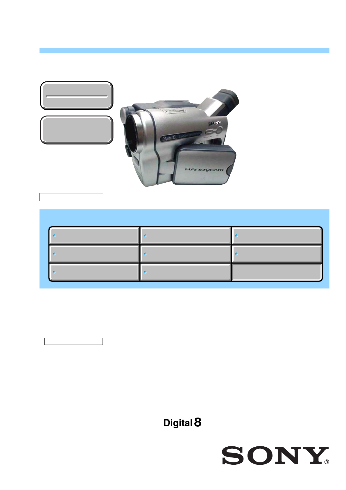
DCR-TRV255E/TRV260/TRV265/TRV265E
SERVICE MANUAL
Ver 1.3 2005.07
Revision History
Revision History
How to use
How to use
Acrobat Reader
Acrobat Reader
RMT-830
US Model
Canadian Model
DCR-TRV260
AEP Model
UK Model
East European Model
North European Model
DCR-TRV255E/TRV265E
E Model
DCR-TRV260/TRV265/TRV265E
Australian Model
DCR-TRV265E
M2200 MECHANISM
Link
Link
SPECIFICATIONS
SPECIFICATIONS
SERVICE NOTE
SERVICE NOTE
DISASSEMBLY
DISASSEMBLY
NTSC MODEL: DCR-TRV260/TRV265
PAL MODEL: DCR-TRV255E/TRV265E
•For ADJUSTMENTS (SECTION 6), refer to SERVICE MANUAL, ADJ (987629251.pdf).
•For INSTRUCTION MANUAL, refer to SERVICE MANUAL, LEVEL 1 (987629241.pdf).
•For MECHANISM ADJUSTMENTS, refer to the “8mm Video MECHANICAL ADJUSTMENT MANUAL IX
M2000 MECHANISM ” (9-929-861-11).
• Reference No. search on printed wiring boards is available.
•Table for differences of function of each model.
•TO TAKE OUT A CASSETTE WHEN NOT EJECT (FORCE EJECT)
•When the machine needs to be repaired, make sure to follow the items of “LCD TYPE CHECK”.
• Changing the data is needs when IC4501 is replaced, make sure to follow the items of “CHANGE OF IC4501”.
• HELP: Sheet attachment positions and procedures of processing the flexible boards/harnesses are shown.
Photo: DCR-TRV265
BLOCK DIAGRAMS
BLOCK DIAGRAMS
FRAME SCHEMATIC DIAGRAMS
FRAME SCHEMATIC DIAGRAMS
SCHEMATIC DIAGRAMS
SCHEMATIC DIAGRAMS
PRINTED WIRING BOARDS
PRINTED WIRING BOARDS
REPAIR PARTS LIST
REPAIR PARTS LIST
DCR-TRV265/TRV265E
Tourist Model
VIDEO CAMERA RECORDER

DCR-TRV255E/TRV260/TRV265/TRV265E
S
SPECIFICATIONS
TM
SERIE
Video camera recorder
System
Video recording system
2 rotary heads, Helical scanning system
Audio recording system
Rotary heads, PCM system
Quantization: 12 bits (Fs 32 kH z, ster eo 1,
stereo 2), 16 bits (Fs 48 kHz, stereo)
Video signal
DCR-TRV260/265:
NTSC color, EIA standards
DCR-TRV255E/265E:
PA L c o lor, CCIR standards
Usable cassette
8 mm video format cassette
Tape speed
DCR-TRV260/265:
SP: Approx. 28.67 mm/s
LP: Approx. 19.11 mm/s
DCR-TRV255E/265E:
SP: Approx. 28.70 mm/s
LP: Approx. 19.13 mm/s
Recording/playback time
DCR-TRV260/265:
(using 120 min. Digital8 video cassette)
DCR-TRV255E/265E:
(using 90 min. Digital8 video cassette)
1 h
SP:
LP: 1 h 30 min
Fast forward/rewind time
DCR-TRV260/265:
(using 120 min. Digital8 video cassette)
DCR-TRV255E/265E:
(using 90 min. Digital8 video cassette)
Approx. 5 min
Viewfinder
Electric vie wfi nder (monochrome )
Image device
3.0 mm (1/6 type) CCD (Charge Coupled
Device)
DCR-TRV260/265:
Gross: Approx. 460 000 pixels
Effective: Approx. 290 000 pixels
DCR-TRV255E/265E:
Gross: Approx. 540 000 pixels
Effective: Approx. 350 000 pixels
Lens
Combined power zoom lens
Filter diameter: 37 mm (1 1/2 in.)
20 × (Optical), 990 × (Digital)
F=1.6 - 2.4
Focal length
2.5 - 50 mm (1/8 - 2 in.)
When converted to a 35 mm still camera
42 - 840 mm (1 11/16 - 33 1/8 in.)
Color temperature
Auto
Minimum illumi n ation
4 lx (lux) (F 1.6)
0 lx (lux) (in the NightShot plus mode)*
*Objects unable to be seen due to the dark can be
shot with infrared lighting.
Input/Output connectors
S video output
4-pin mini DIN
Luminance signal: 1 Vp-p, 75 Ω (ohms),
unbalanced
Chrominance signal:
DCR-TRV260/265: 0.286 Vp-p
DCR-TRV255E/265E: 0.3 Vp-p
75 Ω (ohms), unbalanced
Audio/Video output
AV M I NIJACK
Video signal: 1 Vp-p, 75 Ω: (ohms),
unbalanced, sync negative
Audio signal: 327 mV (at output impedance
more than 47 kΩ: (kilohms)), Output
impedance with less than 2.2 kΩ: (kilohms)
Stereo minijack (ø 3.5 mm)
DV input/output
DCR-TRV260/265/265E:
4-pin connector
DV ou tput
DCR-TRV255E:
4-pin connector
USB jack
mini-B
LCD screen
Picture
6.2 cm (2.5 type)
Total dot number
123 200 (560 × 220)
General
Power requirements
DC 7.2 V (battery pack)
DC 8.4 V (AC Adaptor)
Average power consumption (when using the
battery pack)
During camera recording using viewfin der
2.5 W
During camera recording using L CD
3.4 W
Operating temperature
0°C to 40°C (32°F to 104°F)
Storage temperature
-20°C to + 60°C (-4°F to + 140°F)
Dimensions (approx.)
85 × 98 × 151 mm (3 3/8 × 3 7/8 × 6 in.) (w/h/
d)
Mass (Approx.)
780 g (1 lb 11 oz) main unit only
890 g (1 lb 15 oz) including the
NP-FM30 rechargeable battery pack, Digital8
cassette, lens cap, and shoulder strap
Supplied accessories
AC Adaptor (1)
Power cord (1)
Lens cap (1)
Shoulder strap (1)
Wireless Remote Commander (1)
RMT-830: (DCR-TRV265/265E)
A/V connecting cable (1)
USB cable (1)
Rechargeable battery pack NP-FM30 (1)
CD-ROM “SPVD-012 USB Driver” (1)
21-pin adaptor (1)
: (AEP, UK, EE, NE)
Camera Operating Guide (1)
Computer Application Guide (1)
See page 5-22.
AC Adaptor AC-L15A/L15B
Power requirements
AC 100 - 240 V, 50/60 Hz
Current consumption
0.35 - 0.18 A
Power consumption
18 W
Output voltage
DC 8.4 V, 1.5 A
Operating temperature
0°C to 40°C (32°F to 104°F)
Storage temperature
-20°C to + 60°C (-4°F to + 140°F)
Dimensions (approx.)
56 × 31 × 100 mm (2 1/4 × 1 1/4 × 4 in.) (w/h/
d) excluding the projecting parts
Mass (approx.)
190 g (6.7 oz) excluding the ma ins lea d
Rechargeable battery pack (NP-FM30)
Maximum output voltage
DC 8.4 V
Output voltage
DC 7.2 V
Capacity
5.0 Wh (700 mAh)
Dimensions (approx.)
38.2 × 20.5 × 55.6 mm
(1 9/16 × 13/16 × 2 1/4 in.) (w/h/d)
Mass (approx.)
65 g (2.3 oz)
Operating temperature
0°C to 40°C (32°F to 104°F)
Type
Lithium ion
Design and specification s are subj ect to cha nge
without notice
— 2 —

DCR-TRV255E/TRV260/TRV265/TRV265E
Table for differences of function
Model DCR-TRV255E DCR-TRV260 DCR-TRV265 DCR-TRV265E Remark
Destination AEP, UK, EE, NE US, CND, E E, JE
Remote commander ✕✕aa
Color system PAL NTSC NTSC PAL
VTR Rec ✕ aaaa: with REC button
DV interface DV OUT DV IN/OUT DV IN/OUT DV IN/OUT
LCD type Please refer to page 1-3 to discriminate the type of LCD (TYPE C or TYPE S).
•Abbreviation
AUS: Australian model
CND: Canadian model
EE : East European model
JE : Tourist model
NE : North European model
AEP, UK, EE, NE,
E, AUS, JE
SAFETY-RELATED COMPONENT WARNING!!
COMPONENTS IDENTIFIED BY MARK 0 OR DOTTED LINE WITH
MARK 0 ON THE SCHEMATIC DIAGRAMS AND IN THE PARTS
LIST ARE CRITICAL TO SAFE OPERATION. REPLACE THESE
COMPONENTS WITH SONY PARTS WHOSE PART NUMBERS
APPEAR AS SHOWN IN THIS MANUAL OR IN SUPPLEMENTS
PUBLISHED BY SONY .
SAFETY CHECK-OUT
After correcting the original service problem, perform the following
safety checks before releasing the set to the customer.
1. Check the area of your repair for unsoldered or poorly-soldered
connections. Check the entire board surface for solder splashes
and bridges.
2. Check the interboard wiring to ensure that no wires are
"pinched" or contact high-wattage resistors.
3. Look for unauthorized replacement parts, particularly
transistors, that were installed during a previous repair. Point
them out to the customer and recommend their replacement.
4. Look for parts which, through functioning, show obvious signs
of deterioration. Point them out to the customer and
recommend their replacement.
5. Check the B+ voltage to see it is at the values specified.
6. Flexible Circuit Board Repairing
•Keep the temperature of the soldering iron around 270˚C
during repairing.
• Do not touch the soldering iron on the same conductor of the
circuit board (within 3 times).
• Be careful not to apply force on the conductor when soldering
or unsoldering.
ATTENTION AU COMPOSANT AYANT RAPPORT
À LA SÉCURITÉ!
LES COMPOSANTS IDENTIFÉS P AR UNE MARQUE 0 SUR LES
DIAGRAMMES SCHÉMA TIQUES ET LA LISTE DES PIÈCES SONT
CRITIQUES POUR LA SÉCURITÉ DE FONCTIONNEMENT. NE
REMPLACER CES COMPOSANTS QUE PAR DES PIÈSES SONY
DONT LES NUMÉROS SONT DONNÉS DANS CE MANUEL OU
DANS LES SUPPÉMENTS PUBLIÉS PAR SONY.
Unleaded solder
Boards requiring use of unleaded solder are printed with the leadfree mark (LF) indicating the solder contains no lead.
(Caution: Some printed circuit boards may not come printed with
the lead free mark due to their particular size.)
: LEAD FREE MARK
Unleaded solder has the following characteristics.
• Unleaded solder melts at a temperature about 40°C higher than
ordinary solder.
Ordinary soldering irons can be used but the iron tip has to be
applied to the solder joint for a slightly longer time.
Soldering irons using a temperature regulator should be set to
about 350°C.
Caution: The printed pattern (copper foil) may peel away if the
heated tip is applied for too long, so be careful!
• Strong viscosity
Unleaded solder is more viscous (sticky, less prone to flow) than
ordinary solder so use caution not to let solder bridges occur such
as on IC pins, etc.
• Usable with ordinary solder
It is best to use only unleaded solder but unleaded solder may
also be added to ordinary solder.
— 3 —

DCR-TRV255E/TRV260/TRV265/TRV265E
TABLE OF CONTENTS
Section Title Page Section Title Page
1. SERVICE NOTE
1-1. Note for Repair ································································1-1
1-2. Power Supply During Repairs ·········································1-1
1-3. To Take Out a Cassette when not Eject (Force Eject) ·····1-2
1-4. LCD T ype Check·····························································1-3
1-5. Self-diagnosis Function···················································1-4
1-5-1.Self-diagnosis Function ··················································· 1-4
1-5-2.Self-diagnosis Display·····················································1-4
1-5-3.Service Mode Display ·····················································1-4
1-5-4.Self-diagnosis Code Table ··············································· 1-5
1-6. Change of IC4501 ···························································1-6
2. DISASSEMBLY
2-1. Flow Chart·······································································2-1
2-2. Mechanism Deck Service Position··································2-3
2-3. LCD Service Position ······················································2-5
2-4. Circuit Boards Location ·················································· 2-6
2-5. Flexible Boards Location ················································ 2-7
3. BLOCK DIAGRAMS
3-1. Overall Block Diagram (1/5)··········································· 3-1
3-2. Overall Block Diagram (2/5)··········································· 3-3
3-3. Overall Block Diagram (3/5)··········································· 3-5
3-4. Overall Block Diagram (4/5)··········································· 3-7
3-5. Overall Block Diagram (5/5)··········································· 3-9
3-6. Power Block Diagram (1/2)···········································3-11
3-7. Power Block Diagram (2/2)···········································3-13
5. REPAIR PARTS LIST
5-1. Exploded V iews ····························································5-2
5-1-1. Overall Assembly··························································5-2
5-1-2. Front Panel Block ·························································5-3
5-1-3. Lens Block ····································································5-4
5-1-4. LCD Block ····································································5-5
5-1-5. Cabinet R Block ····························································5-6
5-1-6. EVF Block ····································································5-7
5-1-7. Battery Panel Block ······················································ 5-8
5-1-8. MD Frame Block ·························································· 5-9
5-1-9. Cassette Compartment Assembly, Drum Assembly ···5-10
5-1-10. LS Chassis Block Assembly ·······································5-11
5-1-11. Mechanical Chassis Block Assembly-1 ······················5-12
5-1-12. Mechanical Chassis Block Assembly-2 ······················5-13
5-2. Electrical Parts List ·····················································5-14
4. PRINTED WIRING BOARDS AND
SCHEMATIC DIAGRAMS
4-1. Frame Schematic Diagram ··············································4-1
4-2. Schematic Diagrams························································4-5
CD-471 (CCD IMAGER)················································4-7
VC-344 (1/10)
(A/D CONVERTER, TIMING GENERATOR)··············4-9
VC-344 (2/10)
(DV SIGNAL PROCESS, LENS CONTROL,
STEADYSHOT, DV INTERFACE, VIDEO OUT) ······4-11
VC-344 (3/10) (LENS DRIVE) ····································4-13
VC-344 (4/10) (REC/PB AMP) ····································4-15
VC-344 (5/10) (SERVO) ···············································4-17
VC-344 (6/10) (CAMERA/MECHA CONTROL) ·······4-19
VC-344 (7/10) (HI CONTROL)····································4-21
VC-344 (8/10) (AUDIO PROCESS)·····························4-23
VC-344 (9/10) (DC CONTROL) ··································4-25
VC-344 (10/10) (CONNECTOR) ·································4-27
PD-204 (LCD DRIVER, BACKLIGHT DRIVE)········· 4-29
SI-041 (JACK)·······························································4-31
FP-792 FLEXIBLE ·······················································4-31
FP-228, FP-299, FP-300, FP-301, FP-302, FP-802
FLEXIBLE ····································································4-33
SS-5100, PR-5100 (CONTROL KEY BLOCK)··········· 4-34
CF-5100 (CONTROL KEY BLOCK)···························4-35
4-3. Printed Wiring Boards ···················································4-39
CD-471 ··········································································4-41
VC-344 ··········································································4-43
PD-204···········································································4-47
SI-041, FP-792 FLEXIBLE ··········································4-49
FP-228, FP-299, FP-300, FP-301, FP-302, FP-802
FLEXIBLE ····································································4-51
4-4. Mounted Parts Location ················································ 4-53
— 4 —
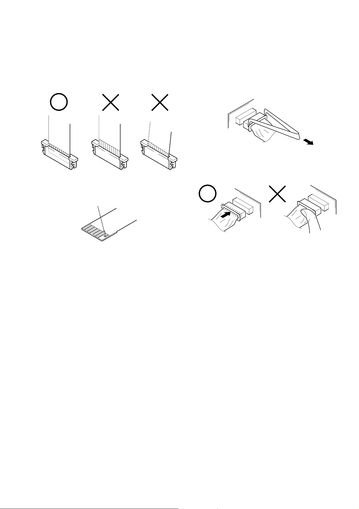
1-1. NOTE FOR REPAIR
When installing a connector, don’t press down at wire of connector.
It is possible that a wire is snapped.
DCR-TRV255E/TRV260/TRV265/TRV265E
SECTION 1
SERVICE NOTE
Make sure that the flat cable and flexible board are not cracked of
bent at the terminal.
Do not insert the cable insufficiently nor crookedly.
Cut and remove the part of gilt
which comes off at the point.
(Be careful or some
pieces of gilt may be left inside)
When remove a connector, don’t pull at wire of connector.
It is possible that a wire is snapped.
1-2. POWER SUPPLY DURING REPAIRS
In this unit, about 10 seconds after power is supplied to the battery terminal using the regulated power supply (8.4V), the po wer is shut of f so
that the unit cannot operate.
The following method is available to prevent this.
Method 1.
Use the AC power adaptor (AC-L10, AC-VQ800 etc.).
1-1
DCR-TRV255E/TRV260/TRV265/TRV265E
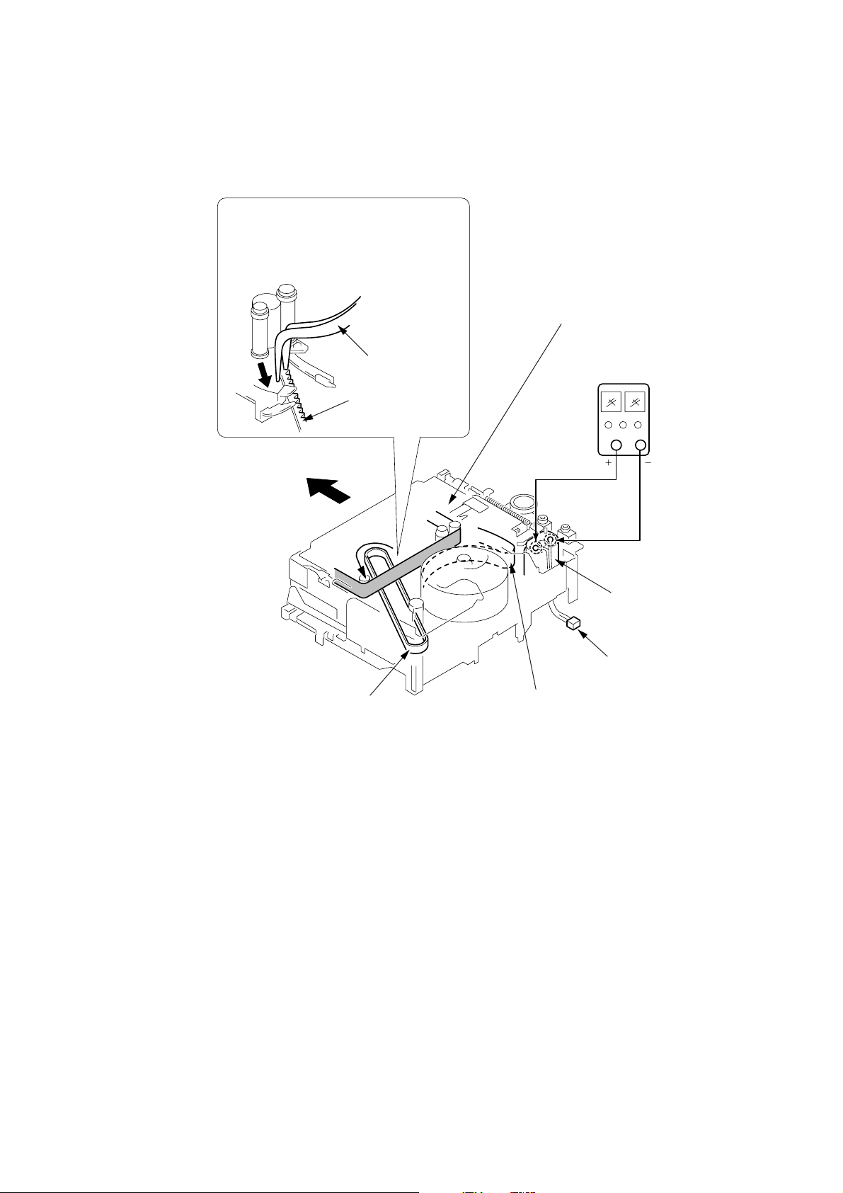
1-3. TO TAKE OUT A CASSETTE WHEN NOT EJECT (FORCE EJECT)
1 Refer to “SECTION 2. DISASSEMBLY” to remove the mechanism deck block.
2 Disconnect CN2401 (2P) of VC-344 board.
3 Add +5V from the DC POWER SUPPLY and unload with a pressing the cassette compartment.
4 Pull the timing belt in the direction of
arrow A with a pincette while pressing
the cassette compartment (take care
not to damage) to adjust the bending
of a tape.
Press the cassette compartment not to
rise the cassette compartment
5 Let go your hold the cassette
compartment and rise the cassette
compartment to take out a cassette.
A
Timing belt
A
Timing belt
Pincette
[DC power supply]
(+5V)
Loading motor
Disconnect CN2401
of VC-344 board.
Adjust the bending of a tape
1-2
DCR-TRV255E/TRV260/TRV265/TRV265E
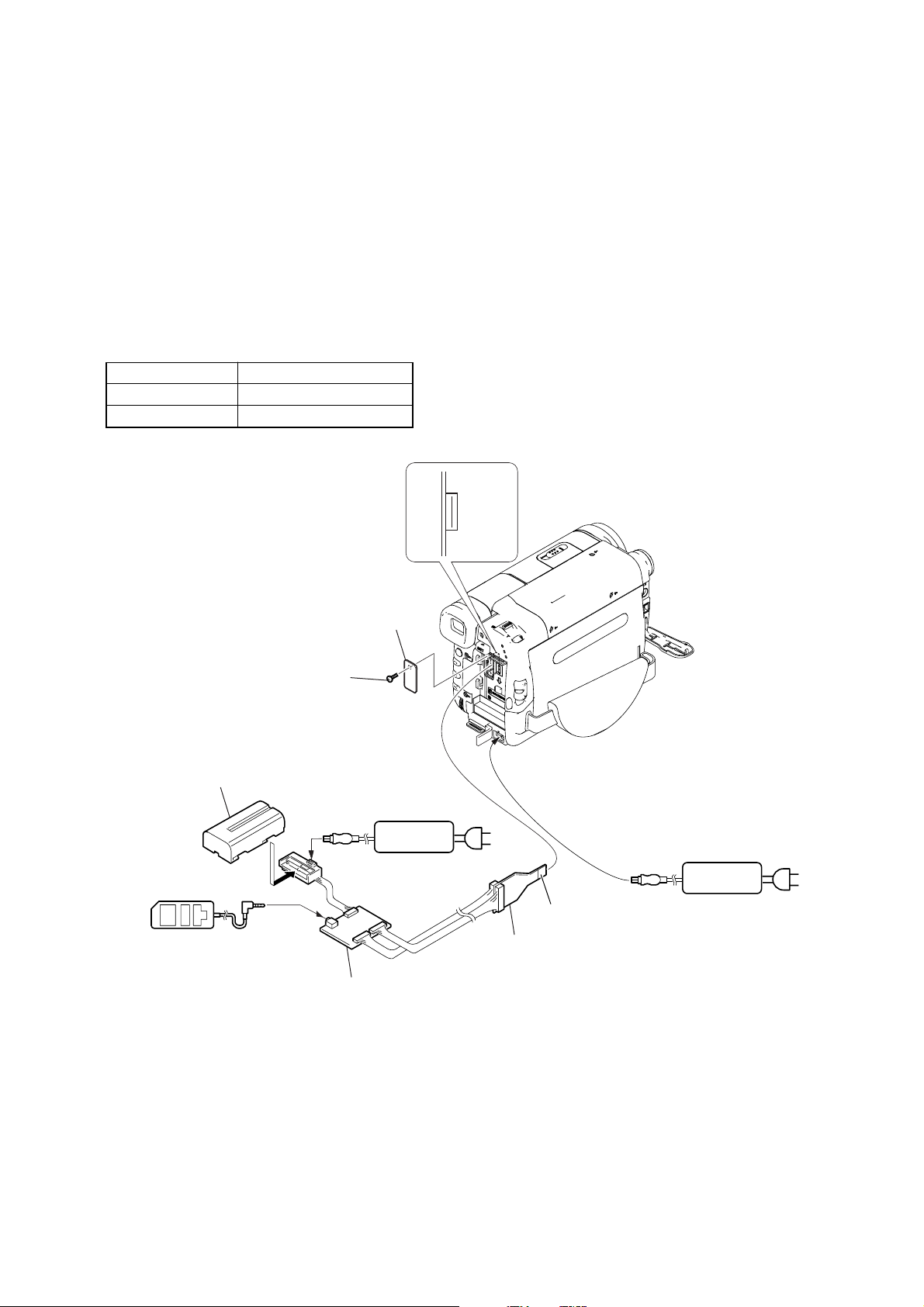
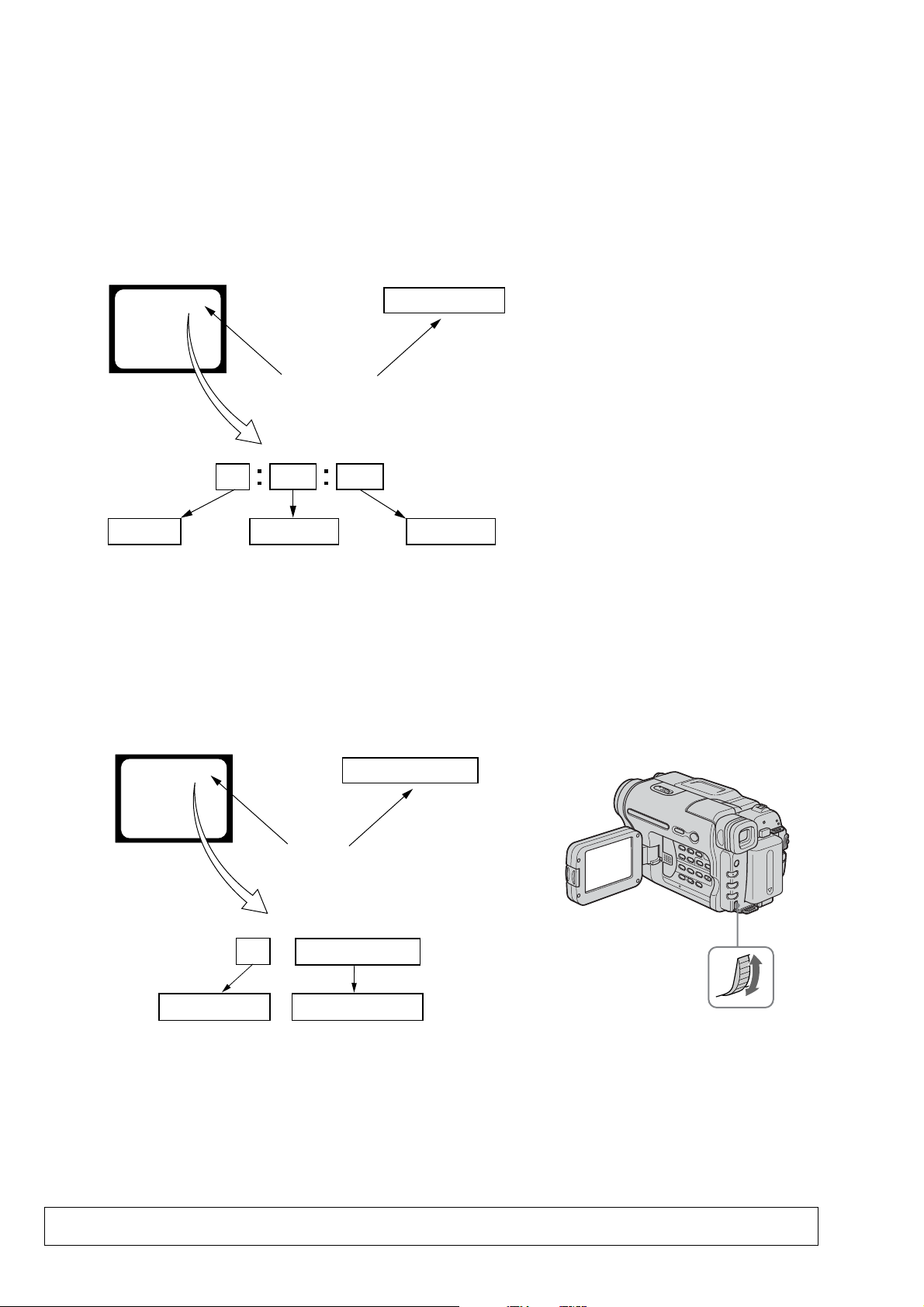
1-4. LCD TYPE CHECK
The LCD type can be checked with data value by connecting the adjustment remote commander.
Note: About PD-204 board and LCD module, discriminate LCD type on the machine, and replace the same type.
Preparations:
1) Connect the equipment for adjustments according to Fig. 1.
2) Connect the adjustment remote commander to VC-344 board CN1011 via I/F unit for LANC control (J-6082-521-A) and CPC jig
connector (J-6082-539-A).
To operate the adjustment remote commander, connect the A C po wer adaptor to the DC IN jack of I/F unit for LANC control, or connect
the L series Info-LITHIUM battery to the battery terminal of I/F unit for LANC control.
Checking method:
1) Select page: 3, address: CC.
2) By checking the data value of display data, the type of LCD can be discriminated.
Data LCD type
64 to 67 TYPE C
40 to 43 TYPE S
CN1011
1
Screw (M2)
L serices Info
LITHIUM battery (7.2Vdc)
LANC jack
Adjustment
remote commander (RM-95)
CPC lid
AC adaptor
16
AC IN
Conductor side
CPC jig connector
(J-6082-539-A)
AC adaptor
AC IN
I/F unit for LANC control
(J-6082-521-A)
1-3
DCR-TRV255E/TRV260/TRV265/TRV265E
1-5. SELF-DIAGNOSIS FUNCTION
1-5-1. Self-diagnosis Function
When problems occur while the unit is operating, the self-diagnosis
function starts working, and displays on the viewfinder or Display
window what to do. This function consists of two display; selfdiagnosis display and service mode display.
Details of the self-diagnosis functions are provided in the Instruction
manual.
Viewfinder Display window
C : 3 1 : 1 1
Repaired by:
C : Corrected by customer
H : Corrected by dealer
E : Corrected by service
engineer
Blinks at 3.2Hz
C
Indicates the appropriate
step to be taken.
E.g.
31 ....Reload the tape.
32 ....Tur n o n power again.
3 1
Block
1 1
C : 3 1 : 11
Refer to “1-5-4. Self-diagnosis Code Table”.
1-5-2. Self-diagnosis Display
When problems occur while the unit is operating, the counter of the
viewfinder or Display window shows a 4-digit display consisting
of an alphabet and numbers, which blinks at 3.2 Hz. This 5-character
display indicates the “repaired by:”, “block” in which the problem
occurred, and “detailed code” of the problem.
Detailed Code
1-5-3. Service Mode Display
The service mode display shows up to six self-diagnosis codes shown in the past.
1. Display Method
While pressing the “STOP” key, set the switch from OFF to “ON”, and continue pressing the “STOP” key for 5 seconds continuously. The
service mode will be displayed, and the counter will show the backup No. and the 5-character self-diagnosis codes.
Viewfinder
[3] C : 3 1 : 1 1
[3]
Backup No.
Order of previous errors
Lights up
C : 3 1 : 1 1
Self-diagnosis Codes
Display window
3 C : 3 1 : 11
Control Dial
2. Switching of Backup No.
By rotating the control dial, past self-diagnosis codes will be shown in order. The backup No. in the [] indicates the order in which the
problem occurred. (If the number of problems which occurred is less than 6, only the number of problems which occurred will be shown.)
[1] : Occurred first time [3] : Occurred third time [5] : Occurred fifth time
[2] : Occurred second time [4] : Occurred fourth time [6] : Occurred the last time
3. End of Display
Turning OFF the power supply will end the service mode display.
Note: The “self-diagnosis display” data will not be erased (reset), when the lithium battery (CONTROL KEY BLOCK (CF-
5100): BT001) is removed.
1-4

1-5-4. Self-diagnosis Code Table
Self-diagnosis Code
DCR-TRV255E/TRV260/TRV265/TRV265E
Repaired by:
C
C
C
C
C
C
C
C
C
C
C
C
C
C
C
C
C
C
C
C
C
C
C
C
C
C
C
C
C
Block
Function
04
21
22
31
31
31
31
31
31
31
31
31
31
31
31
31
32
32
32
32
32
32
32
32
32
32
32
32
32
Detailed
Code
00
00
00
10
11
20
21
22
23
30
31
40
41
42
43
44
10
11
20
21
22
23
30
31
40
41
42
43
44
Symptom/State
Non-standard battery is used.
Condensation.
Video head is dirty.
LOAD direction. Loading does not
complete within specified time
UNLOAD direction. Loading does not
complete within specified time
T reel side tape slacking when unloading
S reel
side tape slacking when unloading
T reel fault.
S reel fault.
FG fault when starting capstan.
FG fault during normal capstan operations.
FG fault when starting drum.
PG fault when starting drum.
FG fault during normal drum operations.
PG fault during normal drum operations.
Phase fault during normal drum operations.
LOAD direction loading motor time-
out.
UNLOAD direction loading motor
time-out.
T reel side tape slacking when
unloading.
S reel side tape slacking when
unloading.
T reel fault.
S reel fault.
FG fault when starting capstan.
FG fault during normal capstan
operations.
FG fault when starting drum.
PG fault when starting drum.
FG fault during normal drum
operations.
PG fault during normal drum
operations.
Phase fault during normal drum
operations.
Correction
Use the InfoLITHIUM battery.
Remove the cassette, and insert it again after one hour.
Clean with the optional cleaning cassette.
Load the tape again, and perform operations from the beginning.
Load the tape again, and perform operations from the beginning.
.
Load the tape again, and perform operations from the beginning.
.
Load the tape again, and perform operations from the beginning.
Load the tape again, and perform operations from the beginning.
Load the tape again, and perform operations from the beginning.
Load the tape again, and perform operations from the beginning.
Load the tape again, and perform operations from the beginning.
Load the tape again, and perform operations from the beginning.
Load the tape again, and perform operations from the beginning.
Load the tape again, and perform operations from the beginning.
Load the tape again, and perform operations from the beginning.
Load the tape again, and perform operations from the beginning.
Remove the battery or power cable, connect, and perform
operations from the beginning.
Remove the battery or power cable, connect, and perform
operations from the beginning.
Remove the battery or power cable, connect, and perform
operations from the beginning.
Remove the battery or power cable, connect, and perform
operations from the beginning.
Remove the battery or power cable, connect, and perform
operations from the beginning.
Remove the battery or power cable, connect, and perform
operations from the beginning.
Remove the battery or power cable, connect, and perform
operations from the beginning.
Remove the battery or power cable, connect, and perform
operations from the beginning.
Remove the battery or power cable, connect, and perform
operations from the beginning.
Remove the battery or power cable, connect, and perform
operations from the beginning.
Remove the battery or power cable, connect, and perform
operations from the beginning.
Remove the battery or power cable, connect, and perform
operations from the beginning.
Remove the battery or power cable, connect, and perform
operations from the beginning.
1-5
DCR-TRV255E/TRV260/TRV265/TRV265E
Self-diagnosis Code
Repaired by:
E
E
Block
Function
61
61
Detailed
Code
00
10
Symptom/State
Difficult to adjust focus
(Cannot initialize focus.)
Zoom operations fault
(Cannot initialize zoom lens.)
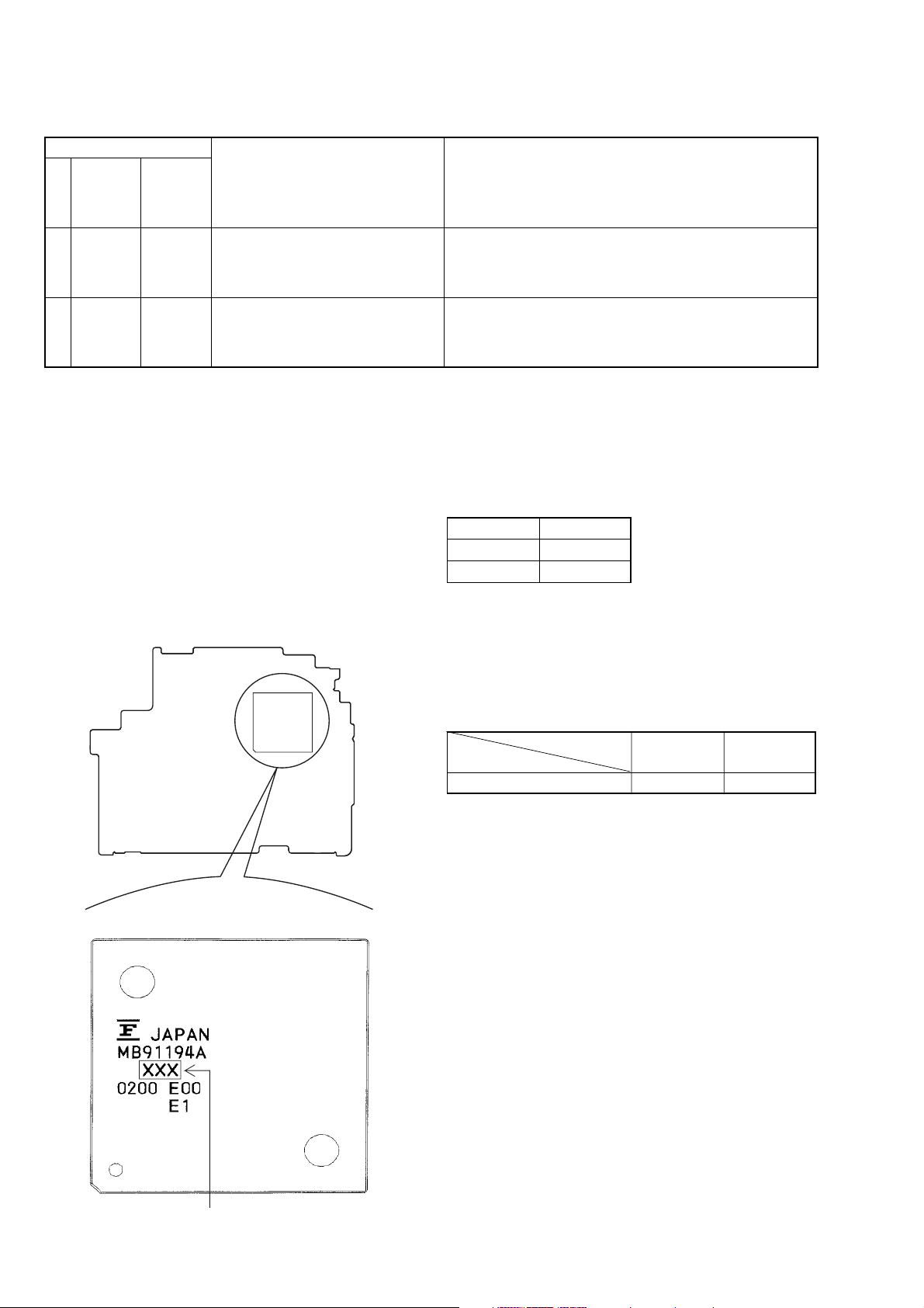
1-6. CHANGE OF IC4501
Due to the change of IC4501 (mechanism control), there are two
types of versions A and B
The EEPROM data are different according to respective versions.
Also, the IC4501 version can be checked by a discrimination method
by the model name or by the adjusting remote commander.
Note 1: Changing the version does not make any changes in
schematic diagrams and the rest.
Note 2: Make it sure to confirm the version after replacing IC4501.
1. Discrimination method by the model name of
IC4501 (mechanism control)
VC-344 BOARD (SIDE A)
IC4501
Correction
Inspect the lens block focus reset sensor (Pin qs of CN1551 of
VC-344 board) when focusing is performed when the control dial
is rotated in the focus manual mode and the focus motor drive circuit
(IC1553 of VC-344 board) when the focusing is not performed.
Inspect the lens block zoom reset sensor (Pin qg of CN1551 of
VC-344 board) when zooming is performed when the zoom switch
is operated and the zoom motor drive circuit (IC1553 of VC-344
board) when zooming is not performed.
2. Discrimination method by adjusting remote
commander
Version check method:
1) Select page: 3, and address: FF.
2) The version of IC4501 can be checked from the displayed data.
Data Version
01 A
02 B
Data change method:
1) Select page: 0, address: 01, and set data: 01.
2) Select page: 1C, and input the data in the following table.
Note: To write in the non-volatile memory (EEPROM), press the
PAUSE button of the adjustment remote commander each
time to set the data.
3) Select page: 0, address: 01, and set data: 00.
Version
Address
D0 40 42
AB
154 : A
155 : B
1-6E
DCR-TRV255E/TRV260/TRV265/TRV265E
SECTION 2
DISASSEMBLY
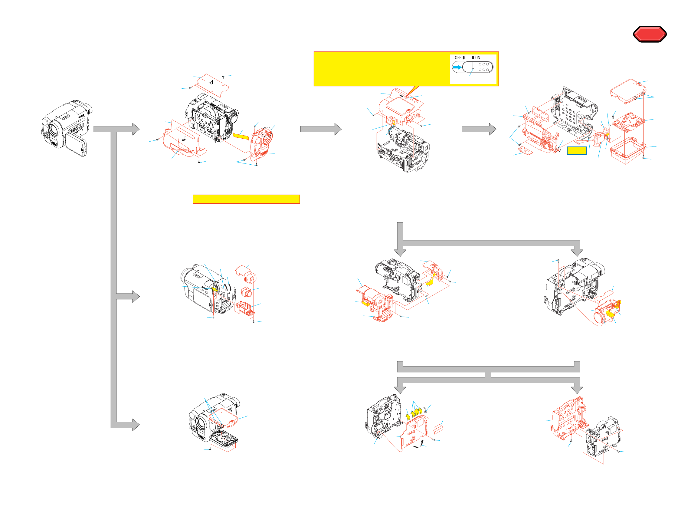
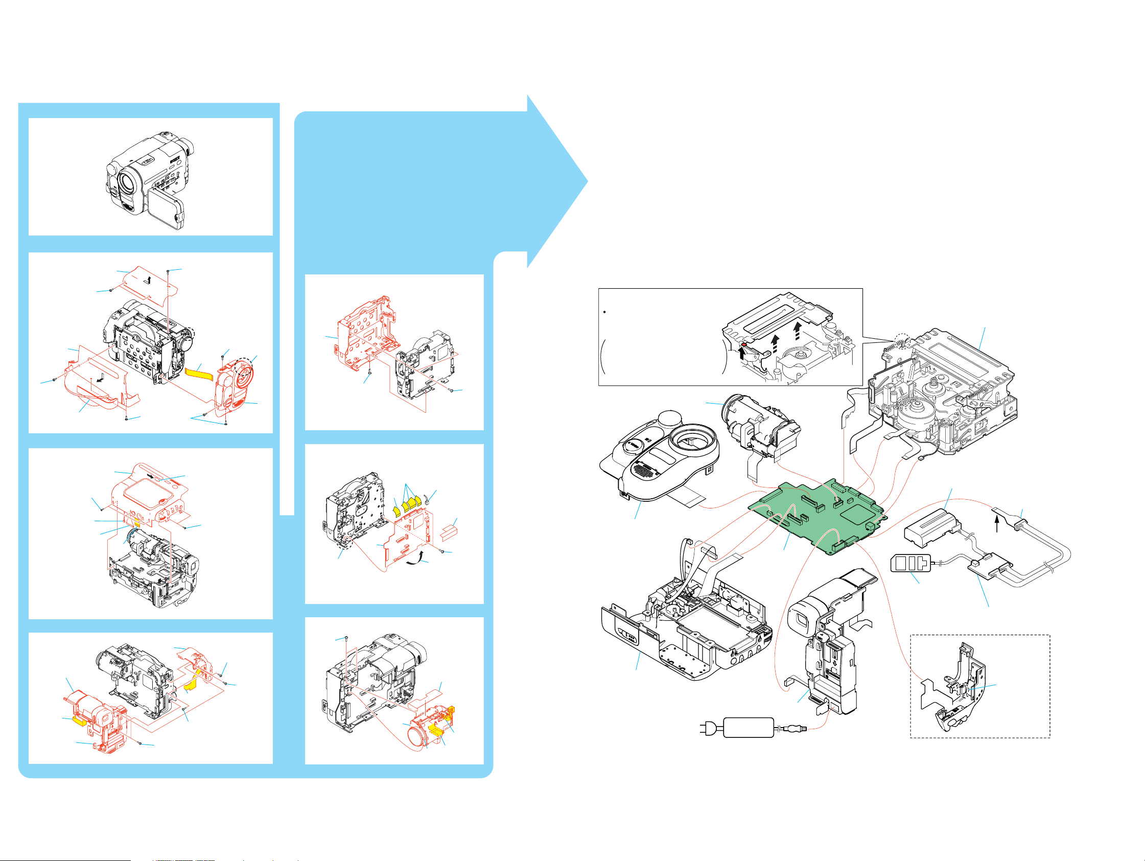
2-1. FLOW CHART
The following flow chart shows the disassembly procedure.
1
5
4
3
1 Lock ace
2 Cabi (upper)
3 Grip belt
4 Lock ace
5 Cabi (L)
x3
x3
2
4
6 Lock ace
1
6
9
6
x3
7 Claw
8 Front panel
Note: Flexible board is connected.
9 FP-796: CN754, CN1001
7
8
Note: When you remove Cabinet (R) Block,
or when you assembly, please slide
NS knob to the position of "ON".
3
1
6
5
4
1 Lock ace
x6
2
1
2 NS knob to the position of "ON".
3 Cabi (R)
4 VC-344: CN1007
5 VC-344: CN1003
6 VC-344: CN1008
NS knob
3
2
5
1
1 Tripod Screw
2 Tapping P2
3 Tapping P2
4 Claw
5 CF-5100
6 Tapping P2
7 Claw
8 P Cabi (C)
x2
4
q;
9
qd
HELP
9 Tapping P2
x2
q; Tapping P2
x6
qa P Cabi (M)
qg
qs
qh
x2
x1
qs PD-204: CN6005
qd PD-204: CN6001
qf PD-204, LCD901, ND901
x4
qg Tapping P2
x4
qh Hinge assy
HELP
HELP
8
7
qf
qa
6
4
7
2
1 Lift up the EVF.
2 Tapping P2
x4
3 Down the EVF.
4 EVF block
2
1
3
5
8
6
2
5 EVF Cabi (upper)
6 EVF Cabi (lower)
7 FP-797: LCD902
8 EVF lens
3
4
1
2
1 VC-344: CN1013
2 VC-344: CN4001
3 Lock ace
x3
4 EVF/Battely panel block
7
8
5
6
3
7
3
5 VC-344: CN1009
6 Tapping P2
7 Lock ace
x1
8 SS-5100
2
3
1
x1
4
6
1 VC-344: CN1501
2 VC-344: CN1551
3 Lens sheet
2
3
1
2
5
4 Lock ace
x2
5 Boss
6 Lens LSV-820A
1
1 Tapping P2
2 Claw
x2
3 P Cabi (C)
2-1 2-2
x4
8
5
1 VF blind sheet
2 VC-344: CN2403, CN2404, CN3201
3 VC-344: CN2401
4 Screw (M1.7)
x2
4
6
5 Claw
6 Open the VC-344.
7 VC-344: CN2402
8 VC-344
1
1 Screw (M1.7)
2 CS frame
1
x3
DCR-TRV255E/TRV260/TRV265/TRV265E
2-2. MECHANISM DECK SERVICE POSITION
Connection to Check the Mechanism deck
To check the mechanism deck, set the Camera or VTR to the "Forced power ON" mode. (Or, connect the control key
block (SS-5100) to the CN1009 of VC-344 board and set the power switch to the "CAMERA" or "PLAY/edit" position.)
Operate the Camera functions of the zoom and focus, the VTR function using the adjustment remote commander
(with the HOLD switch set in the OFF position).
4
5
3
1
2
4
6
1
9
6
7
8
2
1
1
Setting the "Forced Camera Power ON" mode
1) Select page: 0, address: 01, and set data: 01.
2) Select page: D, address: 10, set data: 02 and
press the PAUSE button of the adjustment remote
commander.
Setting the "Forced VTR Power ON" mode
1) Select page: 0, address: 01, and set data: 01.
2) Select page: D, address: 10, set data: 02 and
press the PAUSE button of the adjustment remote
commander.
How to move up the cassette
compartment manually
Press the cassette compartment
in the direction of the arrow A
to move it up in the direction of
the arrow B.
Lens block
A
B
Exiting the "Forced Power ON" mode
1) Select page: 0, address: 01, and set data: 01.
2) Select page: D, address: 10, data: 00, and press the PAUSE
button of the adjustment remote commander.
3) Select page: 0, address: 01, and set data: 00.
Mechanism deck
1
4
2
1
6
5
3
4
3
8
2
5
6
1
7
3
4
5
8
7
6
2
5
6
3
3
2
1
4
1
Front panel block
Cabinet R block
EVF block/
Battery panel block assembly
AC IN
AC adaptor
VC-344 board
Info lithium battery
(L series)
CPC jig connector
(J-6082-539-A)
Contacting
surface
Adjustment remote
commander (RM-95)
I/F unit for LANC control
(J-6082-521-A)
Eject switch
Control key block
(SS-5100)
When exiting the "Forced Power ON" mode, connect the control
key block (SS-5100) to the CN1009 of VC-344 board. Or, when
ejecting the cassette, connect the control key block (SS-5100) to
the CN1009 of VC-344 board. and press the Eject switch.
2-3 2-4
2-3. LCD SERVICE POSITION
AC adaptor
AC IN
AC adaptor
I/F unit for LANC control
(J-6082-521-A)
CPC jig connector
(J-6082-539-A)
CPC jig connector
L serices Info
LITHIUM battery (7.2Vdc)
LCD panel
PD-204 board
Back light unit
Adjustment
remote commander (RM-95)
Conductor side
CN1011
1
16
LANC jack
AC IN
2
1
3
DCR-TRV255E/TRV260/TRV265/TRV265E
2-5
DCR-TRV255E/TRV260/TRV265/TRV265E
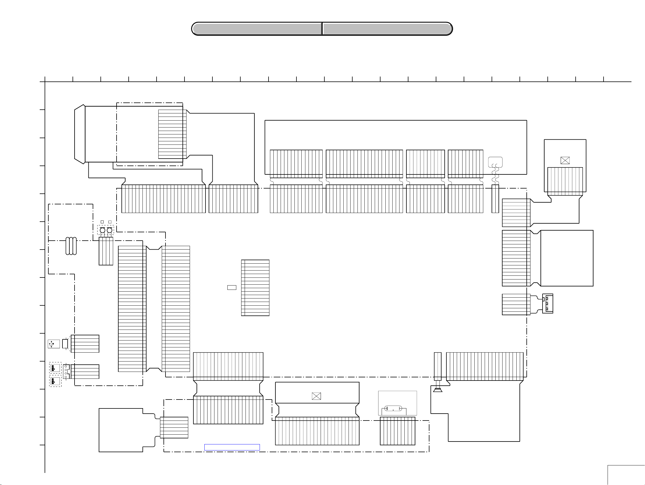
2-4. CIRCUIT BOARDS LOCATION
VC-344
SI-041
CD-471
PD-204
Board Name Function
CD-471 CCD IMAGER
VC-344 A/D CONVERTER, TIMING GENERATOR, DV SIGNAL PROCESS, LENS
CONTROL, STEADYSHOT, DV INTERFACE, VIDEO OUT, LENS DRIVE,
REC/PB AMP, SERVO, CAMERA/MECHA CONTROL, HI CONTROL,
AUDIO PROCESS, DC CONTROL, CONNECTOR
PD-204 LCD DRIVE, BACKLIGHT DRIVE
SI-041 JACK
2-6
2-5. FLEXIBLE BOARDS LOCATION
DCR-TRV255E/TRV260/TRV265/TRV265E
FP-792
FP-796
FFC-005
FP-797
PR-5100
SS-5100
CF-5100
2-7E
DCR-TRV255E/TRV260/TRV265/TRV265E
HELP
Sheet attachment positions and procedures of processing the flexible boards/harnesses are shown.
Harness (PD-124)
Claw
Claw
Note: Close the LCD panel, when you work.
HELP

Link
Link
DCR-TRV255E/TRV260/TRV265/TRV265E
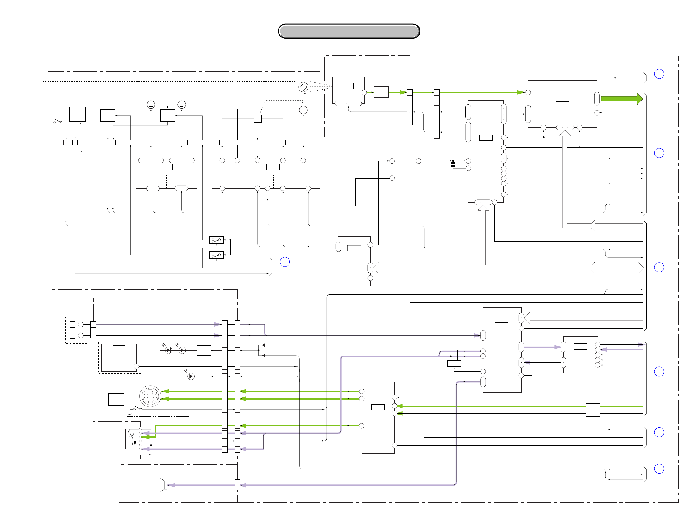
3. BLOCK DIAGRAMS
OVERALL BLOCK DIAGRAM (1/5)
OVERALL BLOCK DIAGRAM (1/5)
OVERALL BLOCK DIAGRAM (2/5)
OVERALL BLOCK DIAGRAM (2/5)
OVERALL BLOCK DIAGRAM (3/5)
OVERALL BLOCK DIAGRAM (3/5)
OVERALL BLOCK DIAGRAM (4/5)
OVERALL BLOCK DIAGRAM (4/5)
OVERALL BLOCK DIAGRAM (5/5)
OVERALL BLOCK DIAGRAM (5/5)
POWER BLOCK DIAGRAM (1/2)
POWER BLOCK DIAGRAM (1/2)
POWER BLOCK DIAGRAM (2/2)
POWER BLOCK DIAGRAM (2/2)
DCR-TRV255E/TRV260/TRV265/TRV265E
SECTION 3
BLOCK DIAGRAMS
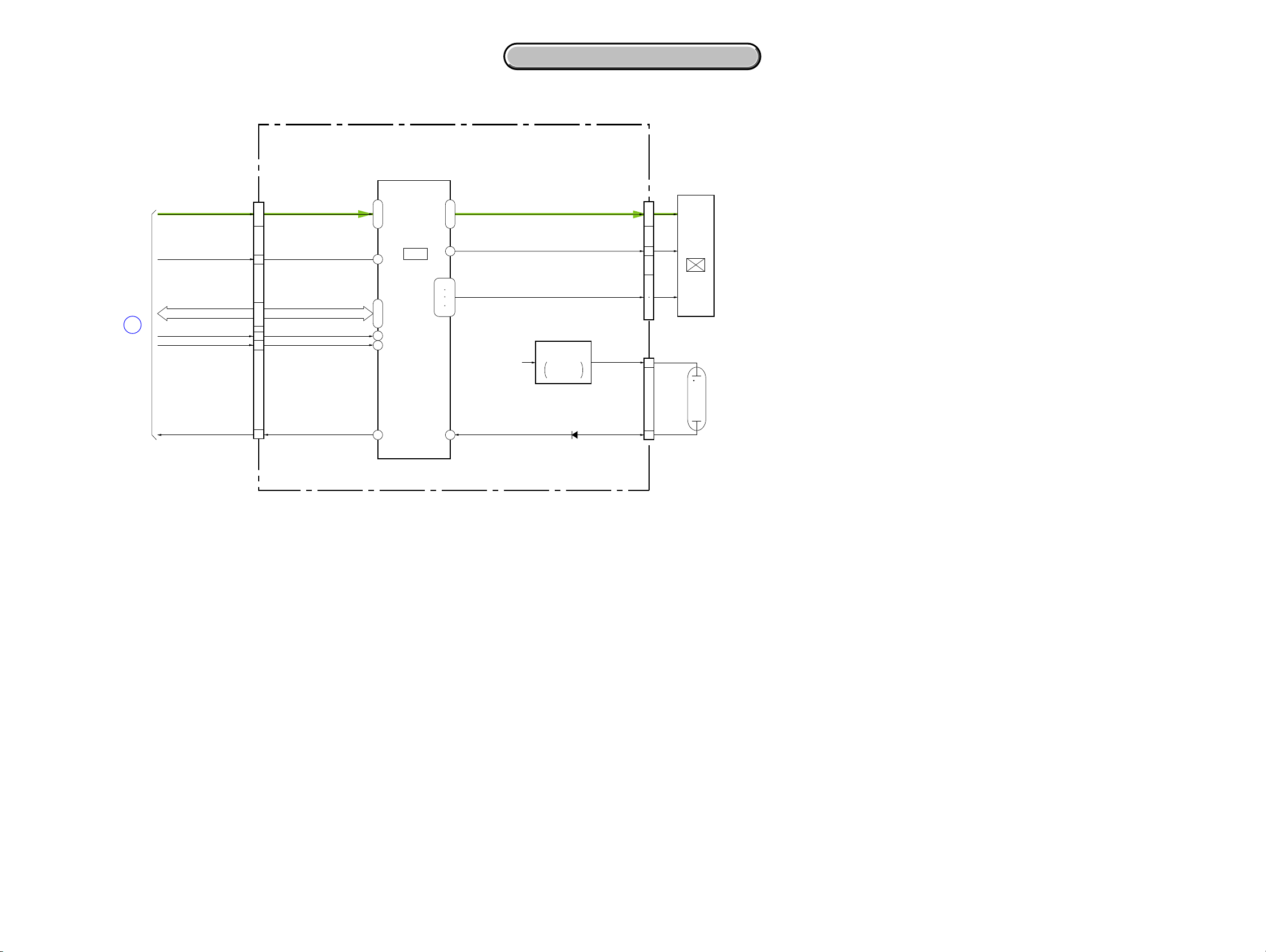
3-1. O VERALL BLOCK DIAGRAM (1/5)
LENS ASSY
ZOOM MOTOR
NIGHT
SHOT
CN1551
LENS
TEMP
SENSOR
5 15 12 21 19
17 18
TEMP
IR SWITCH
XNS SW
D 2.8V
ZOOM
SENSOR
FC SENS OUT
ZM SENS OUT
ZM RST
FC RST
MM MM
10 – 7
ZM SENSE
VCC
5717 19 24
ZOOM
MOTOR
DRIVE
13 – 16
SI-041 BOARD (1/3)
FOCUS
SENSOR
ZOOM
A,B,XA,XB
IC1553
(3/10)
LD EN1
LD DIR1A
LD DIR1B
FOCUS MOTOR
1 – 4
FOCUS
MOTOR
DRIVE
9 – 12
3. BLOCK DIAGRAMS
3. BLOCK DIAGRAMS
( ) : Number in parenthesis ( ) indicates the division number of schematic diagram where the component is located.
CD-471 BOARD VC-344 BOARD (1/4)
FOCUS
A,B,XA,XB
21 23
LD EN0
LD DIR0A
LD DIR0B
1316
FC SENSE
VCC
Q1555 (1/2)
IRIS
BIAS(+)
1
HALL
BIAS
HALL
REF
Q1555 (2/2)
2322
IRIS
HALL(+)
2
HALL
OFFSET
D 2.8V
ZM RST LED
LENS TEMP AD
H
IRIS
HALL(-)
5
HALL
AMP
6
FC RST LED
IC1552
(3/10)
73
HALL
AD
OVERALL (3/5)
(PAGE 3-5)
20
14
HALL
GAIN
12
IRIS
BIAS(-)
HALL
GAIN
7
IRIS
IRIS
METER
MM
IRIS DRIVE(-)
8
IRIS
DRIVE
10
IRIS PWM,
IRIS COM
HALL OFFSET,
HALL GAIN
IC951
CCD
IMAGER
1 – 4 12 – 14
3
IC1601
2
EVR
(D/A CONVERTER)
(3/10)
7
HALL REF
1
6
7
8
Q951
BUFFER
DA STRB
CN951 CN1501
1
7
5
1
11
14
IC1554
(3/10)
XTAL AMP
HALL REG
ı
9
ı
V1-V4,RG,H1,H2
CAM SO, CAM SCK
FREQ TUNE
7
14
6
ı
8
1
ı
4
CCD OUT
RG, H1, H2
V1 – V4
X1501
27MHz
18
21
22
25
26
28
31
4
5
IC1501
TIMING
GENERATOR
(1/10)
35 3738
CLPDM,
PBLK,
1
XSHP,
2
XSHD
15
16
XRST VTR
40
VCK VCK
12
44
45
34
41
48
36
CAM DD ON
42
39
XCS TG
CAM SI, CAM SO, CAM SCK
30
S/H, AGC, A/D CONVERTER
19
21
ı
23
43
IC1502
(1/10)
46 4847
2
ı
11
20
16
CAM SI, CAM SO, CAM SCK
XRST VTR
AD0-AD9
FE CLPOB
TG AHD, TG AVD
TG ZSG1
TG ZV1
TG ID
TG VGAT
LD EN0,EN1,
LD DIR0A,B,
LD DIR1A,B,
FC RST, ZM RST
CS CH, CH SO, CH SCK
CAM DD ON
XCS TG
IRIS PWM, IRIS COM
HALL AD, XNS SW
DA STRB
AV JACK IN
XS JACK IN
VOUT ON
1
OVERALL (3/5)
(PAGE 3-5)
2
OVERALL (2/5)
(PAGE 3-3)
3
OVERALL (3/5)
(PAGE 3-5)
MIC901
L
R
CN753
INT MIC L
1
INT MIC R
3
TRV265/TRV265E
A/V OUT
IC751
REMOTE
COMMANDER
RECEIVER
J751
S VIDEO
OUT
J752
1
(IR EMITTER)
CONTROL KEY BLOCK (CF-5100) (1/2)
SP901
SPEAKER
05
D753, 754
D759
(TALLY)
Y
C
XS JACK IN
V
L
AV JACK IN
R
CN754 (1/3)
Q751
LED
DRIVE
XSIRCS SIG
33
32 5
20
23
25 10
13
11
12
15
18
19
17
CN1001 (1/3)
4
17
14
24
26
25
22
19
18
20
CN1008
1
2
SP+, –
D1009
L
R
IR_ON
SIRCS PWM
SIRCS SIG
XF TALLY LED
XS JACK IN
AV JACK IN
2
VSP SO, XVSP SCK
IC5401
L, R
L
R
Q5401, 5403
Y
11
C
5
IC6501
Y/C MIX
BUFFER
V
(2/10)
6
13
Y Y OUT
14
C C OUT
1
3
MUTE
POWER MUTE
SP+,–
AUDIO
42
PROCESS
46
(8/10)
27
26
25
7
9
3
4
56
58
62
64
13
REC OUT L, R
PB IN L, R
3
2
15
16
IC5402
A/D, D/A
CONVERTER
(8/10)
Q3308
BUFFER
8
9
12
10
11
VSP SO, XVSP SCK
XCS IC 5401
DATA TO SFD
DATA FROM SFD
SFD BCK
SFD LRCK
SFD FCK
BEEP
IR ON
SDC ON
SIRCS PWM
SIRCS SIG
XF TALLY LED
4
OVERALL (2/5)
(PAGE 3-3)
5
OVERALL (3/5)
(PAGE 3-5)
6
OVERALL (4/5)
(PAGE 3-8)
A : VIDEO SIGNAL
A : AUDIO SIGNAL
3-1 3-2
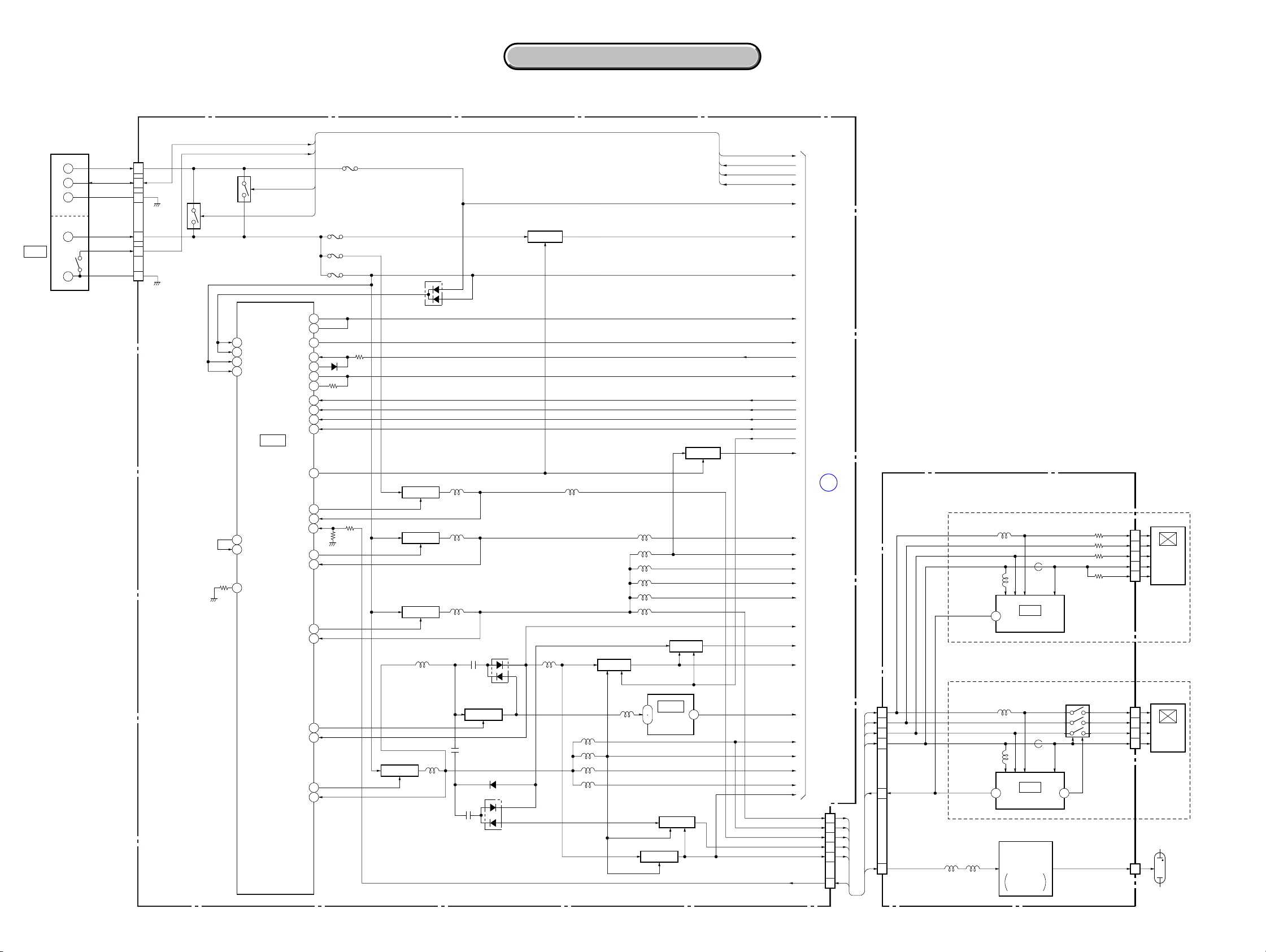
DCR-TRV255E/TRV260/TRV265/TRV265E
3. BLOCK DIAGRAMS
3. BLOCK DIAGRAMS
3-2. O VERALL BLOCK DIAGRAM (2/5)
VC-344 BOARD (2/4)
199
AD0-AD9
FE CLPOB
VCK
TG AHD, TG AVD
2
OVERALL (1/5)
(PAGE 3-2)
8
OVERALL (3/5)
(PAGE 3-6)
9
OVERALL (3/5)
(PAGE 3-5)
10
OVERALL (4/5)
(PAGE 3-8)
4
OVERALL (1/5)
(PAGE 3-2)
05
TG ZSG1
TG ZV1
TG ID
TG VGAT
LD EN0, EN1,
LD DIR0A, B,
LD DIR1A, B
FC RST, ZM RST
SPCK
VFO VD
VFO OE
DRP
SWP
XUSB EN
VREF
LINE OUT VD
XCS VFD
XCS SFD
XCS IC3301
CAM SI, CAM SO, CAM SCK
CAM XCE
XIRQ GEMINI
OSD V
DATA TO SFD
DATA FROM SFD
SFD BCK
SFD LRCK
SFD FCK
Y OUT
C OUT
ı
208
209
216
4
3
214
215
212
213
5
6
8
9
11
12
14
15
141
42
43
161
162
129
181
182
187
188
189
196
195
194
193
197
192
63
64
68
67
69
110
113
IC3301
DV SIGNAL
PROCESS,
D/A CONVERTER,
LENS CONTROL,
STEADYSHOT
(2/10)
( ) : Number in parenthesis ( ) indicates the division number of schematic diagram where the component is located.
TPA+, –,
Q3303
BUFFER
6
ı
9
TPB+, –
RF MON
30
35 28
46
40
42
44
OVERALL (4/5)
(PAGE 3-8)
13
PB Y OUT
2796
BL CONT
IC3201
REC/PB
AMP
(4/10)
USB 3.3V
3
4
10
9
38
37
43
PANEL HD
PANEL VD
PANEL HD
PANEL VD
RF SWP
SW PS
ALL PS
CN1003
(1/2)
CN1013
Q3307
5
ı
7
10
11
ı
VD SO, VD SI, VD SCK
13
9
8
4
6
5
4
2
VIDEO IN
H SYNC
V SYNC
NSLEEP
154
ı
L BUS0-3
157
TRCKO
143
24M
159
USB D+
126
USB D–
127
RF IN
REC DT
77
REC A1, A2
75
76
REC CK
78
ATF LATCH
163
180
FRRV,TRRV,TRRT
179
178
167
MC BUS
ı
176
185
184
VSP SO, VSP SI, XVSP SCK
178
XRST VTR
190
18
VD SO, VD SCK
20
XCS VD
19
119
PANEL R, G, B PANEL R, G, B
121
123
131
PANEL HD, VD
130
BW Y
116
EVF DD ON
117
45
ı
42
47
79
IC3302
DV INTERFACE
(2/10)
29-32 34-37
MC BUS
XCS LCD DA
C-SYNC/XHD
PANEL XVD
BL CONT
Q3202, 3204, 3205
VSP SO, VSP SI, XVSP SCK
EVF BLOCK
LCD902
B/W
LCD UNIT
CN1001
(2/3)
USB D+
USB D–
USB DET
CN1011
(1/3)
RF MON
RF SWP
FRRV
CN3201
ODD (SP1)
EVEN (SP2)
FLYING
ERAE
OSC
USB DET
XUSB ON
ATF LATCH
FRRV, TRRV, TRRT
MC BUS
XRST VTR
VD SO, VD SI, VD SCK
XCS LCD
12
OVERALL (5/5)
(PAGE 3-9)
28
29
31
32
35
34
36
9
5
2
5
4
7
8
11
XFE ON
RF SWP
SW PS
ALL PS
XCS VD
SI-041 BOARD (2/3)
CN754
(2/3)
5
6
8
9
CN752
2
3
D755
1
D+
D–
VCC
M2200 MECHA DECK (1/2)
CPC
(FOR CHECK)
VIDEO HEAD
11
OVERALL (3/5)
(PAGE 3-5)
A : VIDEO SIGNAL
A : AUDIO SIGNAL
A : VIDEO/AUDIO SIGNAL
A : VIDEO/AUDIO/SERVO SIGNAL
SP1
SP2
CN751
TRV260/
TRV265/
DV
(OUT)
TRV265E
TRV255E
DV
(USB)
(IN/OUT)
3
2
1
CH
FLYING
ERASE
CH
3-3 3-4
3. BLOCK DIAGRAMS
3. BLOCK DIAGRAMS
DCR-TRV255E/TRV260/TRV265/TRV265E
3-3. O VERALL BLOCK DIAGRAM (3/5)
VC-344 BOARD (3/4)
OVERALL (1/5)
(PAGE 3-2)
OVERALL (1/5)
(PAGE 3-1)
OVERALL (2/5)
(PAGE 3-4)
OVERALL (2/5)
(PAGE 3-3)
OVERALL (1/5)
(PAGE 3-2)
OVERALL (1/5)
(PAGE 3-2)
11
1
7
9
3
5
XRST VTR
ZM RST LED
FC RST LED
LENS TEMP AD
XFE ON
RF SWP
USB DET
XUSB ON
SW PS
ALL PS
ATF LATCH
FRRV, TRRV, TRRT
MC BUS
VSP SO, VSP SI, XVSP SCK
XRST VTR
VD SO, VD SI, VD SCK
XCS VD
XCS LCD
VFO VD
VFO OE
DRP
SWP
XUSB EN
VREF
LINE OUT VD
XCS VFD
XCS SFD
XCS IC 3301
CAM SI, CAM SO, CAM SCK
CAM XCE
XIRQ GEMINI
CS CH, CH SO, CH SCK
CAM DD ON
XCS TG
IRIS PWM, IRIS COM
HALL AD, XNS SW
CAM SI, CAM SO, CAM SCK
DA STRB
AV JACK IN
XS JACK IN
VOUT ON
VSP SO, XVSP SCK
XCS IC 5401
BEEP
IR ON
SDC ON
Q4502
MODULATOR
Q4501
MODULATOR
MELODY ENV
MELODY CARR
( ) : Number in parenthesis ( ) indicates the division number of schematic diagram where the component is located.
(5/10)
IC2401 (3/3)
XNS SW
HALL AD
34
100
55
57
127
170
172
113
131
29
28
162
23
179
IC4501
178
CAMERA/
45
MECHA
ı
CONTROL
52
(6/10)
32
33
69
70
67
82
83
80
61
38
203
68
163
164
132
204
201
155
215
97
161
208
62
73
71
173
20
94
95
187
128
78
77
75
59
185
186
26
43
98
202
194
209
88
89
197
198
190
119
106
ı
108
15
13
138
31
30
192
193
180
110
109
120
214
181
8
9
63
ı
66
135
169
91
10
87
86
84
3
1
DRUM PWM
CAP PWM
VSP SO, XVSP SCK
XCS IC 2401
DRUM FG
DRUM PG
CAP FG
DEW AD
MODE SW A-C
LOAD
UNLOAD
LM LIM DET
TAPE END
TAPE TOP
T REEL FG
S REEL FG
TAPE LED ON
REC PROOF
ME SW
HI8 MP SW
IC 5001 SO, IC 5001 SI, IC 5001 SCK, XCS IC 5001
V LIGHT PWM
XCS EEP
EEP SI, EEP SO, EEP SCK
X4501
20MHz
44
41
38
36
3716
1
2
5
6
XCS EEP
EEP SI, EEP SO, EEP SCK
LPF
SERIAL
INTERFACE
XCC DOWN
XSYS RST
ZOOM VR AD
CUSTOM LED ON
IC4502
EEPROM
(6/10)
OSD V
SYS V
45
43
35
DRUM ERROR
CAP ERROR
SPCK
14
IN7 (VL 16V)
OVERALL (4/5)
(PAGE 3-8)
(9/10)
25
IC1301 (1/2)
6
DRUM/CAPSTAN
PWM
9
DRIVE
24
OVERALL (2/5)
8
(PAGE 3-3)
Q1001
VIDEO LIGHT
DRIVE
EEP SI, EEP SO, EEP SCK
62
61
XCS EEP
SWITCHING
SWITCHING
CN1001
(3/3)
CN1011
(2/3)
Q1310
Q1309
TAPE LED ON
1 36
16
1
(FOR CHECK)
14
15
CN754(3/3)
CPC
DRUM VS
DRUM FG
DRUM PG
CAP VS
CAP FG
UNLOAD
LM LIM DET
TAPE END
TAPE TOP
T REEL FG
S REEL FG
Q2401
LED DRIVE
SI-041 BOARD
(3/3)
LND754
VL+
64
67
53
50
75
77
4
LOAD,
32
33
31
21 20
19
29
25
FP-792 FLEXIBLE
(5/10)
IC2401 (1/3)
DRUM
MOTOR
DRIVE
FG AMP
PG AMP
CAPSTAN
MOTOR
DRIVE
FG AMP
(5/10)
IC2401 (2/3)
LOADING
MOTOR
DRIVE
TAPE END
DETECT
TAPE TOP
DETECT
T REEL
FG AMP
S REEL
FG AMP
D001 – 003
(VIDEO LIGHT)
63
65
68
52
49
74
76
78
10
ı
15
7
8
69
72
18
26
27
22
23
DRUM U, V, W
CAP U, V, W
HU1, 2
HV1, 2
HW1, 2
FG1, 2
DEW AD
MODE SW A-C
LM (+) , LM (–)
TAPE END (C)
TAPE TOP (C)
T REEL (+) , (–)
S REEL (+) , (–)
TAPE LED (K)
REC PROOF
ME SW
HI8 MP SW
XCC DOWN
CN2402
FG
PG
CN2403
CN2401
CN2404
M2200 MECHA DECK (2/2)
M901
10
ı
5
3
1
14
ı
9
7
ı
2
18
16
22
21
ı
19
2
1
2
1
9
10
7
6
3
13
12
14
15
DRUM MOTOR
M
DRUM FG
DRUM PG
M902
CAPSTAN MOTOR
M
HU, HV, HW
CAPSTAN FG
DEW SENSOR
S901
MODE SWITCH
M903
LOADING MOTOR
M
Q002
TAPE END
SENSOR
Q001
TAPE TOP
SENSOR
T REEL
SENSOR
S REEL
SENSOR
S001
S002
A : SERVO SIGNAL
H001
H002
REC PROOF
ME/MP
HI8 MP
C. C. LOCK
D001
TAPE
LED
05
3-5 3-6
DCR-TRV255E/TRV260/TRV265/TRV265E
3. BLOCK DIAGRAMS
3. BLOCK DIAGRAMS
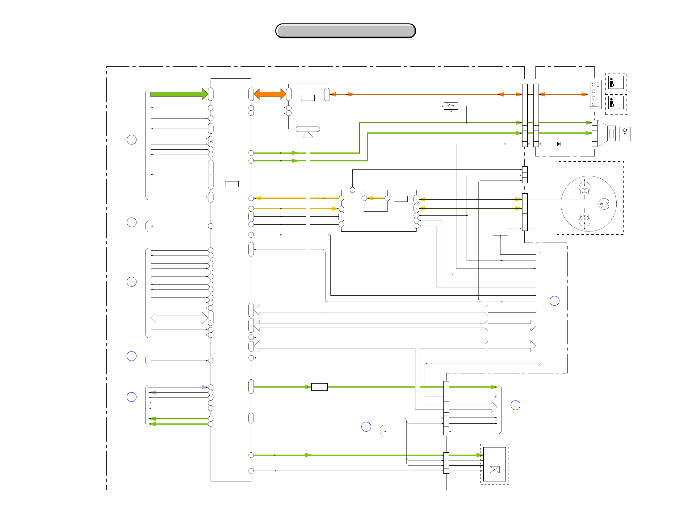
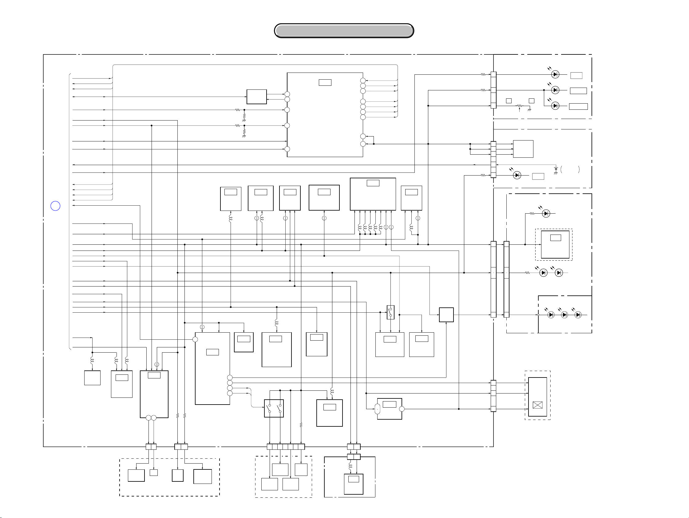
3-4. OVERALL BLOCK DIAGRAM (4/5)
VC-344 BOARD (4/4)
CN1011
(3/3)
12
11
13
CN1003
(2/2)
20
20
CN1009
14
15
1
4
3
16
6
8
9
12
CN1007
19
20
5
14
18
16
6
22
Q1002
LED
9
DRIVE
1
2
PD-204 BOARD (1/2)CONTROL KEY
CN6005
AD5
BLOCK (PR-5100)
S601
PANEL
REVERSE
SW
CONTROL KEY BLOCK (SS-5100)
S003
PHOTO
S001
START/STOP
SW
(CHG)
S004
POWER
OFF
ON
>
MODE
D004
CHG
D002
CAMERA
D001
PLAY/EDIT
S002
EJECT SW
RV001
ZOOM VR
CONTROL KEY BLOCK (CF-5100) (2/2)
S024
SEL/PUSH
EXEC
DIAL
MENU EXEC
D002
EASY
FUNCTION
SW
S001
DISP/
BATT INFO SW
S002
RESET SW
DIAL A, B
CPC
(FOR CHECK)
CN6001
(1/2)
PHOTO
XPHOTO FREEZE XPHOTO FREEZE
XS/S SW
XPOWERSW
XMODE SW
XEJECT SW
XCHARGE LED
XCAM LED
XVTR LED
ZOOM VR
KEY AD0 – KEY AD3
XCUSTOM LED ON
( ) : Number in parenthesis ( ) indicates the division number of schematic diagram where the component is located.
LANC IN
LANC OUT
XLANC POWER ON
KEY AD5
KEY AD7
XPOWER SW
XMODE SW
XEJECT SW
XCHARGE LED
XCAM LED
XVTR LED
ZOOM VR AD
DIAL A, B
KEY AD0 – KEY AD3
XBATT INFO SW
XRESET
39
40
8
IC5001
HI CONTROL
(7/10)
67
6
69
1
2
4
12
11
9
79
80
59
ı
61
65
3
73
45
41
10
29
28
52
51
20
21
31
35
49
74
37
38
43
42
19
32
47
23
26
X5001
10MHz
X5002
32.768kHz
Q5001
BATTERY
CHARGE
DETECTOR
5
ı
IC 5001 SO, IC 5001 SI, IC 5001 SCK, XCS IC 5001 IC 5001 SO, IC 5001 SI, IC 5001 SCK, XCS IC 5001
SIRCS PWM
SIRCS SIG
XF TALLY LED
BL REG
D 1.5V
D 1.9V
A 2.8V
D 2.8V
AU 2.8V
EP 2.8V
RP 2.8V
A 4.6V
AU 4.6V
EP 4.6V
RP 4.6V
RP 6V
MT 5V
VL 16V
CAM –7.5V
CAM 15V
EP 13.5V
PANEL –15.3V
EVER 3.0V
VOUT
HI EVER SO, HI EVER SCK
BATT IN
VTR DD ON
XCS DD
XRESET
BATT/XEXT
FAST CHARGE
INIT CHARGE ON
BATT SIG
OSD V
SYS V SYS V
XCC DOWN
XSYS RST
D1301
VBAT
REG 3V
DC CONTROL,
27
28
44
38
26
45
39
40
IC1301 (2/2)
RESET
(9/10)
14
VTR UNREG
BATT UNREG
SIRCS PWM
SIRCS SIG
XF TALLY LED
BL CONT
OSD V
OSD V
XCC DOWN
XSYS RST
OVERALL (1/5)
6
(PAGE 3-2)
OVERALL (2/5)
13
(PAGE 3-4)
Q4003, 4004 Q4001, 4002
CHARGE
CONTROL
10
14
FAST CHARGE
OVERALL (2/5)
(PAGE 3-3)
OVERALL (3/5)
(PAGE 3-6)
INIT CHARGE ON
BATT/XEXT
BATT SIG
CN4001
BT901
4
+
–
+
S
–
DC IN
BATTERY
TERMINAL
3
2
6
5
1
BT001
LITHIUM
BATTERY
05
3
LI 3V
ZOOM VR AD
CUSTOM LED ON
XRESET
LI 3V
ZOOM VR AD
CUSTOM LED ON
3-7 3-8
3. BLOCK DIAGRAMS
3. BLOCK DIAGRAMS
DCR-TRV255E/TRV260/TRV265/TRV265E
3-5. O VERALL BLOCK DIAGRAM (5/5)
PD-204 BOARD (2/2)
CN6001
(2/2)
PANEL R, PANEL G, PANEL BPANEL R, PANEL G, PANEL B
7
ı
5
OVERALL (2/5)
(PAGE 3-4)
12
XCS LCD DA
VD SO, VD SI, VD SCK VD SO, VD SI, VD SCK
C-SYNC/XHD
PANEL XVD
BL CONT BL CONT
10
11
ı
13
9
8
4
XCS LCD DA
C-SYNC/XHD
PANEL XVD
( ) : Number in parenthesis ( ) indicates the division number of schematic diagram where the component is located.
TYPE C/S: Please refer to page 1-3
to discriminate the type of LCD.
NOTE: CN6004 Pin Name A/B
A: TYPE C MODEL
B: TYPE S MODEL
CN6004
40
ı
38
IC6001
45
46
48
43
42
28
LCD
DRIVER
ı
2–6
14–16
29
32–35
19
ı
21
23
N.C./SPC, GRES/EX1, GPCK/MO1, GSRT/MO2,
STBYB/PSG,RESET/EX2, VBC/CLS, STBYB/RES,
SRT/PSS1, OE/PSS2, CLR/CTR, MCLK/CLD, HCNT/SPD
T6001, Q6002
INVERTER
BL REG
BL DET
30
TRANSFORMER
BACKLIGHT
DRIBE
D6004
VR, VG, VB
VCOM
BL HIGH
BL LOW
CN6003
19
ı
21
11
5
ı
10
12
ı
18
10
3
LCD901
2.5 INCH
COLOR
LCD UNIT
ND901
BACKLIGHT
05
A : VIDEO SIGNAL
3-9 3-10
DCR-TRV255E/TRV260/TRV265/TRV265E
3. BLOCK DIAGRAMS
3. BLOCK DIAGRAMS
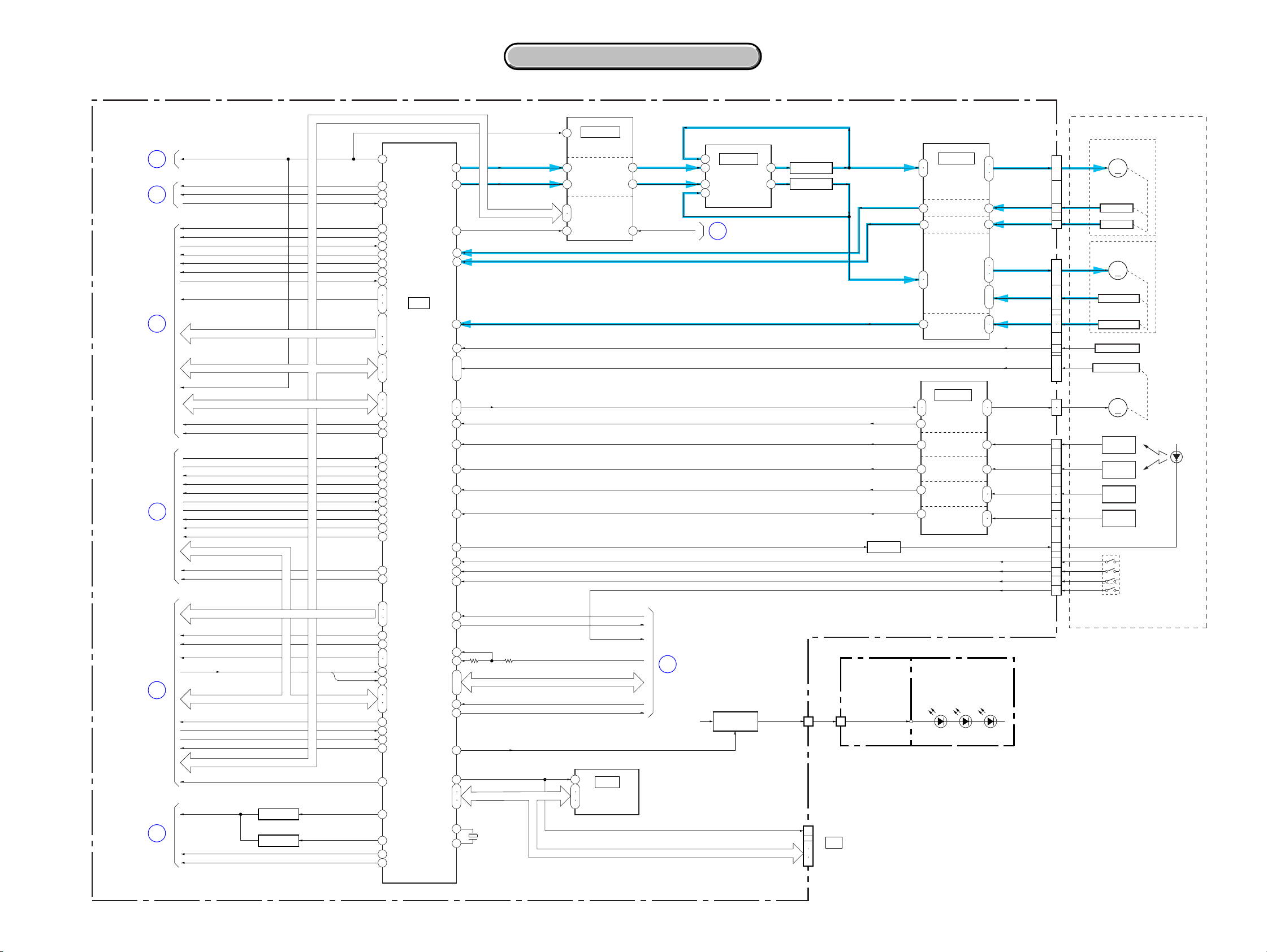
3-6. POWER BLOCK DIAGRAM (1/2)
VC-344 BOARD (1/2)
CN4001
6
5
1
4
2
3
05
Q4003, 4004
CHARGE
CONTROL
Q4001, 4002
CDET
36
VIN
43
VCC0
56
VCC1
55
DC CONTROL, RESET
VREF
37
DTC6
1
RT
30
DC IN
BT901
BATTERY
TERMINAL
+
S
–
+
–
BATT UNREG
BATT SIG
BATT GND
ACV UNREG
BATT/XEXT
ACV GND
( ) : Number in parenthesis ( ) indicates the division number of schematic diagram where the component is located.
BATT SIG
BATT/XEXT
INIT CHARGE ON
FAST CHARGE
VOUT
SEL
CS
VBAT
REG 3V
VRO
RST
LD
DIN
CLK
CTL1
IC1301
(9/10)
VR
OUT2
+INE2
OUT1
OUT3
IN3
OUT7
–INE7
OUT4
IN4
F002
D1306
Q1316, 1318, 1320
5V REG
L1311
L1310
L1319
L1317
L1318
L1320
Q1302, 1312, 1313
+15V REG
L1308
L1309
L1314
L1313
L1315
L1312
L1316
1
5
Q1301, 1303
13.5V REG
Q1304, 1314
–7.5V REG
IC1302
6V REG
(9/10)
Q1324, 1325
–15.3V REG
Q1315, 1317
1.9V REG
BL REG
4
F003
F004
BL REG UNREG
F001
VTR UNREG
42
32
44
39
40
41
29
26
27
28
38
34
58
21IN2
14
57
20IN1
59
22
63
2
60
23
D1301
Q1308
SWITCHING
BL CONT
D1302
Q1306
SWITCHING
Q1305
SWITCHING
Q1307
SWITCHING
L1301
L1304
L1302
L1305
L1303
Q1311
SWITCHING
D1303
D1305
FAST CHARGE
INIT CHARGE ON
BATT/XEXT
BATT SIG
BATT UNREG
MT 5V
VTR UNREG
V OUT
BATT IN
LI 3V
EVER 3.0V
XCS DD
HI EVER SO
HI EVER SCK
VTR DD ON
CAM DD ON
D 1.9V
D 1.5V
D 2.8V
A 2.8V
AU 2.8V
RP 2.8V
IN7 (VL 16V)
CAM –7.5V
CAM 15V
RP 6.0V
EP 4.6V
A 4.6V
AU 4.6V
RP 4.6V
EP 13.5V
CN1003
PANEL 2.8V
PANEL 4.6V
BL REG
PANEL –15.3V
PANEL 13.5V
BL CONT
A
POWER(2/2)
(PAGE 3-13)
17
18
2
16
19
4
TYPE C/S: Please refer to page 1-3 to descriminate the type of LCD.
PD- 204 BOARD
TYPE C
L6004
L6001
28
L6004
L6001
FB6001
IC6001
LCD DRIVER
FB6001
IC6001
LCD DRIVER
T6001, Q6002
INVERTER
TRANSFORMER
BACKLIGHT
DRIVE
18
16
19
17
4
2
BL REG
CN6001
PANEL 4.6V
PANEL –15.3V
PANEL 13.5V
PANEL 2.8V
BL CONT
TYPE S
PANEL 4.6V
PANEL –15.3V
PANEL 13.5V
PANEL 2.8V
BL CONT
L6002 L6003
R6026
R6019
R6020
Q6004, 6005,
6008, 6009
2428
BL HIGH
R6031
CN6004
VSH
VGL
VGH
VDD
VDD
CN6004
VSH5V
VGL
VGH
VSH3V
CN6003
LCD901
24
3
2.5INCH
1
COLOR
23
LCD UNIT
4
LCD901
24
3
2.5INCH
1
COLOR
23
LCD UNIT
ND901
10
BACK
LIGHT
3-11 3-12
3. BLOCK DIAGRAMS
3. BLOCK DIAGRAMS
DCR-TRV255E/TRV260/TRV265/TRV265E
3-7. POWER BLOCK DIAGRAM (2/2)
VC-344 BOARD (2/2)
BATT/XEXT
FAST CHARGE
INIT CHARGE ON
BATT SIG
BATT UNREG
MT 5V
VTR UNREG
VOUT
BATT IN
LI 3V
EVER 3.0V EVER 3.0V
XCS DD
HI EVER SO
HI EVER SCK
VTR DD ON
A
POWER (1/2)
(PAGE 3-12)
CAM DD ON
D 1.9V
D 1.5V
D 2.8V
A 2.8V
AU 2.8V
RP 2.8V
IN7 (VL 16V)
CAM –7.5V
CAM 15V
RP 6.0V
EP 4.6V
A 4.6V
AU 4.6V
RP 4.6V
EP 13.5V
L3203
FLYING
ERASE
OSC
Q3202, 3204, 3205
L3202
IC3201
REC/PB
(4/10)
AMP
L3201
FB2401
IC2401
LOADING/
DRUM/
CAPSTAN
MOTOR
DRIVE
(5/10)
VMR
VH
3
17
( ) : Number in parenthesis ( ) indicates the division number of schematic diagram where the component is located.
CHARGE LED VDD
BATT/XEXT
74
37
INIT CHARGE ON
38
35
20
21
33
56
IC3301
D/A CONVERTER,
LENS CONTROL,
STEADYSHOT
(2/10)
L3307
L3313
L3320
L3310
Q5408
AUDIO PROCESS
1
5
L3305
FB3303
IC5401
(8/10)
IC1001
3.3V REG
(10/10)
FB3301
4
D 2.8V
LI 3V
IC3302
DV
INTERFACE
(2/10)
IN7 (VL 16V)
CONVERTER
L3321
FB3302
IC5402
A/D, D/A
(8/10)
V LIGHT PWM
MODE LED VDD
CUSTOM LED VDD
USB 3.3V
Q1001
VIDEO
LIGHT
DRIVE
IN7 (VL 16V)
FB4501
CAM DD ON
173
CAMERA/MECHA
V LIGHT PWM
D 1.5V
D 1.9V
D 2.8V
A 2.8V
AU 2.8V
MT 5V
CAM –7.5V
CAM 15V
EP 4.6V
A 4.6V
AU 4.6V
IC4501
CONTROL
(6/10)
EVF DD ON
IC6501
Y/C MIX
BUFFER
(2/10)
L6501
91
173
55ZM RST LED
57FC RST LED
IC4502
EEPROM
(6/10)
Q5001
BATTERY
CHARGE
DETECTOR
S/H, AGC,
A/D CONVETER
43
42
54
55
31
IC1502 IC1501
(1/10)
FB1504
L1553
HALL BIAS/GAIN
Q1555
L1501
IC1552
IRIS DRIVE,
CONTROL,
HALL AMP
(3/10)
TIMING
GENERATOR
(1/10)
FB1501
IB SI
IB SO
BATT SENSE
ACV SENSE
BATT IN
IC5001
HI CONTROL
(7/10)
IC1601
EVR
(D/A CONVERTER)
(3/10)
FB1601
IC1554
XTAL AMP,
HALL REG
(3/10)
IC1553
FOCUS/ZOOM
MOTOR DRIVE
(3/10)
BATT/EXT
FAST CHARGE
INIT CHARGE
VTR DD ON
XCS DD 49
HI EVER SO
HI EVER SCK
XHI DS HELP
VTR DD SENSE
L1551
DV SIGNAL PROCESS,
CN1009
D 2.8V
CN1007
D 2.8V
D 2.8V
D 2.8V
LI 3V
CN1001
D 2.8V
MT 5V
CN1013
EVF DD ON
EP 4.6V
3.3V
CONTROL KEY BLOCK (SS-5100)
5
10
RV001
WT
11
(ZOOM)
CONTROL KEY BLOCK (CF-5100)
17
15
4
3
7
FUNCTION
SWITCH
D002
EASY
SI-041 BOARD
CN754
13
24
15
16
MT 5V
21
22
COMMANDER
FP-792 FLEXIBLE
LND754
VL+
1
36
EVF BLOCK
NSLEEP
2
EVF 4.6V
3
3.3V
1
LCD902
B/W
LCD
UNIT
D759
(TALLY)
TRV265/265E
IC751
REMOTE
RECEIVER
D001 – 003
(VIDEO LIGHT)
CAMERA
PLAY/EDIT
BT001
LITHIUM
BATTERY
(IR EMITTER)
D004
CHG
D002
D001
D753, 754
FG VCC
VH+
05
CAPSTAN
FG
17 8
CN2404CN2403
HE
SENSOR VCC
TAPE LED (A)
4 8
TAPE
LED
D001
T REEL,
S REEL,
SENSOR
H001,002
CN1551
FC SENSE
VCC
FOCUS
SENSOR
M2200 MECHA DECK
ZM SENSE
VCC
ZOOM
SENSOR
TEMP
SENSOR
LENS BLOCK
TEMP
18 241613
IRIS
METER
CD-471
BOARD
CAM 15V
1210
L951
IC951
CCD
IMAGER
CAM –7.5V
CN1501
35
CN951
IRIS DRIVE(+)
3-13 3-14E
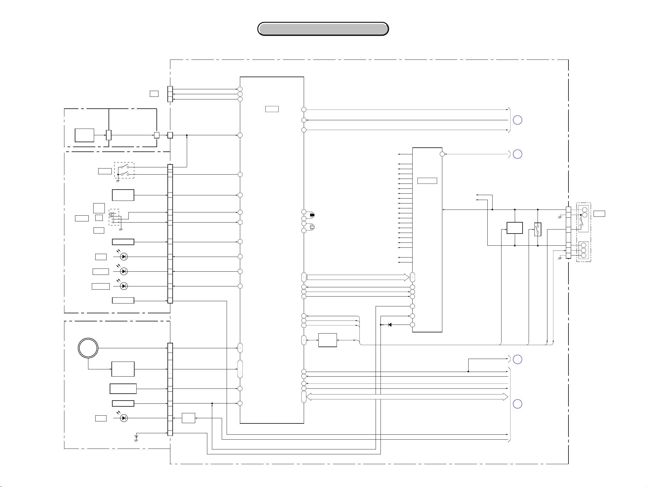
PRINTED WIRING BOARDS AND SCHEMATIC DIAGRAMS
4-1. FRAME SCHEMATIC DIAGRAMS
SECTION 4
4-2. SCHEMATIC DIAGRAMS 4-3. PRINTED WIRING BOARDS
4-2. SCHEMATIC DIAGRAMS 4-3. PRINTED WIRING BOARDS
DCR-TRV255E/TRV260/TRV265/TRV265E
1
FRAME SCHEMATIC DIAGRAM
A
2 10
B
LENS
C
D
E
FP-792
FLEXIBLE
MIC901
MICROPHONE
R
BOARD
F
VL+
REG_GND
REG_GND
LND757
LND754
G
LND763
H
4P
CN753
4
GND
GND
INT_MIC_R
SI-041
1 VCC
2D-
3D+
4ID
5GND
CN751
1NTPB
2 TPB
3NTPA
4 TPA
BOARD
5PCN752
4P
I
(USB)
J
TRV255E
DV
OUT
K
DV
TRV260
/TRV265/TRV265E
L
CONTROL
M
(PR-5100)
N
05
34 1814
CD-471
BOARDBLOCK
L
123
INT_MIC_L
24PCN1551
IRIS_HALL(+)
IRIS_DRIVE(+)
XF_TALLY_LED
XSIRCS_SIG
SIRCS_PWM/IR_DRV_EN
INT_MIC_R
IRIS_BIAS(+)
IRIS_HALL(-)
CN754
MIC_GND
MIC_GND
INT_MIC_L
VREF1
VREF2
A_2.8V
A_2.8V
D_2.8V
MT_5V
MT_5V
AV_JACK_IN
AUDIO_L_I/O
AUDIO_R_I/O
REG_GND
VIDEO_I/O
REG_GND
S_Y_I/O
XS_JACK_IN
S_C_I/O
REG_GND
REG_GND
REG_GND
USB_D-
USB_D+
USB_DET
IRIS_BIAS(-)
36P
VL+
LIA1
LIA2
NTPA
TPA
TPB
NTPB
TEMP
IRIS_DRIVE(-)
36
35
34
33
32
31
30
29
28
27
26
25
24
23
22
21
20
19
18
17
16
15
14
13
12
11
10
9
8
7
6
5
4
3
2
1
TEMP
KEY
BLOCK
5 12
CN951
14P
14
V4
13
V3
12
V2
11
V1
10
GND
9
H2
8
LENS_DET
ZM_SENSE_VCC
ZM_SENSE_OUT
FP-796 FLEXIBLE
6
5
4
3
2
1
FC_SENSE_VCC
FC_SENSE_OUT
CN1001
VL+
1
2
MIC_GND
MIC_GND
3
4
INT_MIC_L
5
INT_MIC_R
6
VREF1
LIA1
7
8
LIA2
VREF2
9
A_2.8V
10
A_2.8V
11
XF_TALLY_LED
12
D_2.8V
13
XSIRCS_SIG
14
MT_5V
15
MT_5V
16
SIRCS_PWM/IR_DRV_EN
17
AV_JACK_IN
18
AUDIO_L_I/O
19
AUDIO_R_I/O
20
REG_GND
21
VIDEO_I/O
22
REG_GND
23
S_Y_I/O
24
XS_JACK_IN
25
S_C_I/O
26
REG_GND
27
NTPA
28
TPA
29
REG_GND
30
TPB
31
NTPB
32
REG_GND
33
USB_D-
34
USB_D+
35
USB_DET
36
SE_GND
SE_GND
N.C.
N.C.
PANEL_REV
PANEL_REV
CAM_-7.5V
GND
CAM_15V
CCD_OUT
101112131415161718192021222324
ZOOM_A
36P
6PCN6005
GND
VSHT
GND
ZOOM_B
H1
RG
ZOOM_XB
7
6
5
4
3
2
1
ZOOM_XA
IR_SWITCH
FOCUS_A
IR_SWITCH
20P
CN1003
20P
CN6001
AD5
AD5
FOCUS_B
PANEL_13.5V
PANEL_13.5V
FFC-005
FLEXIBLE
FLAT CABLE
FOCUS_XB
PANEL_4.6V
PANEL_4.6V
123456789
FOCUS_XA
PANEL_2.8V
PANEL_2.8V
14PCN1501
CCD_OUT
PANEL_-15.3V
PANEL_-15.3V
GND
REG_GND
REG_GND
CAM_-7.5V
PANEL_HOLD
VD_SI(HDO)
VD_SI(HDO)
PANEL_HOLD
1011121314
VSHT
CAM_15V
(FOR CHECK)
VD_SO
VD_SCK
PD-124
HARNESS
VD_SO
VD_SCK
GND
CPC
XCS_LCD_DA
1011121314151617181920
1011121314151617181920
XCS_LCD_DA
PD-204
BOARD
When the machine needs to be repaired,please refer to
page 1-3 to discriminate the type of LCD(TYPE C or TYPE S).
C-SYNC/XHD
PANEL_XVD
9
8
8
9
PANEL_XVD
C-SYNC/XHD
H2RGH1
GND
16
15
14
13
12
11
10
9
8
7
6
5
4
3
2
1
PANEL_R
PANEL_R
16PCN1011
XCS_EEP
EEP_SI
EEP_SO
XLANC_PWR_ON
LANC_IN
LANC_OUT
REG_GND
PB_RF
REG_GND
REC_RF
REG_GND
SWP_DIR
CAP_FG
BPF_MONI
PB_RF
EEP_SCK
PANEL_G
PANEL_B
PANEL_B
PANEL_G
V3V1V2
BL_CONT
BL_CONT
BL_GND
BL_GND
123456789
V4
SE_GND
BL_REG
1234567
1234567
BL_REG
SE_GND
9
TAPE_TOP(C)
TAPE_LED(A)
TAPE_END(C)
S_REEL(-)
REG_GNDREG_GND
TAPE_LED(K)
123456789
15P
CN2404
TAPE_TOP(C)
S_REEL(-)
TAPE_LED(K)
TAPE_LED(A)
TAPE_END(C)
123456789
24P
VGL/VGL
VSS/GND
VGH/VGH
VDD/VGLAC
CN6004
N.C./SPS
S_REEL(+)
SENSOR_VCC
T_REEL(+)
T_REEL(-)
ME/MP
HALL_COM
HI8_MP
REC_PROOF
FP
1011121314
ME/MP
HI8_MP
T_REEL(-)
T_REEL(+)
S_REEL(+)
HALL_COM
SENSOR_VCC
REC_PROOF
VC-344 BOARD
LCD901
2.5INCH
COLOR
LCD UNIT
101112131415161718192021222324
GSRT/MO2
RESET/EX2
STBYB/PSG
VBC/CLS
VCOM/VCOM
GRES/EX1
GPCK/MO1
11 15
M2200 MECHANISM DECK
C_LOCK_SW
15
C_LOCK_SW
SRT/PSS1
STBYB/RES
22P
CN2403
DEW
DEW
OE/PSS2
M-SW(A)
M-SW(B)
M-SW(A)
M-SW(B)
CLR/CTR
MCLK/CLD
CN6004 Pin Name A/BNote:
A:
TYPE C MODEL
B: TYPE S MODEL
M-SW(C)
M-SW(C)
HCNT/SPD
FG VCC
FG1
FG1
FG VCC
VR/VR
VG/VG
CAP_W
CAP_W
CAP_U
REG_GND
CAP_U
CAP_V
FG2
FP
CAP_U
VSH/VSH5V
VDD/VSH3V
CAP_U
CAP_W
CAP_W
10111213141516171819202122
CAP_V
FG2
REG_GND
VB/VB
VSS/GND
13 17
CAP_V
CAP_V
HU1
HV1
HU2
HV2
VH+
HV1
HV2
VH+
HU2
HU1
ND901
BACKLIGHT
10
N.C
N.C
10PCN6003
BL_HIGH
FE(X)
VH-
HW1
HW2
123456789
11
11PCN3201
VH-
HW2
HW1
FE(X)
N.C
N.C
N.C
N.C
BL_LOW
4-1 4-2
1916678
20
21
EVF BLOCK
LCD902
B/W
LCD
UNIT
LM
SP2(X)
GND
FP
GND
XEVEN(SP2Y)
SP1(X)
SP1(Y)
YODD(SP1X)
XODD(SP1Y)
2PCN1008
SPEAKER
GND
GND
GND
123456789
GND
GND
GND
22PCN1007
SP(+)
SP(-)
1
2
SP901
U
V
V
U
W
W
FP
10
V
V
U
U
W
10P
CN2402
REG_GND
123456789
W
KEY_AD0
LI_3V
BATT_INFO
D_2.8V
CUSTOM_LED_VDD
N.C
COM
PG
FG
FG-PG_COM
1
2
123456789
2P
FG
PG
COM
FG-PG_COM
N.C
XCUSTOM_LED_ON
REG_GND
10111213141516171819202122
XMS_LED
N.C
LM(+)
CN2401
MS_LED_VDD
KEY_AD1
LM(-)
D_2.8V
KEY_AD3
D_2.8V
CN1009
XPOWER_SW
CHARGE_LED_VDD
XCHARGE_LED
MODE_LED_VDD
XPHOTO_FREEZE
ACV_UNREG
BATT_UNREG
KEY_AD2
DIAL_A
XS/S_SW
REG_GND
XMODE_SW
XCAM_LED
XVTR_LED
ZOOM_VR
REG_GND
KEY_AD5
XEJECT_SW
BATT_GND
BATT/XEXT
ACV_GND
BATT_SIG
DIAL_B
N.C
D_2.8V
REG_GND
16P
6PCN4001
XRESET
NC
NC
8PCN1013
13.3V
2NSLEEP
3EVF_4.6V
4HSYNC
5VSYNC
6VIDEO_IN
7DIG_GND
8ANA_GND
1
2
3
4
5
6
7
8
9
10
11
12
13
14
15
16
1
2
3
4
5
6
10
FP-797
FLEXIBLE
CONTROL
KEY
BLOCK
(SS-5100)
BT901
BATTERY
TERMINAL
3.3V3NSLEEP4EVF_4.6V5HSYNC6VSYNC7VIDEO_IN8DIG_GND9ANA_GND
1
2
GND
FE(Y)
SP2(Y)
10
GND
FE(Y)
YEVEN(SP2X)
CONTROL
KEY
123456789
LED
LED_GND
BLOCK
(CF-5100)
FRAME
Loading...