


 Loading...
PRODUCTION SWITCHER
DFS-800
4 DIGITAL VIDEO INPUT BOARD
BKDF-810
2 ANALOG VIDEO INPUT BOARD
BKDF-811
16 INPUT DME BOARD
BKDF-840
4 DIGITAL VIDEO OUTPUT BOARD
BKDF-860
2 ANALOG VIDEO OUTPUT BOARD
BKDF-861
SERVICE MANUAL 1st Edition
! WARNING
This manual is intended for qualified service personnel only.
To reduce the risk of electric shock, fire or injury, do not perform any servicing other than that contained in the operating instructions unless you are qualified to do so. Refer all servicing to qualified service personnel.
! WARNUNG
Die Anleitung ist nur für qualifiziertes Fachpersonal bestimmt.
Alle Wartungsarbeiten dürfen nur von qualifiziertem Fachpersonal ausgeführt werden. Um die Gefahr eines elektrischen Schlages, Feuergefahr und Verletzungen zu vermeiden, sind bei Wartungsarbeiten strikt die Angaben in der Anleitung zu befolgen. Andere als die angegeben Wartungsarbeiten dürfen nur von Personen ausgeführt werden, die eine spezielle Befähigung dazu besitzen.
! AVERTISSEMENT
Ce manual est destiné uniquement aux personnes compétentes en charge de l’entretien. Afin de réduire les risques de décharge électrique, d’incendie ou de blessure n’effectuer que les réparations indiquées dans le mode d’emploi à moins d’être qualifié pour en effectuer d’autres. Pour toute réparation faire appel à une personne compétente uniquement.
Attention-when the product is installed in Rack:
1.Prevention against overloading of branch circuit
When this product is installed in a rack and is supplied power from an outlet on the rack, please make sure that the rack does not overload the supply circuit.
2.Providing protective earth
When this product is installed in a rack and is supplied power from an outlet on the rack, please confirm that the outlet is provided with a suitable protective earth connection.
3.Internal air ambient temperature of the rack
When this product is installed in a rack, please make sure that the internal air ambient temperature of the rack is within the specified limit of this product.
For safety, do not connect the connector for peripheral device wiring that might have excessive voltage to the following port.
:TO CP connector
:TO MU connector
Follow the instructions for the above port.
4.Prevention against achieving hazardous condition due to uneven mechanical loading
When this product is installed in a rack, please make sure that the rack does not achieve hazardous condition due to uneven mechanical loading.
5.Install the equipment while taking the operating temperature of the equipment into consideration
For the operating temperature of the equipment, refer to the specifications of the Operation Manual.
6.When performing the installation, keep the following space away from walls in order to obtain proper exhaust and radiation of heat.
Front, Left : 10 cm (4 inches) or more
DFS-800
CAUTION
Danger of explosion if battery is incorrectly replaced.
Replace only with the same or equivalent type recommended by the manufacturer.
Dispose of used batteries according to the manufacturer’s instructions.
Vorsicht!
Explosionsgefahr bei unsachgemäßem Austausch der Batterie.
Ersatz nur durch denselben oder einen vom Hersteller empfohlenen ähnlichen Typ. Entsorgung gebrauchter Batterien nach Angaben des Herstellers.
ATTENTION
Il y a danger d’explosion s’il y a remplacement incorrect de la batterie.
Remplacer uniquement avec une batterie du même type ou d’un type équivalent recommandé par le constructeur.
Mettre au rebut les batteries usagées conformément aux instructions du fabricant.
DFS-800
ADVARSEL!
Lithiumbatteri-Eksplosionsfare ved fejlagtig håndtering.
Udskiftning må kun ske med batteri af samme fabrikat og type.
Levér det brugte batteri tilbage til leverandøren.
ADVARSEL
Lithiumbatteri - Eksplosjonsfare. Ved utskifting benyttes kun batteri som
anbefalt av apparatfabrikanten. Brukt batteri returneres apparatleverandøren.
VARNING
Explosionsfara vid felaktigt batteribyte. Använd samma batterityp eller en likvärdig typ som rekommenderas av apparattillverkaren. Kassera använt batteri enligt gällande föreskrifter.
VAROITUS
Paristo voi räjähtää jos se on virheellisesti asennettu.
Vaihda paristo ainoastaan laitevalmistajan suosittelemaan tyyppiin.
Hävitä käytetty paristo valmistajan ohjeiden mukaisesti.
1 (P)

Index
Before turning off the power ......................................................................................................................... |
1 |
1. Specification and Apperance ..................................................................................................................... |
2 |
1-1. Specification ...................................................................................................................................... |
2 |
1-1-1. DFS-800 Processor..................................................................................................................... |
2 |
1-1-2. DFS-800 Control Panel .............................................................................................................. |
3 |
1-1-3. BKDF-810.................................................................................................................................. |
4 |
1-1-4. BKDF-811 .................................................................................................................................. |
4 |
1-1-5. BKDF-860.................................................................................................................................. |
4 |
1-1-6. BKDF-861.................................................................................................................................. |
5 |
1-2. Appearance......................................................................................................................................... |
6 |
1-2-1. DFS-800 Processor..................................................................................................................... |
6 |
1-2-2. DFS-800 Control Panel .............................................................................................................. |
7 |
2. Name and Function of Each Block............................................................................................................ |
8 |
2-1. DFS-800 Processor ............................................................................................................................ |
8 |
2-2. DFS-800 Control Panel...................................................................................................................... |
9 |
2-2-1. Control Panel.............................................................................................................................. |
9 |
2-2-2. Rear Panel ................................................................................................................................ |
10 |
2-3. Peripheral Interface.......................................................................................................................... |
11 |
2-4. DFS-800 Board Configuration......................................................................................................... |
14 |
3. Connection............................................................................................................................................... |
15 |
3-1. Basic Configuration ......................................................................................................................... |
15 |
3-2. Option Configuration ....................................................................................................................... |
16 |
4. Function Block Diagram of Each Board ................................................................................................. |
17 |
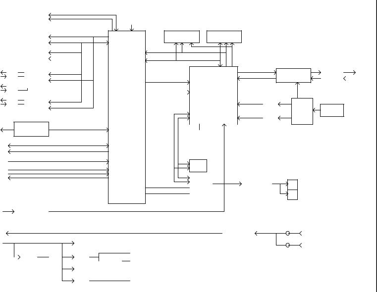
4-1. Function Block Diagram of CPU Board .......................................................................................... |
17 |
4-2. Function Block Diagram of MAIN Board ....................................................................................... |
18 |
4-3. Function Block Diagram of GENLOCK Board............................................................................... |
19 |
4-4. Function Block Diagram of BKDF-810 Board................................................................................ |
20 |
4-5. Function Block Diagram of BKDF-811 Board ................................................................................ |
21 |
4-6. Function Block Diagram of BKDF-840 Board................................................................................ |
22 |
4-7. Function Block Diagram of BKDF-860 Board................................................................................ |
23 |
4-8. Function Block Diagram of BKDF-861 Board................................................................................ |
24 |
5. Adjustment Procedure of Each Board...................................................................................................... |
25 |
5-1. Adjustment of CPU Board ............................................................................................................... |
25 |
5-2. Adjustment of MAIN Board ............................................................................................................ |
27 |
5-3. Adjustment of GENLOCK Board .................................................................................................... |
28 |
5-4. Adjustment of BKDF-810 Board ..................................................................................................... |
29 |
5-5. Adjustment of BKDF-811 Board ..................................................................................................... |
30 |
5-6. Adjustment of BKDF-840 Board ..................................................................................................... |
31 |
5-7. Adjustment of BKDF-860 Board ..................................................................................................... |
32 |
5-8. Adjustment of BKDF-861 Board ..................................................................................................... |
32 |
6. Method of Board Replacement/Addition................................................................................................. |
33 |
6-1. Removal/Installation of Shield Plate................................................................................................ |
33 |
6-1-1. Removal of Shield Plate ........................................................................................................... |
33 |
6-1-2. Installation of Shield Plate........................................................................................................ |
34 |
6-1-3. Caution on Insertion of Shield Plate......................................................................................... |
35 |
6-2. Replacement of CPU Board ............................................................................................................. |
36 |
6-2-1. Removal of CPU Board............................................................................................................ |
36 |
6-2-2. Installation of CPU Board ........................................................................................................ |
37 |
6-2-3. Setting....................................................................................................................................... |
37 |
6-3. Replacement of MAIN Board .......................................................................................................... |
38 |
6-3-1. Removal of MAIN Board......................................................................................................... |
38 |
6-3-2. Installation of MAIN Board ..................................................................................................... |
39 |
6-4. Replacement of GENLOCK Board.................................................................................................. |
40 |
6-4-1. Removal of GENLOCK Board................................................................................................. |
40 |
6-4-2. Installation of GENLOCK Board............................................................................................. |
41 |
6-5. Replacement/Addition of BKDF-810 Board.................................................................................... |
42 |
6-5-1. To Begin with ........................................................................................................................... |
42 |
6-5-2. Removal of BKDF-810 Board.................................................................................................. |
43 |
6-5-3. Installation of BKDF-810 Board .............................................................................................. |
44 |
6-5-4. Setting and Confirmation of Operation .................................................................................... |
45 |
6-6. Replacement/Addition of BKDF-811 .............................................................................................. |
46 |
6-6-1. To Begin with ........................................................................................................................... |
46 |
6-6-2. Removal of BKDF-811 Board.................................................................................................. |
47 |
6-6-3. Installation of BKDF-811 Board .............................................................................................. |
48 |
6-6-4. Setting and Confirmation of Operation .................................................................................... |
49 |
6-7. Replacement/Addition of BKDF-840 .............................................................................................. |
50 |
6-7-1. Removal of BKDF-840 Board.................................................................................................. |
50 |
6-7-2. Installation of BKDF-840 Board .............................................................................................. |
51 |
6-7-3. Setting and Confirmation of Operation .................................................................................... |
52 |
6-7-4. Positioning Drawing for affixing the rubber ............................................................................ |
52 |
6-8. Replacement/Addition of BKDF-860 Board.................................................................................... |
53 |
6-8-1. To Begin with ........................................................................................................................... |
53 |
6-8-2. Removal of BKDF-860 Board.................................................................................................. |
54 |
6-8-3. Installation of BKDF-860 Board .............................................................................................. |
55 |
6-8-4. Confirmation of Operation ....................................................................................................... |
55 |
6-9. Replacement/Addition of BKDF-861 Board.................................................................................... |
56 |
6-9-1. To Begin with ........................................................................................................................... |
56 |
6-9-2. Removal of BKDF-861 Board.................................................................................................. |
57 |
6-9-3. Installation of BKDF-861 Board .............................................................................................. |
58 |
6-9-4. Confirmation of Operation ....................................................................................................... |
59 |
7. Update of Firmware/Software ................................................................................................................. |
60 |
7-1. Procedure of Version Confirmation ................................................................................................. |
60 |
7-1-1. Confirmation of GUI Version................................................................................................... |
60 |
7-1-2. Confirmation of CPU1 Version ................................................................................................ |
60 |
7-2. Update Procedure............................................................................................................................. |
61 |
7-3. Update of GUI Software .................................................................................................................. |
62 |
7-4. Update of Board Firmware .............................................................................................................. |
62 |
8. FAQ Troubleshooting ........................................................................................................................... |
63 |
8-1. Trouble at Startup............................................................................................................................. |
63 |
8-2. Trouble related to Input and Output................................................................................................. |
64 |
8-3. Trouble after Board Addition/Replacement ..................................................................................... |
65 |
8-4. Trouble related to Updating ............................................................................................................. |
65 |
8-5. Trouble related to Function.............................................................................................................. |
66 |
9. Error Code Table ..................................................................................................................................... |
67 |
10. Replacement Parts for Mainteance ........................................................................................................ |
68 |
10-1. List of Replacement Parts for Maintenance ................................................................................... |
68 |
10-2. Replacement of DFS-800 Processor Parts ..................................................................................... |
69 |
10-2-1. Removal of Front Panel.......................................................................................................... |
69 |
10-2-2. Removal of Top Cover ........................................................................................................... |
69 |
10-2-3. Replacement of Power Unit ................................................................................................... |
70 |
10-2-4. Replacement of Fan................................................................................................................ |
74 |
10-3. Replacement of DFS-800 Control Panel Parts............................................................................... |
77 |
10-3-1. Removal of Control Panel ...................................................................................................... |
77 |
10-3-2. Replacement of Power Supply ............................................................................................... |
78 |
10-3-3. Replacement of Flash Memory .............................................................................................. |
80 |
10-3-4. Replacement of Button Cell ................................................................................................... |
81 |
Before turning off the power
Before turning off the DFS-800 Processor, shut down in the manner below.
1)Confirm that the USB is not accessed.
2)Press the F1 knob and F4 knob simultaneously. Then, the display on the panel changes as shown below.
Shutdown?
F2: OK F3: CANCEL
3)Press the F2 knob. ( To cancel the shutdow, press the F3 knob.)
4)When the F2 knpb is pressed, the shutdown begins. When the DFS-800 Processor is normally shut down, the display on the panel changes as shown below.
Shutdown…OK!
5)Turn off the power of Control Panel and then the power of Processor.
Before turning off the power, be sure to shut down. If the power is turned off before shut-down, the present panel setting cannot be saved. Therefore, the system is not
Caution normally terminated and the re-startup may fail.
When the system is normally shut down, the previous panel setting can be restored at the startup.
1

1. Specification and Apperance
1-1. Specification
1-1-1. DFS-800 Processor
Television System |
525/60, 625/50 |
|
Signal Process Method |
Digital Component 4:2:2 4 ( key ) 10 bits |
|
Quantization |
Y: 10 bits, C: 10 bits, Key: 10 bits |
|
Video Input |
SD SDI 270Mpbs, 75Ω, 8 inputs ( Expandable up to 16 inputs ), BNC |
|
Sync Signal Input |
BB: 0.429 Vp-p ( NTSC ) or 0.45 Vp-p ( PAL ), |
|
|
75Ω or loop-through, 1 input, BNC |
|
Video Output |
SD SDI 270Mpbs, 75Ω, 8 outputs ( Program 2 outputs, Preview, |
|
|
Clean 1 output each , Auxiliary 4 outputs ) ( Expandable up to 16 outputs ), |
|
|
BNC |
|
Sync Signal Output |
BB: 0.429 Vp-p ( NTSC ) or 0.45 Vp-p ( PAL ), 75Ω, 2 utputs, BNC |
|
I/O Delay |
1H (minimum delay) – 4 frames |
|
Interface |
|
|
TO OU |
Ethernet, 10/100BASE-TX, RJ-45; 1 port |
|
( To control panel ): |
|
|
RS-422: |
D-sub 9-pin ( female ), 2 ports |
|
EDITOR |
D-sub 9-pin ( female ), 1 port |
|
REMOTE: |
D-sub 37-pin ( female ), 1 port ( 8-pin input/24-pin output ) |
|
Operating Temperture |
5°C - 40°C |
|
Operating Humidity |
30% - 90% ( No dropwise ) |
|
Power Source |
100VAC-240VAC, 50/60Hz |
|
Current Consumption |
1.9A - 0.9A |
|
Maximun In-rush |
(1) Power ON, current probe method: 60A ( 240V ) |
|
Current |
(2) Hot switching inrush current, measured in accordance with European |
|
|
||
|
standard EN55103-1: 20A ( 230V ) |
|
Weight |
About 15kg |
|
Dimensions |
430 ( W ) x 425( D ) x 88 ( H ) mm, EIA 2RU |
|
Consumed Parts |
Cooling Fan: x1 at front side |
Replacement: every 4 years |
|
x2 at rear side |
Replacement: every 4 years |
2
1-1-2. DFS-800 Control Panel
USB |
USB1.1, A type ( female ), 1 port |
( Control Panel ) |
For USB memory stick ( Up to 2GB ). |
Interface |
|
TO PANEL |
D-sub 9-pin ( female ), 1 port |
TO MU (To switcher) |
Ethernet 10/100BASE-TX, RJ-45, 1 port |
VGA |
VGA OUT, D-sub 15-pin ( female ) |
USB: |
USB1.1, A type ( female ), 1 port |
Operating Temperature |
5°C - 40°C |
Operating Humidity |
30% - 90% ( No dropwise ) |
Power Source |
100VAC-240VAC, 50/60Hz |
Current Consumption |
0.5A - 0.2A |
Maximum In-rush |
(1) Power ON, current probe method: 40A ( 240V ) |
Current |
(2) Hot switching inrush current, measured in accordance with European |
|
|
|
standard EN55103-1: 10A ( 230V ) |
Weight |
About 5kg |
Dimenstions |
430 ( W ) x 221 ( D ) x 117 ( H ) mm |
3

1-1-3. BKDF-810
Television System |
525/60, 625/50 |
Video Input |
SD SDI 270Mpbs, 75Ω, 4 inputs, BNC |
I/O Delay |
1 Frame ( When FS is used ) |
1-1-4. BKDF-811
Television System |
525/60, 625/50 |
Video Input |
Analog Composite 2 inputs or |
|
Analog Composite and Analog Component 1 input each |
Analog Composite: 1.0V ( p-p ) 75Ω BNC
Analog Component
Y:1.0V ( p-p ) 75Ω BNC
B-Y, R-Y: 0.486V ( p-p ) ( SMPTE Level, 7.5% Setup )
0.525V ( p-p ) ( SMPTE Level, 0% Setup )
0.700V ( p-p ) ( Betacam Level, 7.5% Setup )
0.757V ( p-p ) ( Betacam Level, 0% Setup )
Phase Control |
±8 Pixcels |
I/O Delay |
1 Frame ( The FS is always turned on. ) |
1-1-5. BKDF-860
Television System |
525/60, 625/50 |
Video Input |
SD SDI 270Mpbs, 75Ω, 4 outputs, BNC |
4

1-1-6. BKDF-861
Television System |
525/60, 625/50 |
Video Output |
Analog Composite 2 outputs or |
|
Analog Composite and Analog Component 1 output each |
|
Analog Composite: 1.0V ( p-p ) 75Ω BNC |
Analog Component Y,B-Y,R-Y
Y:1.0V ( p-p ) 75Ω BNC
B-Y, R-Y: 0.486V ( p-p ) ( SMPTE Level, 7.5% Setup )
0.525V ( p-p ) ( SMPTE Level, 0% Setup )
0.700V ( p-p ) ( Betacam Level, 7.5% Setup )
0.757V ( p-p ) ( Betacam Level, 0% Setup )
Analog Component GBR
G, B, R: 1.0V ( p-p ) 75Ω BNC
Characterristics
At Analog Composite Output:
Frequency |
100kHz - 4.2MHz: ±0.5dB, |
Chatacteristics |
4.2MHz - 5MHz: within -1dB, |
|
Over 5MHz: Descending characteristics |
S/N Ratio |
60dB ( Excluding quantizing noise ) |
DG/DP |
1%/1° |
K Factor |
1% |
HV Tilt |
1% |
Residual Jitter |
±15ns |
At Analog Component Y,B-Y,R-Y output:
Frequency |
100kHz - 4.2MHz: ±0.5dB, |
Characteristics |
4.2MHz - 5MHz: within -1dB, |
|
Over 5MHz: Descending characteristics |
S/N Ratio |
60dB ( Excluding quantizing noise ) |
Linearity |
2% |
K Factor |
1% |
Phase difference |
10ns |
between Y/B-Y/R-Y |
|
At nalog Component GBR output:
Frequency |
100kHz - 5MHz: ±0.5dB, |
Chatacteristics |
Over 5MHz: Descending characteristics |
S/N Ratio |
60dB ( Excluding quantizing noise ) |
K Factor |
1% |
5

1-2. Appearance
1-2-1. DFS-800 Processor
( In mm. )
|
|
|
UO OT |
TUO BB |
NI KCOLNEG |
|
|
4 |
4 |
2 |
1 |
NI zH06/05 V042-001 CA |
|
|
|
|
|
|
|
3 |
3 |
|
|
|
|
2 |
2 |
|
|
ROTIDE |
2 |
1 |
|
|
|
|
224-SR |
ETOMER |
1 |
|
|
|
|
1 |
|
|
|
45
8 |
7 |
6 |
5 |
4 |
3 |
2 |
1 |
NI OEDIV |
4XUA |
3XUA |
2XUA |
1XUA |
NAELC |
VERP |
2MGP |
1MGP |
TUO OEDIV |
40
425
t2.3
|
6 |
88 |
76 |
|
6 |
2x2-6.4x12
345
7 |
|
|
|
24.5 |
|
|
40 |
|
|
|
|
26.5 |
16 |
56 |
16 |
|
DFS-800
PRODUCTION SWITCHER
ON
OFF
430
465
482
6

1-2-2. DFS-800 Control Panel
( In mm. )
7
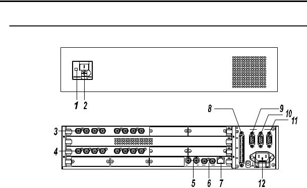
2. Name and Function of Each Block
2-1. DFS-800 Processor
Front Panel
ON |
OFF |
DFS-800
PRODUCTION SWITCHER
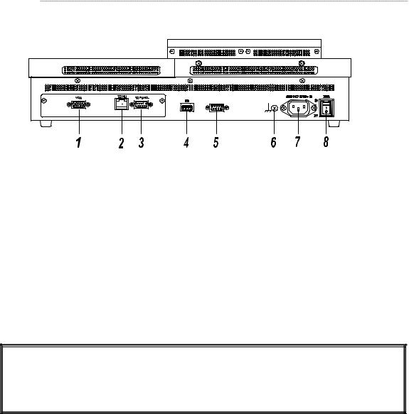
Rear Panel
VIDEO OUT |
PGM1 |
PGM2 |
PREV |
CL EAN |
AUX1 |
AUX2 |
AUX3 |
AUX4 |
VIDEO IN |
1 |
2 |
3 |
4 |
5 |
6 |
7 |
8 |
|
|
1 |
1 |
RS -422 |
|
|
|
|
REMOTE |
EDITOR |
|
|
|
|
1 |
2 |
|
|
|
2 |
2 |
|
|
|
|
3 |
3 |
|
|
|
|
|
|
AC 10 0-240 V 50/60Hz IN |
|
1 |
2 |
4 |
4 |
|
|
GENLOCK IN |
BB OUT |
TO OU |
|
|
|
|
No. |
|
|
Name |
|
Function |
|
1 |
|
POWER LAMP |
|
When turning on the power, the POWER lamp lights green. |
|||
2 |
|
POWER SWITCH |
|
Power switch of DFS-800 |
|
||
|
|
|
|
VIDEO OUT |
|
SD SDI Digital Video output |
|
|
3 |
|
|
|
2 programs, 1 preview, 1 clean and 4 auxiliaries are provided for |
||
|
|
|
|
|
|
standard output. 8 auxiliary outputs can be added. |
|
|
|
|
|
VIDEO INPUT |
|
SD SDI Digital Video output |
|
|
4 |
|
|
|
8 inputs are provided for standard input. 8 inputs can be added as |
||
|
|
|
|
|
|
an option. |
|
|
|
|
|
|
|
Connector for inputting the external sync signal ( black burst ) |
|
|
|
|
|
|
|
When a signal is fed to one connector, the other connector becomes |
|
|
5 |
|
|
GENLOCK IN |
|
automatically the loop through connector. |
|
|
|
|
|
|
|
When desiring no loop through, terminate the other connector with |
|
|
|
|
|
|
|
75Ω. |
|
6 |
|
REF OUT |
|
Connector for sync signal output 2 outputs |
|||
|
7 |
|
TO CP |
|
Connector for connecting the Control Panel ( RJ-45, |
||
|
|
|
10Base-T/100Base-TX ). |
|
|||
|
|
|
|
|
|
|
|
|
8 |
|
REMOTE |
|
Connector for inputting GPI, connector for outputting GPI/Tally |
||
|
|
|
D-sub 37-pin ( female ) |
|
|||
|
|
|
|
|
|
|
|
|
9 |
|
RS-422 -1 |
Connector for RS-422 control |
D-sub 9-pin ( female ) |
||
10 |
|
RS-422 -2 |
Connector for RS-422 control |
D-sub 9-pin ( female ) |
|||
11 |
|
|
RS-422 - EDITOR |
|
Connector for editor control |
D-sub 9-pin ( female ) |
|
|
12 |
|
AC IN |
For power input Feed AC100V - 240V. |
|||
8

2-2. DFS-800 Control Panel
2-2-1. Control Panel
The configuration of each part of control panel is as follows.
|
|
|
|
|
|
|
|
|
|
|
|
|
|
MENU |
|
|
EVENT |
|
|
|
|
|
|
|
|
|
|
|
|
|
|
|
|
|
|
|
|
|
|
|
7 |
8 |
9 |
- |
|
|
|
|
|
|
|
|
|
|
|
|
|
|
|
|
|
|
|
|
|
|
|
|
|
|
|
DEFAULT |
FINE |
|
X |
|
|
|
|
|
USBMEMORY |
|
|
|
|
|
|
|
|
|
|
|
|
|
SEQ |
|
|
STORE |
|
|
|
|
|
|
|
|
|
|
|
|
|
|
|
|
|
|
|
|
|
|
|
4 |
5 |
6 |
|
AUTO CK |
WIPE POS |
Y |
|
|
|
|
|
|
|
|
|
|
|
|
|
|
|
|
|
|
|
|
|
|
|
|
|
|
|
|
|
||||
|
|
|
|
|
|
|
|
|
|
|
|
|
|
|
LOOP |
DIR |
RECALL |
|
|
|
|
|
|
|
|
|
EDITOR |
|
|
|
|
|
|
|
|
|
|
|
|
|
1 |
2 |
3 |
|
DME POS |
DME ROT |
Z |
|
JOYSTICK |
|
|
|
|
|
|
|
|
|
|
|
|
|
|
|
|
|
|
|
|
|
|
|
|
|
|
|
|
|
|
|
|
|
|
|
|
|
|
|
|
|
|
|
|
|
|
NEW |
DELETE |
INSERT |
|
|
|
|
|
|
|
|
DFS-800 |
GPI |
|
|
|
|
|
|
|
|
|
|
|
|
|
0 |
. |
CANCEL |
ENTER |
|
|
|
|
|
|
PRODUCTION SWITCHER |
||
|
|
|
|
F1 |
|
F2 |
F3 |
|
F4 |
|
|
|
|
|
|
|
|
|
|
|
|
|||||
|
|
|
|
|
|
|
|
|
|
|
|
|
|
|
|
|
|
|
1 |
2 |
3 |
4 |
HIGH |
|
|
|
|
|
|
|
|
|
|
|
|
|
|
|
|
|
|
|
|
|
|
1 |
2 |
3 |
4 |
|
1 OVER 2 |
|
|
KEY ON |
EXT |
SELF |
CK |
MASK |
EDGESHADOW |
|
|
|
|
|
|
|
|
SEQ LINK |
FADER LIMIT |
NOR/REV |
REVERSE |
PREV TRANS |
1 |
2 |
3 |
4 |
|
PRIORITY |
||
|
|
KEYER |
|
|
|
|
|
|
PRODUCTIONSWITCHER |
|
|
|
FADER |
DIRECTION |
|
1 |
2 |
3 |
4 |
LOW |
1 |
2 |
|
|||
|
|
|
|
|
|
|
|
|
|
|
|
|
|
|
||||||||||||
|
|
|
|
|
|
|
|
|
|
|
|
|
|
|
|
|
|
|
|
KEYLAYER |
DSK |
|
||||
|
|
|
|
BUS SELECT |
|
|
|
|
|
|
DME |
|
|
|
|
|
|
|
|
|
|
|
KEY STATUS |
|||
|
|
|
|
|
|
|
|
|
|
|
|
|
|
|
|
|
|
|
|
|
|
|
|
|
||
KEY1 |
KEY2 |
KEY3 |
|
KEY4 |
DSK1 |
DSK2 |
COMBA |
COMBB |
BASIC |
BORDER |
SUB EFF |
WARP |
LIGHT |
SHIFT |
|
|
|
BKGD |
|
KEY |
|
|
KEY |
DSK |
|
|
MATTE |
INPUT |
AUX |
|
SYSTEM |
STATUS |
STILL |
SEQ |
EVENT |
|
|
|
|
|
|
|
|
|
|
|
1 |
|
|
2 |
|
1 |
|
|
|
|
|
SETUP |
|
|
|
|
|
|
|
|
|
|
|
|
|
|
|
|
|
|
|
|
|
|
|
|
|
|
|
|
|
|
|
|
|
|
|
|
|
|
|
|
|
|
KEY |
|
|
KEY |
DSK |
|
|
|
|
|
|
|
|
|
|
|
|
|
|
|
|
|
|
|
|
|
|
3 |
|
|
4 |
|
2 |
|
BLACK |
1 |
2 |
|
3 |
4 |
5 |
6 |
7 |
8 |
9 |
10 |
11 |
12 |
SHIFT |
|
|
|
|
|
|
|
|
|
|
|
|
|
|
|
|
|
|
|
|
|
|
|
|
|
|
|
|
|
|
MIX |
WIPE |
|
|
DME |
|
|
BLACK |
|
PROGRAM |
|
|
|
|
|
|
|
|
|
|
|
|
|
|
|
|
|
(FAM) |
|
|
(NAM) |
|
|
TRANS |
||
|
|
|
|
|
|
|
|
|
|
|
|
|
COMBINER SETUP |
|
|
|
|
TRANSITION TYPE |
|
|
|
|
|
|||
|
|
|
|
|
|
|
|
|
|
|
|
|
|
|
|
|
|
|
|
|
|
|
||||
BLACK |
1 |
2 |
|
3 |
4 |
5 |
6 |
7 |
8 |
9 |
10 |
11 |
12 |
SHIFT |
|
|
|
CUT |
|
AUTO |
|
|
DSK |
DSK |
||
|
|
|
|
|
|
|
CUT |
MIX |
||||||||||||||||||
PRESET |
|
|
|
|
|
|
|
|
|
|
|
|
|
|
|
|
|
|
|
|
|
TRANSITION |
|
|
||
|
No. |
|
|
Name |
|
Function |
|
1 |
|
|
Display panel and menu |
|
2 digits display panel for menu and control knpb for menu |
|
|
|
control |
|
setting |
|
|
|
|
|
|
||
|
|
|
|
|
|
Operation mode select button of menu, event and sequence |
|
2 |
|
|
Keypad and mode button |
|
Used for input/change of menu. |
|
|
|
|
Used for save/call of event. |
||
|
|
|
|
|
|
|
|
|
|
|
|
|
Used for save/replay of sequence. |
|
3 |
|
|
USB Memory |
|
Used for save/read of data. ( exclusive for USB flash memory, |
|
|
|
|
up to 2GB, USB 1.1 or 2.0 ) |
||
|
|
|
|
|
|
|
|
4 |
|
EDITOR button |
Used for ON/OFF editor control. |
||
5 |
|
GPI button |
Used for ON/OFF of GPI IN control. |
|||
|
6 |
|
|
Keyer section |
|
Used for keyer setup. ( Settings of keyer signal, type |
|
|
|
|
selection,mask, edge and shadow ) |
||
|
|
|
|
|
|
|
|
7 |
|
|
BUS SELECT SETUP |
|
Selects a bus and displays menu. |
|
|
|
|
DME section |
|
|
|
8 |
|
M/E bus |
|
Selects the background video. |
|
9 |
|
Joystick block |
Used for menu operation and auto chroma key setting. |
|||
10 |
|
Transition block |
Executes the transitions of background and key. |
|||
9
2-2-2. Rear Panel
The configuration of rear panel of control panel is as follows.
|
No. |
Name |
Function |
|
|
1 |
|
VGA |
Cconnect the LCD monitor. |
|
2 |
|
TO MU |
Connect the Processor. ( RJ-45, 10Base-T/100Base-TX, |
|
|
category5, cross cable ) |
||
|
|
|
|
|
|
3 |
|
TO PANEL |
Connect the touch panel LCD. |
|
|
( RS232C, D-sub 9-pin (female ) ) |
||
|
|
|
|
|
4 |
|
USB |
Connect the USB flash memory. ( Up to 2GB, USB 1.1 or 2.0 ) |
|
|
5 |
|
― |
Not used |
6 |
|
Ground |
For safety, connect it to the ground. |
|
|
7 |
|
AC IN |
Using the supplied power cord, supply the AC power. |
|
|
( AC100V-240V 50/60Hz ). |
||
|
|
|
|
|
8 |
|
Power Switch |
Power switch of control panel |
|
The USB port is exclusively for connecting the mouse or USB flash memory. Other
Caution USB drive equipment cannot be recognized. Insert the USB memory stick either in the USB memory drive on the control panel or USB memory drive on the rear panel.
Do not insert in both of them at the same time.
10
2-3. Peripheral Interface
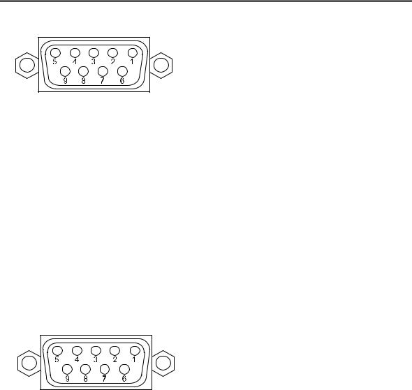
EDITOR CONNECTOR
Pin Assignment Table ( D-sub 9-pin, female )
Pin No. |
Signal Name |
Content |
1 |
FG |
Frame Ground |
2 |
T- |
Data Send ( - ) |
3 |
R+ |
Data Receive ( + ) |
4 |
SG |
Signal Ground |
5 |
- |
Not used |
6 |
SG |
Signal Ground |
7 |
T+ |
Data Send ( + ) |
8 |
R- |
Data Receive ( - ) |
9 |
FG |
Frame Ground |
|
|
|
Cable Connector: D-sub 9-pin connector ( male ), Inch screws are used.
RS-422 (1) (2) Connector
Pin Assignment Table ( D-sub 9-pin, female )
Pin No. |
Signal Name |
Content |
1 |
FG |
Frame Ground |
2 |
R- |
Data Receive ( - ) |
3 |
T+ |
Data Send ( + ) |
4 |
SG |
Signal Ground |
5 |
- |
Not used |
6 |
SG |
Signal Ground |
7 |
R+ |
Data Receive ( + ) |
8 |
T- |
Data Send ( - ) |
9 |
FG |
Frame Ground |
|
|
|
Cable Connector: D-sub 9-pin connector ( male ), Inch screws are used.
11
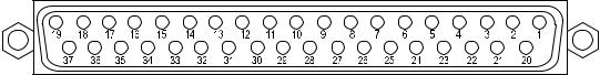
REMOTE Connector
Pin Assignment Table ( D-sub 37-pin, female )
Pin No. |
Pin Function |
Default Setting |
1 |
Tally Output 1 |
RedTallyInput01 |
2 |
Tally Output 2 |
RedTallyInput02 |
3 |
Tally Output 3 |
RedTallyInput03 |
4 |
Tally Output 4 |
RedTallyInput04 |
5 |
Tally Output 5 |
RedTallyInput05 |
6 |
Tally Output 6 |
RedTallyInput06 |
7 |
Tally Output 7 |
RedTallyInput07 |
8 |
Tally Output 8 |
RedTallyInput08 |
9 |
Tally Output 9 |
GreenTallyInput01 |
10 |
Tally Output 10 |
GreenTallyInput02 |
11 |
Tally Output 11 |
GreenTallyInput03 |
12 |
Tally Output 12 |
GreenTallyInput04 |
13 |
Tally Output 13 |
GreenTallyInput05 |
14 |
Tally Output 14 |
GreenTallyInput06 |
15 |
Tally Output 15 |
GreenTallyInput07 |
16 |
Tally Output 16 |
GreenTallyInput08 |
17 |
+5V |
|
18 |
+5V |
|
19 |
+5V |
|
20 |
Tally Output 17 |
None |
21 |
Tally Output 18 |
None |
22 |
Tally Output 19 |
None |
23 |
Tally Output 20 |
None |
24 |
Tally Output 21 |
None |
25 |
Tally Output 22 |
None |
26 |
Tally Output 23 |
None |
27 |
Tally Output 24 |
None |
28-29 |
GND |
|
30 |
GPI 1 |
PGMAutoTrans |
31 |
GPI 2 |
PGMCutTrans |
32 |
GPI 3 |
DSKAutoTrans< Mix > |
33 |
GPI 4 |
DSKCutTrans |
34 |
GPI 5 |
PGMMixType |
35 |
GPI 6 |
PGMWipeType |
36 |
GPI 7 |
PGMDMEType |
37 |
GPI 8 |
BlackTrans |
12
Cable Connector
D-sub 37-pin ( male ), Inch screws are used. Maximum load current DC 0.1A
Pin Free assignment
The table shown on the previous page shows the setting of pin assignment at ex-factory. They can be changed on the menu.
GPI Input Circuit
Switch or Relay |
|
|
Open Collector |
|
|
||||
|
|
|
|
|
|
|
|
|
|
External Equipment |
|
|
DFS-800 |
|
External Equipment |
|
|
DFS-800 |
|
|
VCC |
VCC |
|
VCC |
VCC |
||||
Tally Output Circuit
DFS-800 |
|
External Equipment |
||
|
|
|
|
|
|
|
Maximum voltage: |
||
|
|
30V |
||
|
Maximum load |
|||
|
current |
|||
|
100mA |
|
|
|
|
|
|||
13
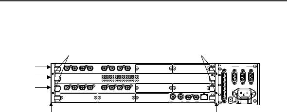
2-4. DFS-800 Board Configuration
The board configuration of DFS-800 rear panel is shown in the figure below and on the table. Each board is fixed with the retainer. To draw out the board from the unit, remove the retainers and then draw out the board.
Screw
1 |
VIDEO OUT |
PGM1 |
PGM2 |
PREV |
CL EAN |
AUX1 |
AUX2 |
AUX3 |
AUX4 |
2 |
|
|
|
|
|
|
|
|
|
3 |
VIDEO IN |
1 |
2 |
3 |
4 |
5 |
6 |
7 |
8 |
4 
Screw
1 |
1 |
RS -422 |
|
|
REMOTE |
|
|
|
1 |
2 |
EDITOR |
2 |
2 |
|
|
3 |
3 |
|
|
|
|
AC 10 0-240 V 50/60Hz IN |
|
1 |
2 |
4 |
4 |
GENLOCK IN |
BB OUT |
TO OU |
Retainer |
Retainer |
Configuration of Rear Panel Card of DFS-800 (From top slot to down slot)
Slot |
|
Standard/Option |
|
Card |
|
Content |
|||
1 |
|
Standard |
|
BKDF-860 |
Standard SD-SDI 1-8 Output |
||||
|
Option |
|
|
BKDF-860 / |
|
2 cards are expandable. ( *1 ) |
|
||
|
|
|
|
BKDF-861 |
|
|
|||
|
|
|
|
|
|
|
|
||
2 |
|
Standard |
|
MAIN |
|
MAIN card |
|||
|
Option |
|
|
BKDF-840 |
|
|
Input DME card |
||
|
|
|
|
|
|
( Pre-combiner ) |
|||
|
|
|
|
|
|
|
|
||
3 |
|
Standard |
|
BKDF-810 |
Standard SD-SDI 1-8 Input |
||||
|
Option |
|
|
BKDF-810 / |
|
2 cards are expandable. ( *1 ) |
|
||
|
|
|
|
BKDF-811 |
|
|
|||
|
|
|
|
|
|
|
|
||
4 |
|
Option |
|
|
BKDF-811 |
|
|
2 cards are expandable. ( *1 ) |
|
|
Standard |
|
CPU |
CPU card |
|||||
|
|
|
|||||||
*1 For expansion of option input, refer to [ 6-5. Replacement/Addition of BKDF-810 board ] and [ 6-6. Replacement/Addition of BKDF-811 board ]. For expansion of option output, refer to [ 6-8. Replacement/Addition of BKDF-860 board ] and [ 6-9.
Replacement/Addition of BKDF-861 board ].
14

3. Connection
3-1. Basic Configuration
TSG
VDA
Camera
Character
Generator
Digital Video
Database
GPI Controller
USB Flash Memory
|
|
|
Reference outputs |
(75ohm terminator) |
|
|
|
GENLOCK IN |
REF OUT |
|
|
(w/ loop-through |
|
|
|
1 |
|
PGM 1 |
PGM1 output |
IN 1 |
|
||
IN 2 |
|
PGM 2 |
PGM2 output |
IN 3 |
|
PREV |
PREV output |
IN 4 |
|
CLEAN |
|
|
CLEAN output |
||
IN 5 |
|
AUX1 |
|
IN 6 |
|
|
|
IN 7 |
|
AUX2 |
AUX outputs |
IN 8 |
|
AUX3 |
|
|
(Free assign) |
||
|
|
AUX4 |
|
DFS-800 Processor |
|
||
(30-37) REMOTE |
(1-27) |
Tally outputs |
|
EDITOR |
|
|
|
RS-422 1
RS-422 2
TO OU
Supplied LAN Cable
|
|
TO MU |
USB |
||
|
|
|
DFS-800ControlPanel

 Caution Connect to the Control Panel with the supplied control cable (10m) or ( LAN crosscable, category 5, RJ-45 ).
15

3-2. Option Configuration
TSG
VDA
Camera
Character
Generator 
Digital Video
Database
Analog Video
Database
GPI Controller
Editor, etc
|
|
|
|
|
|
|
|
|
|
|
Reference outputs |
|
|
|
|
(75ohm terminator) |
|
||||||
|
|
|
|
|
|||||||
|
|
|
GENLOCK IN |
|
REF OUT |
|
|
||||
|
|
(w/ loop-through |
|
|
|
|
|
PGM1 output |
|||
|
|
|
|
|
|
|
|||||
|
|
|
|
|
|
|
|
|
|
|
|
|
|
IN 1 |
|
|
|
PGM 1 |
|
||||
|
|
IN 2 |
|
|
|
REF OUT |
|
PGM2 output |
|||
|
|
|
|
|
PGM 2 |
|
|||||
|
|
IN 3 |
|
|
|
PREV |
|
PREV output |
|||
|
1 |
|
|
|
CLEAN |
|
CLEAN output |
||||
|
|
IN 4 |
|
|
|
|
|||||
|
|
IN 5 |
|
|
|
|
|
|
|
||
|
|
IN 6 |
|
|
|
AUX1 |
|
AUX outputs |
|||
|
|
IN 7 |
|
|
|
AUX2 |
|
||||
|
|
|
|
|
|
(SD-SDI) |
|||||
|
|
IN 8 |
|
|
|
AUX3 |
|
||||
|
|
|
|
|
|
|
|||||
|
|
IN 9 |
|
|
|
AUX4 |
|
|
|||
|
| |
|
|
|
AUX5 |
|
AUX outputs |
||||
|
|
IN 16 |
|
|
|
I |
|
||||
|
|
|
|
|
|
(Analog) |
|||||
|
|
|
|
|
|
|
|
AUX12 |
|
||
|
|
|
|
|
|
|
|
|
|||
|
|
|
|
|
|
|
|
|
|
||
|
|
|
|
|
|
|
|
|
|
|
|
DFS-800 Processor
BKDF-810
BKDF-811
BKDF-860
BKDF-861
BKDF-840
(30-37) REMOTE (1-27)  Tally outputs EDITOR
RS-422 1
RS-422 2
TO OU
Supplied LAN Cable
SVGA Display |
|
TO MU |
VGA |
DFS-800 |
|
USB Flash Memory |
USB |
Control Panel |
16
17
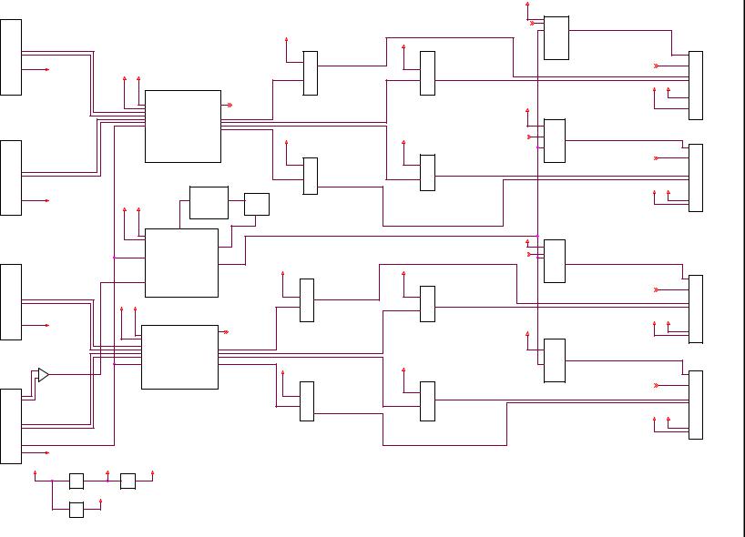
|
I2C |
DATA |
|
Dangle CD |
I2C |
CLK |
ConfigROM |
(I2C BUS EEPROM) |
|
|
XCF02S-VOG20 |
|
|
|
|
|
|
FLASH MEMORY |
|
Peripheral Address Bus 26bits |
|||
|
|
29LV128‚l |
|
Peripheral Data Bus 8bits |
|||
|
|
IC53 |
|
|
|
||
|
|
|
|
|
|
|
|
|
|
|
|
|
|||
|
FLASH MEMORY |
|
|
|
|||
|
29LV128‚l |
|
|
|
|||
|
IC57 |
|
|
|
|||
|
*NOT USED NOW |
|
|
|
|||
|
|
|
|
|
|
|
|
|
|
RS485 |
|
|
Serial I/F |
|
|
|
|
Driver |
|
|
Controller |
|
|
|
|
IC41 |
|
|
TL16C752B |
|
|
|
|
|
|
|
|
|
|
To Mother BD |
|
RS485 |
|
|
IC40 |
|
|
|
Driver |
|
|
|
|
|
|
|
|
|
|
||||
|
|
IC43 |
|
|
|
|
|
|
|
|
|
|
|
|
|
|
|
RS485 |
|
|
Serial I/F |
|
|
|
|
Driver |
|
|
Controller |
|
|
|
|
IC45 |
|
|
TL16C752B |
|
|
|
|
|
|
|
|
|
|
|
|
|
|
|
IC44 |
|
|
|
|
|
|
|
|
|
|
24bits
To Mother BD
To Mother BD
GPO
IC38,IC38,IC39,IC42 24bits ULN2003ANS
Transaction BUS 32bits
Transaction BUS Device select (Each FPGA has a CS)
Frame Pulse from Genlock CD
FAN ALARM 3bits
POWER ALARM 1bit
POWER LED CONTROL 2bits
8bits |
GPI |
8bits |
From Mother BD |
IC35,IC36 |
|
|
TLP280-4 |
|
|
|
|
FPGA Xilinx
XC2S300E-7FG456C
IC33
ADDRESS DECODER I2C I/F TARNSACTION BUS
SDRAM IC51 |
SDRAM IC52 |
EDS1232AATA |
EDS1232AATA |
133MHz |
133MHz |
133MHz |
Address Bus 22bits |
DATA Bus 64bits |
M2 Interface TX
|
|
|
M2 Interface RX |
|
Multiplexed intrrupt signal |
DSP IC3 |
|
||
|
TMS320DM642 |
|
||
Video intrrupt signal |
|
|
|
|
|
|
|
|
|
|
|
|
|
|
|
|
|
50MHz |
PLL |
|
|
|
|
IC19 |
I2C DATA |
|
|
|
ICS511M |
|
|
133MHz |
|
|
I2C CLK |
|
|
PLL |
|
|
|
|
|
IC19 |
|
|
|
|
ICS511M |
|
|
|
|
|
|
JTAG I/F |
|
|
|
|
DSP emulator |
|
|
|
|
|
|
|
|
EEPROM
IC24
24LC16B
|
ENCODER |
|
|
ENC_BB 16bits |
IC26 |
|
LEVEL & PEDESTAL |
|
IC28,IC62,IC27 |
||
|
ADV7176A |
|
|
H SYNC/FELED/BLANKING |
|
AD8091,AD8092 |
|
|
|
||
|
|
|
|
Ethernet Physical IC29
INTEL LXT971C
25MHz
25MHz
Clock Buffer
IC21
IDT5V2310
25MHz
BB OUT
CN1
BCJ-BPLH2P
IC30 |
|
|
PULSE TRANS |
|
RJ45 |
BEL FUSE |
|
|
|
|
|
Crystal
IC18
TQC73DCP
|
|
|
|
|
|
|
|
|
|
|
CN8 |
|
|
|
|
|
|
|
|
|
|
|
BCJ-BPLH2P |
|
Differential analog video signal go to the Genclock CD |
|
|
|
Differential Signal |
75 Ohme COAX CABLE |
|||||
To Mother BD |
|
|
|
|
|
|
|
Driver |
CN9 |
||
|
|
|
|
|
|
|
|
|
|
IC58,IC59 |
|
+5.25V |
|
|
|
|
|
+3.3V |
AD8132 |
BCJ-BPLH2P |
|||
From Mother BD |
|
IC46 |
|
|
|
|
|
|
75 Ohme COAX CABLE |
||
|
|
|
|
LP3966ES |
|
|
|
+2.5V |
|
|
|
|
|
|
|
|
|
|
|
|
|
||
|
|
|
|
|
|
|
|
|
|
||
|
|
P1 |
+1.8V |
IC48 |
|
|
|
|
|
|
|
|
|
AXH005AOX |
|
LP3966ES |
|
|
IC49 |
+1.4V |
|
|
|
|
|
|
|
|
|||||||
|
|
|
|
|
|
|
LP3965EMP |
|
|
|
|
|
|
|
|
|
|
|
|
|
|
|
|
|
|
|
|
IC50 |
|
|
|
+5.0V |
|
|
|
|
|
|
|
LT1764A |
|
|
|
|
|
|
|
|
|
|
|
|
|
|
-5.0V |
|
|
||
|
|
|
|
|
|
|
|
|
|
||
|
|
|
|
|
|
|
|
|
|
||
|
|
|
|
IC56 |
|
|
|
|
|
||
|
|
|
|
LM2660M |
|
|
|
|
|
|
|
|
|
|
|
|
|
|
|
|
|
|
|
of Diagram Block Function .1-4 |
of Diagram Block Function .4 |
Board CPU |
Board Each |
|
|

|
|
|
|
|
|
|
|
|
|
|
|
|
|
To Mother Board |
4 |
||
|
|
|
|
|
|
|
|
|
|
|
|
|
|
- |
|||
|
VIDEO IN(Slot1) |
|
VIDEO IN(Slot2) |
|
|
VIDEO IN(Slot3) |
|
VIDEO OUT(Slot1) |
VIDEO OUT(Slot3) |
VIDEO IN(Slot4) |
|
|
|||||
|
|
|
|
|
|
|
.2 |
||||||||||
|
|
|
|
|
LVDS 162MHz DDR |
LVDS 162MHz DDR |
LVDS 162MHz DDR |
|
|
||||||||
|
LVDS 162MHz DDR |
|
LVDS 162MHz DDR |
|
|
LVDS 162MHz DDR |
|
|
Transaction BUS |
||||||||
Transaction BUS |
|
Transaction BUS |
|
|
Transaction BUS |
Transaction BUS |
VIDEO OUT(Slot2) |
VIDEO OUT(Slot4) |
Pixel Clock 27MHz |
|
Clock IN 33MHz |
||||||
32bits 2.5V CMOS |
32bits 2.5V CMOS |
|
32bits 2.5V CMOS |
32bits 2.5V LVCMOS |
LVDS 162MHz DDR |
LVDS 162MHz DDR |
From Genlock CD |
|
|
Function |
|||||||
*Write Only* |
*Write Only* |
|
*Write Only* |
|
|
|
|
|
|
IC6 |
IC7 |
IC5 |
|||||
LVC16245 |
IC46IC45 |
|
IC49IC13 |
|
|
IC17IC14 |
|
LVC16245 IC18IC15 |
|
|
|
|
|||||
LVC16245 |
|
LVC16245 |
|
|
|
|
5V2310 |
5V2310 |
5V2310 |
|
|||||||
|
|
|
|
|
|
|
|
|
|
|
|
|
|
|
Transaction BUS |
|
|
|
|
|
|
|
|
|
|
|
|
|
|
|
|
|
Clock Distribution |
|
|
|
|
|
|
|
|
|
|
|
|
|
|
|
|
|
33MHz |
Block |
|
|
IC35 |
|
|
|
|
|
|
|
|
|
|
|
8ch Delay |
IC24 |
|||
|
IC38 |
|
|
|
|
|
|
|
|
|
|
|
IC26 |
|
|||
|
DVE ch1 |
|
|
|
|
|
IC30 |
|
|
|
Switcher Chip |
IC19 |
PGM/PRV/DSK1/DSK2 |
|
|||
|
DVE ch3 |
|
|
|
|
|
|
|
|
|
|
KEY1/KEY2/KEY3/KEY4 |
|
||||
|
|
|
|
|
|
|
|
|
|
M/E |
|
|
|
||||
|
|
|
|
Effects Chip |
|
|
|
|
|
|
|
|
|
|
|
||
|
IC36 |
|
|
|
|
|
|
KEYER |
|
|
|
|
IC25 |
|
|||
18 |
|
|
|
|
|
|
|
|
DSK |
|
|
6ch Trail Store |
Diagram |
||||
IC39 |
|
DVE Border |
|
|
|
|
|
|
|
IC27 |
|||||||
|
DVE ch2 |
|
|
|
|
|
|
|
Chromakey |
|
|
INPUT DVE Filed Delay |
|
||||
|
DVE ch5 |
|
|
Warp Engin |
|
|
|
|
|
WIPE Generator |
|
|
|
|
|
||
|
|
|
|
Lighting |
|
|
|
|
|
Mask Generator |
|
|
|
|
|
||
|
|
|
|
|
|
|
|
|
|
|
Edge Generator |
|
Still Store |
IC28 |
|
||
|
IC37 |
|
|
|
|
|
|
|
|
Still Store Controller |
|
|
|||||
|
|
|
|
|
|
|
|
|
|
IC29 |
|
||||||
|
IC40 |
|
|
|
|
|
|
|
|
Trail |
|
|
Caputure/Load |
|
|
||
|
DVE ch3 |
|
|
|
|
|
|
|
|
|
|
|
|
|
|||
|
DVE ch6 |
|
|
|
|
|
|
|
|
|
paint |
|
|
Key Delay for Edge |
|
||
|
|
|
|
|
|
|
|
|
|
|
Color Corrector |
|
|
|
|
|
|
|
|
|
|
|
|
|
|
|
|
|
SDRAM Controller |
|
|
|
|
of |
|
|
|
|
|
|
|
|
DC/DC |
P4 |
DC/DC |
P5 |
|
|
|
|
|
|
|
|
|
|
|
|
|
|
+5V to +1.5V |
+5V to +1.5V |
|
|
|
|
|
|
MAIN |
||
|
P2 |
|
|
|
|
|
CORE POWER |
|
CORE POWER |
|
|
|
|
|
|
|
|
|
|
|
|
|
|
|
|
|
|
|
|
|
|
|
|
||
|
DC/DC |
|
|
|
|
|
|
|
|
|
|
|
|
|
|
|
|
|
+5V to +3.3V |
|
|
|
|
|
|
|
|
|
|
|
|
|
|
|
|
|
I/O POWER |
|
|
|
|
|
|
|
|
|
|
|
|
|
|
|
|
|
P3 |
|
|
|
|
|
Cofiguration ROM |
Cofiguration ROM |
|
|
MAIN CD(E02886-1) |
|
|
||||
|
DC/DC |
|
|
|
|
|
|
|
|
|
|||||||
|
+5V to +2.5V |
|
|
|
|
|
IC33 |
|
IC22 |
|
|
|
|
|
|
|
|
|
I/O POWER |
|
|
|
|
|
|
|
|
|
|
|
|
|
|||
|
|
|
|
|
|
|
|
|
|
|
|
|
|
|
|
|
Board |
|
|
|
LVC16245 |
IC41 |
|
|
|
|
|
LVC16245 |
IC43 |
|
|
|
|
|
|
|
|
|
IC42 |
|
|
|
|
|
IC44 |
|
|
|
|
|
|
||
|
|
|
*Write Only* |
|
|
|
|
|
*Write Only* |
|
|
|
|
|
|
||
|
|
Transaction BUS |
|
VIDEO IN/OUT |
|
|
Transaction BUS |
VIDEO IN/OUT |
|
|
|
|
|
||||
|
|
32bits 2.5V LVCMOS |
LVDS 162MHz DDR |
|
|
32bits 2.5V LVCMOS |
LVDS 162MHz DDR |
|
|
|
|
|
|||||
|
|
|
DVE-SUB CD(E02882-1) |
|
|
DVE-SUB CD(E02882-1) |
|
|
|
|
|
||||||
|
To Mother Board |
|
|
|
|
|
|
|
|
CN1 |
|
|
|
|
|
|
|
|
|
|
|
|
|
|
3V.+3 |
IC7 |
|
|
|
|
|
|
|
|
|
|
VOD-A_N:4bit |
LVDS:162MHz |
|
|
|
|
DS90CR217 |
|
|
VOD-A_P:4bit |
LVDS:162MHz |
|
|
|
|
|
|
|
|
PS+5V |
|
5VD.+2 |
3VD.+3 |
|
VO0-A:10bit |
|
|
|
|
|
|
|
IC1 |
VO1-A:10bit |
|
|
|
|
|
|
|
|
|
|
|
|
|
|
|
|
XC3S400 |
|
|
|
|
|
|
|
|
|
CF_SYNC,LVDS_RST, |
|
|
|
|
|
|
|
|
FIFO_EN-AB,NCS, |
|
|
|
|
|
|
|
|
SCLK,SDIN |
|
|
CN2 |
|
|
|
|
|
3V.+3 |
IC9 |
|
|
|
|
|
|
|
|
DS90CR217 |
|
VOD-B_N:4bit |
LVDS:162MHz |
|
|
|
VO0-B:10bit |
|
|
|
|
|
|
|
|
|
|
|
|
VOD-B_P:4bit |
LVDS:162MHz |
|
|
|
VO1-B:10bit |
|
|
|
|
|
IC31 |
HD64F7045 |
|
|||
|
|
|
|
|
|
|
||
|
|
|
|
|
|
|
IC34 |
|
|
|
PS +5V |
|
5VD.+2 |
3VD.+3 |
|
|
|
|
|
|
|
|
|
IC29 |
|
|
|
|
|
|
|
|
EP1K100FC |
|
|
|
|
|
|
|
|
|
MH_SYNC,MF_SYNC,MV_SYNC |
|
19 |
CN3 |
|
|
|
|
|
3V.+3 |
|
|
|
|
|
|
|
IC14 |
||
|
|
|
|
|
|
|
|
DS90CR217 |
|
VOD-C_N:4bit LVDS:162MHz |
.+2 |
.+3 |
|
|
|
||
|
|
|
|
|
VO0-C:10bit |
|
||
|
VOD-C_P:4bit |
LVDS:162MHz |
5VD |
3VD |
|
|
||
|
|
|
|
|||||
|
|
|
|
|
|
IC4 |
|
|
|
|
+5V |
|
|
|
XC3S400 |
|
|
|
|
|
|
|
|
CF_SYNC,LVDS_RST, |
|
|
|
|
PS |
|
|
|
|
|
|
|
|
|
|
|
|
FIFO_EN-AB,NCS, |
|
|
|
|
|
|
|
|
|
|
|
|
|
|
|
|
|
|
SCLK,SDIN |
|
|
|
|
|
|
|
|
3V.+3 |
IC16 |
|
|
|
|
|
|
|
DS90CR217 |
|
|
CN4 |
|
|
|
|
|
|
|
|
|
|
|
|
|
|
VO0-D:10bit |
|
|
VOD-D_N:4bit |
LVDS:162MHz |
|
|
|
|
|
|
|
VOD-D_P:4bit |
LVDS:162MHz |
|
|
|
|
|
|
|
|
|
ADM:32bit |
|
|
|
|
|
|
PS+5V |
+5V |
|
3VD.+3 |
|
5VD.+2 |
|
|
|
PS |
P1 |
|
|
|
|||
|
|
|
IC42 |
|
|
|
|
|
|
|
|
AXH005AOX |
LP3965EMP |
|
|
|
|
|
|
|
P3 |
3.+3 |
|
|
|
|
|
|
|
SDI |
|
|
|
|
|
|
|
|
AXH005AOX |
|
|
|
|
|
|
|
|
|
|
|
|
|
|
3V.+3
VO2-A:10bit
VO3-A:10bit
3V.+3
VO2-B:10bit
VO3-B:10bit
3V.+3
VO2-A:10bit
VO3-A:10bit
3V.+3
VO2-B:10bit
VO3-B:10bit
3V.+3
CF_SYNC,LVDS_RST,
FIFO_EN-AB,NCS,
SCLK,SDIN
IC8
DS90CR217
3V.+3
|
CF_SYNC,LVDS_RST, |
|
IC10 |
FIFO_EN-AB,NCS, |
|
SCLK,SDIN |
||
DS90CR217 |
||
|
3V.+3
CF_SYNC,LVDS_RST,
FIFO_EN-AB,NCS,
SCLK,SDIN
IC15
DS90CR217
3V.+3
CF_SYNC,LVDS_RST, FIFO_EN-AB,NCS, 
IC17 SCLK,SDIN DS90CR217
IC11
LVCH16245 MH_SYNC-VA,MF_SYNC-VA,MV_SYNC-VA CF_SYNC-VA,LVDS_RST-RA,FIFO_RST-A FIFO_EN-A,NCS-A,SCLK-A,SDIN-A
|
|
CN7 |
|
DS0A_N:4bit |
IIC_CLK,IIC_DATA, |
|
|
PCB_ST |
|
||
DS0A_P:4bit |
|
||
PS +5V |
SDI 3.+3 |
||
DS1A_N:4bit |
|||
DS1A_P:4bit |
|||
|
|
||
IC12 |
|
|
|
LVCH16245 |
|
|
|
MH_SYNC-VA,MF_SYNC-VA,MV_SYNC-VA |
|||
CF_SYNC-VA,LVDS_RST-RA,FIFO_RST-A |
|||
FIFO_EN-A,NCS-A,SCLK-A,SDIN-A |
|||
|
|
CN8 |
|
IIC_CLK,IIC_DATA,
PCB_ST
DS1B_N:4bit
DS1B_P:4bit
DS0B_P:4bit |
PS+5V_ |
SDI_3.+3 |
DS0B_N:4bit |
|
|
IC18 |
|
|
|
LVCH16245 |
|
|
|
MH_SYNC-VA,MF_SYNC-VA,MV_SYNC-VA |
|||
CF_SYNC-VA,LVDS_RST-RA,FIFO_RST-A |
|||
FIFO_EN-A,NCS-A,SCLK-A,SDIN-A |
|||
|
|
CN9 |
|
|
IIC_CLK,IIC_DATA, |
|
|
DS0C_N:4bit |
PCB_ST |
|
|
DS0C_P:4bit |
|
|
|
DS1C_N:4bit |
PS+5V |
SDI3.+3 |
|
DS1C_P:4bit |
|||
IC19 |
|
|
|
LVCH16245 |
|
|
|
MH_SYNC-VA,MF_SYNC-VA,MV_SYNC-VA |
|||
CF_SYNC-VA,LVDS_RST-RA,FIFO_RST-A |
|||
FIFO_EN-A,NCS-A,SCLK-A,SDIN-A |
|||
|
|
CN10 |
|
|
IIC_CLK,IIC_DATA, |
|
|
DS1D_N:4bit PCB_ST |
|
||
DS1D_P:4bit |
|
|
|
DS0D_N:4bit |
PS+5V |
SDI3.+3 |
|
DS0D_P:4bit |
|||
|
|
||
Board GENLOCK of Diagram Block Function .3-4

20
|
|
|
SDI Input |
SDI INDEPENDENT CLOCK |
IC22, 23, 24, 25 = CLOCK BUFFER ( PI6CV304 ) |
FPGA |
|||||||
|
|
|
Equalizer |
QUAD DESERIALIZER |
IC6, 8, 9, 10 = DATA BUFFER ( 74LVCH16245 ) |
||||||||
|
|
|
( GS9064 ) |
( CYV15G0404RB ) |
|
|
|
|
( XC3S1500 ) |
||||
SDI Input A |
|
|
|
|
[VA-CLK] |
|
[VA-CLK2] |
|
|
[LVDS_DATA] |
|||
|
|
|
|
IC22 |
|
|
|
[LVDS_CLK] |
|||||
|
|
|
|
|
|
|
|
|
|
|
|||
|
|
|
|
IC1 |
[VA-EQ] |
|
|
|
|
|
|
IC11 |
|
|
|
|
|
|
|
|
|
[VA-DATA] |
|
[VA-DATA2] |
|
[LVDS_FRM] |
|
|
|
|
|
|
|
|
|
|
FUNCTION |
||||
|
|
|
|
|
|
|
|
|
|||||
|
|
|
|
|
|
|
|
|
IC6 |
||||
-VIDEO PROCESS ( BEFORE FRAME MEMORY )
>LUMINANCE GAIN
|
|
|
|
|
|
|
|
|
|
[VB-CLK2] |
|
|
> CHROMINANCE GAIN |
|
|
|
|
|
|
|
|
|
|
[ADM_CTRL] |
|
|
|
|
|
|
|
|
|
|||||
|
|
|
|
|
|
|
|
|
|
|
|
> LUMINANCE SETUP |
|
|
|
|
|
|
|
|
|
|
[ADM_DATA] |
|
|
|
|
|
|
|
|
|
||||||
|
SDI Input B |
|
|
|
[VB-CLK] |
IC23 |
|
|
|
|
> HUE CONTROL |
|
|
|
|
|
|
|
|
|
|
|
|
|
|
|
|
|
|
|
|
|
|
|||||
|
|
|
|
|
|
> WHITE CLIP |
|
|
|
|
|
|
|
|
|
|
|
|
|
|
|
|
|
|
|
|
|
|
||||||||||
|
|
|
|
|
IC2 |
[VB-EQ] |
|
|
|
|
|
> BLACK CLIP |
|
|
|
|
|
|
|
|
|
|
|
|
|
|
IC102 = CLOCK BUFFER ( 74LVC245 ) |
|
||||||||||
|
|
|
|
|
|
|
|
|
|
|
> CHROMINANCE CLIP |
|
|
|
|
|
|
|
|
|
|
|
|
|
|
|
|
|
|
|
|
|
||||||
|
|
|
|
|
|
|
|
[VB-DATA] |
|
[VB-DATA2] |
|
- LINE MEMORY ( USE MINIMUM DELAY MODE ONLY) |
|
|
|
|
|
|
|
|
|
|
|
|
[ADM_CLK] |
|
||||||||||||
|
|
|
|
|
|
|
|
IC8 |
|
- FRAME SYNCHRONIZER CONTROLER |
|
|
|
|
|
|
|
|
|
|
|
|
|
|
|
|
|
|||||||||||
|
|
|
|
|
|
|
|
|
|
|
- VIDEO FREEZE CONTROLER( FRAME , ODD , EVEN ) |
|
|
|
|
[ADM_CLK2] |
|
|
|
IC22 |
|
|
|
|
|
|||||||||||||
|
|
|
|
|
|
|
|
|
|
|
|
|
|
|
|
|
|
|
|
|
|
|
|
|
||||||||||||||
|
|
|
|
|
|
|
IC5 |
|
|
|
|
- AUTO VIDEO FREEZE CONTROLER |
|
|
|
|
|
|
|
|
|
|
|
|
|
|
|
|
|
|||||||||
|
|
|
|
|
|
|
|
[VC-CLK2] |
|
- STILL STORE CONTROLER |
|
|
|
|
|
|
|
|
|
|
|
|
|
|
|
|
|
|
|
|
||||||||
|
|
|
|
|
|
|
|
[VC-CLK] |
|
|
|
|
|
|
|
|
|
|
|
|
|
|
|
|
|
|
|
|
|
|
||||||||
|
|
|
|
|
|
|
|
|
|
|
|
|
|
|
|
|
|
|
|
|
|
|
|
|
|
|
|
|
|
|
|
|
|
|
|
|||
|
SDI Input C |
|
|
|
IC24 |
|
|
|
|
|
|
|
|
|
|
|
|
|
|
|
|
|
|
|
|
|
|
|
|
|
|
|
|
|
||||
|
|
|
|
|
IC3 |
[VC-EQ] |
|
[VC-DATA2] |
|
|
|
|
|
|
|
|
|
|
|
|
|
|
|
|
|
|
|
|
|
|
|
|
|
|
|
|||
|
|
|
|
|
|
|
[VC-DATA] |
|
|
|
|
|
|
|
|
|
|
|
|
|
|
|
|
|
|
|
|
|
|
|
|
|
|
|
|
|||
|
|
|
|
|
|
|
|
IC9 |
|
|
|
|
|
|
|
|
|
|
|
|
|
|
|
|
|
|
|
|
|
|
|
|
|
|
|
|||
|
|
|
|
|
|
|
|
[VD-CLK] |
[VD-CLK2] |
|
|
|
|
|
|
|
|
|
|
|
|
|
|
|
|
|
|
|
|
|
|
|
|
|
|
|
||
|
|
|
|
|
|
|
|
|
|
|
|
|
|
|
|
|
|
|
|
|
|
|
|
|
|
|
|
|
|
|
|
|
|
|
|
|||
|
|
|
|
|
|
|
|
|
|
|
|
|
|
|
|
|
|
|
|
|
|
|
|
|
|
|
|
|
|
|
|
|
|
|
|
|||
|
|
|
|
|
|
|
|
|
|
|
|
|
|
|
|
|
|
|
|
|
|
|
|
|
|
|
|
|
|
|
|
|
|
|
|
|||
|
|
|
|
|
|
|
|
IC25 |
|
|
|
|
|
|
|
|
|
|
|
|
|
|
|
|
|
|
|
|
|
|
|
|
|
|
|
|
|
|
|
SDI Input D |
|
[VD-EQ] |
|
|
|
|
|
|
|
|
|
|
|
|
|
|
|
|
|
[FVH] |
|
|
|
|
|
|
|
|
|
||||||||
|
|
|
|
|
IC4 |
|
|
[VD-DATA2] |
|
|
|
|
|
|
|
|
|
|
|
|
|
|
|
|
|
|
|
|
|
|
|
|
|
|
|
|||
|
|
|
|
|
|
|
[VD-DATA] |
IC10 |
|
|
|
|
|
|
|
|
|
|
|
|
|
|
|
|
|
|
|
|
|
|
|
|
|
|
|
|||
|
|
|
|
|
|
|
|
|
|
|
|
|
|
|
|
|
|
|
|
|
|
|
|
|
|
|
|
|
|
|
|
|
|
|
||||
|
|
|
|
|
|
|
|
|
|
|
|
|
|
|
|
|
|
|
|
|
|
|
|
|
|
|
|
|
|
|
|
|
|
|
|
|
||
|
|
|
|
|
|
|
|
|
|
|
|
|
|
|
|
|
|
|
|
|
|
|
|
|
|
|
|
|
|
|
|
|
|
|
|
|
|
|
|
|
|
|
|
|
|
|
|
|
|
[VA-DATA3] |
[VA-WCTRL] |
[VSA-DATA] |
[VSA-RCTRL] |
[VB-DATA3] |
[VB-WCTRL] |
[VSB-DATA] |
[VSB-RCTRL] |
[VC-DATA3] |
[VC-WCTRL] |
[VSC-DATA] |
[VSC-RCTRL] |
[VD-DATA3] |
[VD-WCTRL] |
[VSD-DATA] |
[VSD-RCTRL] |
|
|
|
|
|
|
|
|
|
|||
|
|
|
|
|
|
|
|
|
|
|
|
|
|
|
|
|
|
|
|
|
|
|
|
|
|
|
|
|
|
|
|
|
|
|
|
|
|
|
"*" is video channel name [ A, B, C, D ] |
|
|
|
|
IC27 |
|
|
|
|
|
|
|
|
|
|
|
|
|
|
|
|
|
|
|
|
|
|
|
|
|
||||||||
|
|
|
|
|
|
|
|
|
|
|
|
|
|
|
|
|
|
|
|
|
|
|
|
|
|
|
|
|
|
|||||||||
[V*-EQ] |
= 270MHz DIFFERENTIAL (Equalizer out) |
|
|
|
|
FRAME |
|
|
|
|
|
|
|
|
|
|
|
|
|
|
|
|
|
|
|
|
|
|
|
|
|
|||||||
[V*-CLK] |
= 27MHz PIX_CLK |
|
|
|
|
FIFO |
|
|
|
|
|
|
|
|
|
|
|
|
|
|
|
|
|
|
|
|
|
|
|
|
|
|||||||
|
[VA-CLK2] |
|
|
MEMORY |
|
|
|
|
|
|
|
|
|
|
|
|
|
|
|
|
|
|
|
|
|
|
|
|
|
|||||||||
[V*-CLK2] |
= 27MHz BUFFERED PIX_CLK [ delayed 1-3ns ] |
|
|
|
|
|
|
|
|
|
|
|
|
|
|
|
|
|
|
|
|
|
|
|
|
|
|
|
|
|||||||||
|
|
|
|
|
|
|
|
|
|
|
|
|
|
|
|
|
|
|
|
|
|
[ADM_CLK2] |
|
|||||||||||||||
[V*-DATA] |
= 27MHz 10BIT SCRAMBLE VIDEO DATA (synchronus PIX_CLK) |
|
|
|
|
|
|
|
|
|
|
|
|
|
|
|
|
|
|
|
[CONFIG] |
|
|
|
|
|
|
|
|
|
|
|||||||
[V*-DATA2] |
= BUFFERED 27MHz 10BIT SCRAMBLE VIDEO DATA (synchronus PIX_CLK) |
|
|
|
|
|
|
|
IC29 |
|
|
|
|
|
|
|
|
|
|
|
|
IC14, 15, 101 |
[ADM_CTRL] |
|
||||||||||||||
|
|
[ delayed 1-4ns ] |
|
|
|
|
|
|
|
|
|
|
|
|
|
|
|
|
|
|
|
|
CONFIG ROM |
|
|
|
|
|
|
|
|
|||||||
|
|
|
|
|
|
|
|
|
|
|
|
|
|
|
|
|
|
|
|
|
|
|
|
|
|
|
|
|
|
|||||||||
[V*-DATA3] |
= 27MHz 10BIT DESCRAMBLE VIDEO DATA (synchronus PIX_CLK) |
|
|
|
|
|
|
|
FRAME |
|
|
|
|
|
|
|
|
|
|
|
|
|
[JTAG_IN] |
|||||||||||||||
[V*-WCTRL] |
= 4BIT FRAME MEMORY WRITE CONTROL DATA (synchronus PIX_CLK) |
|
|
|
|
|
|
|
FIFO |
|
|
|
|
|
|
|
|
|
|
|
|
|
|
[JTAG_OUT] |
||||||||||||||
|
[VB-CLK2] |
|
|
|
|
MEMORY |
|
|
|
|
|
|
|
|
|
|
|
|
|
|||||||||||||||||||
|
|
|
|
|
|
|
|
|
|
|
|
|
|
|
|
|
|
|
|
|
|
|
|
|
|
|
||||||||||||
[VS*-DATA] |
= 27MHz 10BIT DESCRAMBLE VIDEO DATA (synchronus SYS_CLK) |
|
|
|
|
|
|
|
|
|
|
|
|
|
|
|
|
|
|
|
|
|
|
|
|
|
|
|
|
|
|
|||||||
[VS*-RCTRL] |
= 4BIT FRAME MEMORY READ CONTROL DATA (synchronus SYS_CLK) |
|
|
|
|
|
|
|
|
|
|
|
IC28 |
|
|
|
|
|
|
|
|
|
|
|
|
|
|
|
|
|
|
|||||||
[LVDS_DATA] = 162MHz DDR 5 pair video data 162MHZ1 pair clock + 1 pair frame |
|
|
|
|
|
|
|
|
|
|
|
FRAME |
|
|
|
|
|
|
|
|
|
|
|
|
|
|
|
|
|
|||||||||
|
|
|
|
|
|
|
|
|
|
|
|
|
|
|
|
|
|
|
|
|
|
|
|
|
|
|
|
|||||||||||
[LVDS_CLK] |
= 162MHz 1 pair clock |
|
|
|
|
|
|
|
|
|
|
|
|
|
|
|
|
|
|
|
|
|
|
|
|
|
|
|
|
|||||||||
|
[VC-CLK2] |
|
|
|
|
|
|
|
|
FIFO |
|
|
|
|
|
|
|
|
|
|
|
|
|
|
|
|
|
|
||||||||||
[LVDS_FRM] |
= 162MHz 1 pair frame |
|
|
|
|
|
|
|
|
|
MEMORY |
|
|
|
|
|
|
|
|
|
|
|
|
|
|
|
|
|
||||||||||
[FVH] |
= field pulse + vertical pulse + horizontal pulse |
|
|
|
|
|
|
|
|
|
|
|
|
|
|
|
|
|
|
|
[SYS_CLK2] |
|
|
|
[SYS_CLK] |
|||||||||||||
[SYS_CLK] |
= 27MHz SYSTEM CLOCK |
|
|
|
|
|
|
|
|
|
|
|
|
|
|
|
|
IC30 |
|
|
[SYS_CLK2] |
IC16, |
17, 18, 19, 20, 21 |
|
|
|
|
|
|
|
||||||||
[DBG_CLK] |
= 27MHz CLOCK ( DEBUG CLOCK ) |
|
|
|
|
|
|
|
|
|
|
|
|
|
|
|
|
|
|
[SYS_CLK2] |
|
|
|
|
|
|
|
|||||||||||
|
|
|
|
|
|
|
|
|
|
|
|
|
|
|
|
|
|
|
SYSTEM CLOCK DRIVERS |
|
|
|
|
|
|
|
||||||||||||
[SYS_CLK2] |
= 27MHz SYSTEM CLOCK [ delayed 2.335 - 4.91ns ] |
|
|
|
|
|
|
|
|
|
|
|
|
|
|
|
|
FRAME |
|
[SYS_CLK2] |
|
|
|
|
|
|
|
|||||||||||
|
|
|
|
|
|
|
|
|
|
|
|
|
|
|
|
|
|
|
|
|
|
|
|
|
|
|
||||||||||||
[SYS_CLK_D] |
= 27MHz DIFFERENTIAL SYSTEM CLOCK [ delayed 0.87 - 1.695ns ] |
|
|
|
|
|
|
|
|
|
|
|
|
|
|
|
|
FIFO |
|
|
[SYS_CLK2] |
|
|
|
|
|
|
|
|
|
|
|||||||
|
[VD-CLK2] |
|
|
|
|
|
|
|
|
|
|
|
|
|
MEMORY |
|
|
|
|
|
|
|
|
|
|
|
||||||||||||
[ADM_CLK] |
|
|
|
|
|
|
|
|
|
|
|
|
|
|
|
|
|
|
|
|
|
|
|
|
|
|
|
[DBG_CLK] |
|
|
|
|||||||
= 33MHz CPU_DATA_CLK |
|
|
|
|
|
|
|
|
|
|
|
|
|
|
|
|
|
|
|
[SYS_CLK_D] |
|
|
|
X2 |
|
|
||||||||||||
|
|
|
|
|
|
|
|
|
|
|
|
|
|
|
|
|
|
|
|
|
|
|
|
|
|
|
|
|||||||||||
[ADM_CLK2] |
= 33MHz CPU_DATA_CLK [ delayed 16ns ] |
|
|
|
|
|
|
|
|
|
|
|
|
|
|
|
|
|
|
|
|
|
|
|
|
|
|
|
|
|
|
|||||||
[ADM_DATA] |
= 33MHz CPU_DATA |
|
|
|
|
|
|
|
|
|
|
|
|
|
|
|
|
|
|
|
|
|
|
|
|
|
|
|
|
|
|
|||||||
|
|
|
|
|
|
|
|
|
|
|
|
|
|
|
|
|
|
|
|
|
|
|
|
|
|
|
|
|
|
|||||||||
[ADM_CTRL] |
= CPU_CHIPSELECT & CPU_READY |
|
|
|
|
|
|
|
|
|
|
|
|
|
|
|
|
|
|
|
|
|
|
|
|
|
|
|
|
|
|
|||||||
[CONFIG] |
= FPGA CONFIG DATA |
|
|
|
|
|
|
|
|
|
|
|
|
|
|
|
|
|
|
|
|
|
|
|
|
|
|
|
|
|
|
|||||||
[JTAG_IN] |
= JTAG TDI & TMS FOR CPU WRITE CONFIG ROM |
|
|
|
|
|
|
|
|
|
|
|
|
|
|
|
|
|
|
|
|
|
|
|
|
|
|
|
|
|
|
|||||||
[JTAG_OUT] |
= JTAG TDO FOR CPU WRITE CONFIG ROM |
|
|
|
|
|
|
|
|
|
|
|
|
|
|
|
|
|
|
|
|
|
|
|
|
|
|
|
|
|
|
|||||||
CONNECTOR ( 8071 )
CN8
Board 810-BKDF of Diagram Block Function .4-4

4-5. Function Block Diagram of BKDF-811 Board
CN8
|
LVDS,162MHz |
5pair |
DSP DATA:32bit |
SYSYEM CLK |
|
|
|
|
|
|
|
|
|
|
|
VCC0 VCCAUX,VCC0 VCCINT |
FPGA |
IC11 |
XC3S1500-4FGG456C |
|
|
|
|
SDA,SCLK |
|
|
|
|
|
|
+3.3V |
|
|
|
|
|
|
|
|
|
|
|
|
|
|
+2.5V |
|
|
|
|
|
|
|
|
|
|
|
|
|
|
+1.2V_core |
|
|
|
|
|
|
|
|
|
|
|
|
|
|
|
VA FM RD:10bit |
VA FM WD:10bit |
S CLK |
|
VB FM RD:10bit |
VB FM WD:10bit |
S CLK |
|
|
|
|
|
|
|
IC27 |
MS81V26000-12TB |
|
CH1 |
|
|
|
CH2 |
IC28 |
MS81V26000-12TB |
|
|
|
|
|
+3.3V |
|
FMVACLK |
|
+3.3V |
|
FMVBCLK |
|
BUS |
|
|
|
|
|
|
|
|
|
|
|
|
|
|
|
I2C |
|
|
|
|
|
DV 1:10bit |
|
|
|
DV 2:10it |
|
|
|
|
|
|
|
|
|
|
DECORDER1 |
SDA,SCLK |
|
|
DECORDER2 |
SDA,SCLK |
|
|
|
|
|
|
|
|
+1.8V |
|
ADV7189 |
+1.8V |
|
ADV7189 |
|
|
|
+2.5V |
+1.8VA |
+1.8VD |
|
||
+3.3V |
|
|
|
+3.3V |
|
|
|
|
|
|
|
|
|
|
|
Filter |
|
Filter |
|
Filter |
|
|
Filter |
|
+5.0VA |
+3.3VA |
+3.3VD |
+1.2VCORE |
-5.0VA |
|
InputAmp |
|
InputAmp |
-5V |
InputAmp |
-5V |
|
InputAmp |
-5V |
+5.2V |
|
|
|
|
|
-5V |
|
|
|
|
|
|
|
|
|
||||
+5V |
+5V |
|
|
+5V |
|
+5V |
|
|
|
|
|
|
|
|
|
|
|
|
|
|
|
|
|
|
|
||||
|
|
|
|
|
|
21 |
|
|
|
|
|
|
|
|

|
|
|
|
|
|
|
|
To Main Card |
.6-4 |
|
JTAG CHAIN |
VIDEO OUT 4ch |
VIDEO IN 17ch |
Transaction BUS |
|
|
+5V |
||
|
for update FGPA data |
LVDS 162MHz DDR |
LVDS 162MHz DDR |
32bits 2.5V LVCMOS |
|
|
Function |
||
|
|
|
|
|
*Write Only* |
|
|
|
|
REG |
IC21 |
Cofiguration ROM |
|
|
|
|
|
|
|
3.3V to 1.8V |
|
|
|
|
|
|
|
||
XCF16VOG48 |
|
|
|
|
|
|
|
||
|
|
|
|
|
|
|
|
|
|
to XCF16( IC4 ) |
IC4 |
|
|
|
|
|
|
|
|
|
|
|
|
|
|
|
Block |
||
|
Synchronous SRAM |
|
|
|
|
|
|
||
|
CY7C1372D |
|
|
|
|
|
|
|
|
22 |
|
|
|
|
|
|
DC/DC P2 |
Diagram |
|
IC18 & IC20 |
|
Input DVE 16ch & Pre-Combiner |
|
AXH005AOX |
|||||
|
|
|
XC2VP30-5FF1152 |
|
|
+5V to +2.5V |
|
||
|
|
|
IC1 |
|
|
|
I/O POWER |
|
|
|
|
|
|
|
|
|
(XILINX LVDS & |
|
|
|
Synchronous SRAM |
|
|
|
Synchronous SRAM |
Configuration) |
|
||
|
|
|
|
|
|
|
|||
|
CY7C1372D |
|
|
|
|
CY7C1372D |
|
|
|
|
|
|
|
|
|
|
DC/DC |
P5 |
|
|
|
|
|
|
|
|
BSV-H |
|
|
|
|
|
|
|
|
|
+5V to +3.3V |
of |
|
|
IC17 & IC19 |
|
|
|
|
IC5 & IC7 |
I/O & SRAM POWER |
||
|
|
|
|
|
|
||||
|
Synchronous SRAM |
|
|
|
Synchronous SRAM |
DC/DC |
P4 |
-BKDF |
|
|
CY7C1372D |
|
|
|
|
CY7C1372D |
|
||
|
|
|
|
|
BSV-H |
|
|
||
|
|
|
|
|
|
|
|
|
|
|
|
|
|
|
|
|
+5V to +1.5V |
|
|
|
|
|
|
|
|
|
CORE POWER |
|
|
|
IC14 & IC16 |
|
|
|
|
IC6 & IC8 |
|
|
840 |
|
|
|
|
|
|
|
|
|
|
|
|
Synchronous SRAM |
Synchronous SRAM |
Synchronous SRAM |
|
|
|
Board |
|
|
|
CY7C1372D |
|
CY7C1372D |
CY7C1372D |
|
|
|
|
|
|
IC13 & IC15 |
|
IC10 & IC12 |
IC9 & IC11 |
|
|
|
|
Loading...