


DEJ-760
Table of contents
 Loading...
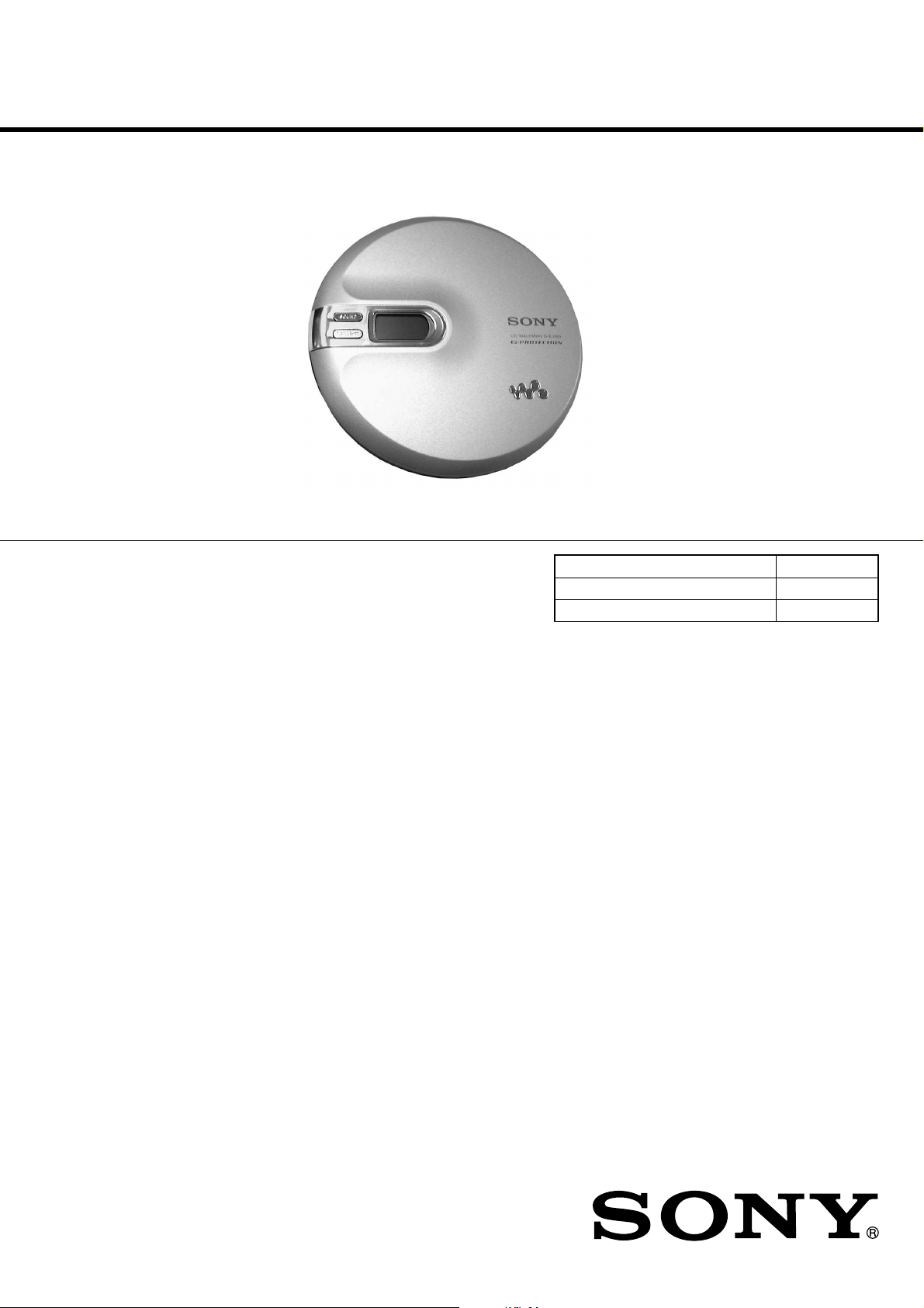
D-EJ760/EJ761/EJ765/EJ768CK
SERVICE MANUAL
Ver 1.0 2002.12
Photo : D-EJ760
AEP Model
D-EJ760/EJ761/EJ765
UK Model
D-EJ761
E Model
D-EJ761
Australian Model
D-EJ761/EJ768CK
Model Name Using Similar Mechanism NEW
CD Mechanism Type CDM-3325ER
Optical Pick-up Type DAX-25E
SPECIFICATIONS
System
Compact disc digital audio system
Laser diode properties
Material: GaAlAs
Wavelength: λ = 780 nm
Emission duration: Continuous
Laser output: Less than 44.6 µW (This output is the value measured at a distance of 200 mm from the objective lens surface on
the optical pick-up block with 7 mm aperture.)
Power requirements
For the area code of the model you purchased, check the upper
left side of the bar code on the package.
• Sony NH-WM2AA rechargeable batteries: 2.4 V DC
• Two LR6 (size AA) batteries: 3 V DC
• AC power adaptor (DC IN 4.5 V jack):
UK model: 230 V, 50 Hz
AUS model: 240 V, 50 Hz
AEP, E, EE models: 100 - 240 V, 50/60 Hz
Dimensions (w/h/d) (without projecting parts and controls)
Approx. 136.0 × 27.6 × 136.0 mm (5 3⁄8 × 1 1⁄8 × 5 3⁄8 in.)
Mass (excluding accessories)
Approx. 170 g (6.0 oz)
Operating temperature
5°C - 35°C (41°F - 95°F)
Design and specifications are subject to change without notice.
Supplied Accessories
D-EJ760: Headphones/earphones (1)
D-EJ761: AC power adaptor (1)
Headphones/earphones (1)
D-EJ765: AC power adaptor (1)
Headphones/earphones with remote control (1)
Rechargeable batteries (2)
Battery carrying case (1)
D-EJ768CK:
AC power adaptor (1)
Headphones/earphones (1)
Car connecting pack (1)
Car battery cord (1)
Rotary commander (1)
Velcro tape for the CD player (2)
Velcro tape for the rotary commander (1)
PORTABLE CD PLAYER
9-874-268-01
2002L0200-1
© 2002.12
Sony Corporation
Personal Audio Company
Pubulished by Sony Engineering Corporation

D-EJ760/EJ761/EJ765/EJ768CK
TABLE OF CONTENTS
• Abbreviation
AUS : Australian
EE : East European
DANGER
Invisible laser radiation when open and interlock failed or defeated.
Avoid direct exposure to beam.
CAUTION
Use of controls or adjustments or performance of procedures other
than those specified herein may result in hazardous radiation
exposure.
Flexible Circuit Board Repairing
• Keep the temperature of the soldering iron around 270°C during
repairing.
• Do not touch the soldering iron on the same conductor of the
circuit board (within 3 times).
• Be careful not to apply force on the conductor when soldering or
unsoldering.
Notes on chip component replacement
• Never reuse a disconnected chip component.
• Notice that the minus side of a tantalum capacitor may be damaged by heat.
Specifications ............................................................................ 1
1. SERVICING NOTES ................................................... 3
2. GENERAL
Locating the Controls ......................................................... 3
3. DISASSEMBLY
3-1. Cabinet (Upper) ASSY, Cabinet (Middle) ASSY ....... 4
3-2. MD ASSY, Main Board .............................................. 5
3-3. “Motor ASSY (Sled) (M902)”,
Optical Pick-up (DAX-25E),
“Motor ASSY, Turn Table (Spindle) (M901)” ............ 5
4. ELECTRICAL ADJUSTMENS ............................... 6
5. DIAGRAMS
5-1. Block Diagram ............................................................ 7
5-2. Schematic Diagram –MAIN SECTION (1/3)– ......... 8
5-3. Schematic Diagram –MAIN SECTION (2/3)– ......... 9
5-4. Schematic Diagram –MAIN SECTION (3/3)– ....... 10
5-5. Printed Wiring Boards ...............................................11
5-6. IC Pin Function Description ..................................... 13
6. EXPLODED VIEWS
6-1. Upper Lid Section ..................................................... 18
6-2. Cabinet Section ......................................................... 19
6-3. Optical pick-up Section (CDM-3325ER) ................. 20
7. ELECTRICAL PARTS LIST ................................... 21
SAFETY-RELATED COMPONENT WARNING!!
COMPONENTS IDENTIFIED BY MARK 0 OR DOTTED LINE
WITH MARK 0 ON THE SCHEMATIC DIAGRAMS AND IN THE
PA RTS LIST ARE CRITICAL TO SAFE OPERATION.
REPLACE THESE COMPONENTS WITH SONY PARTS WHOSE
PA RT NUMBERS APPEAR AS SHOWN IN THIS MANUAL OR IN
SUPPLEMENTS PUBLISHED BY SONY.
2
SECTION 1
SERVICING NOTES
NOTES ON HANDLING THE OPTICAL PICK-UP BLOCK OR
BASE UNIT
The laser diode in the optical pick-up block may suffer electrostatic
breakdown because of the potential difference generated by the charged
electrostatic load, etc. on clothing and the human body. During repair,
pay attention to electrostatic breakdown and also use the procedure in
the printed matter which is included in the repair parts.
The flexible board is easily damaged and should be handled with care.
NOTES ON LASER DIODE EMISSION CHECK
The laser beam on this model is concentrated so as to be focused on the
disc reflective surface by the objective lens in the optical pick-up block.
Therefore, when checking the laser diode emission, observe from more
than 30cm away from the objective lens.
Before Replacing the Optical pick-up Block
Please be sure to check thoroughly the parameters as per the “Optical
pick-up Block Checking Procedure” (Part No. : 9-960-027-11) issued
separately before replacing the optical Pick-up block.
Note and specifications required to check are given below.
• FOK output : IC601 yg pin
When checking FOK, remove the lead wire to disc motor.
• RF signal P-to-P value : 0.4 to 0.8Vp-p
D-EJ760/EJ761/EJ765/EJ768CK
Laser Diode Checking Methods
During normal operation of the equipment, emission of the laser diode
is prohibited unless the upper panel is closed while turning ON the S801
(push switch type).
The following two checking methods for the laser diode are operable.
Method :
Emission of the laser diode is visually checked.
1. Open the upper lid.
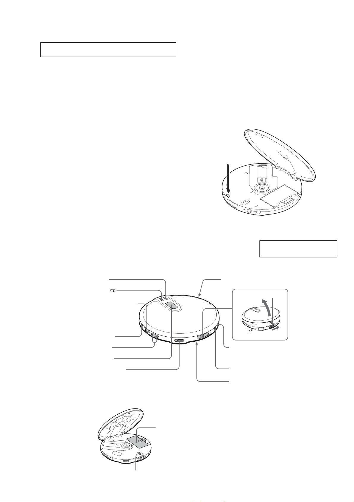
2. Push the S801 as shown in Fig. 1 .
3. Check the object lens for confirming normal emission of the laser
diode. If not emitting, there is a trouble in the automatic power
control circuit or the optical pick-up. During normal operation, the
laser diode is turned ON about 2.5 seconds for focus searching.
S801
LOCATING THE CONTROLS
CD player (front)
1 SOUND
2 P MODE/
34 Jog lever (u (play/
pause)•./> (AMS/
search))
5 CHARGE/x
6 VOL +*/–
Display
i (headphones) jack
*The button has a tactile dot.
SECTION 2
GENERAL
Fig.1 Method to push S801
This section is extracted from
instruction manual.
Strap holes
OPEN
DC IN 4.5 V (external power
input) jack
LINE OUT jack
7 HOLD
CD player (inside)
89 G-PROTECTION
BATTERY COMPARTMENT
3
D-EJ760/EJ761/EJ765/EJ768CK
Y
DISASSEMBLY
z
The equipment can be removed using the following procedure.
SECTION 3
MD ASSY “Motor ASSY, turn table (spindle) (M901)”, Optical pick-up (DAX-25E),
“Motor ASSY (Sled) (M902)”
Set
Cabinet (upper) ASSY,
Cabinet (middle) ASSY
Main board
Note : Follow the disassembly procedure in the numerical order given.
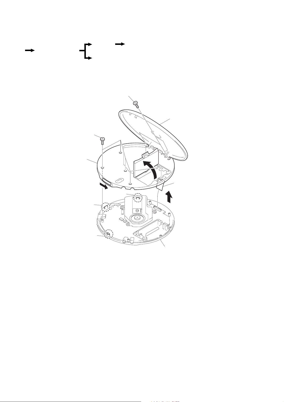
3-1. CABINET (UPPER) ASSY, CABINET (MIDDLE) ASSY
4 To w
screws (B2)
3 Five
screws (B2)
Cabinet (middle) ASSY
1
Cabinet (upper) ASS
2
7 CN801
5
Claw
5
Claw
5
Claw
6
Cabinet (lower) ASSY
4
3-2. MD ASSY, MAIN BOARD
Y
p
1 CN501
D-EJ760/EJ761/EJ765/EJ768CK
MD ASSY
2 CN502
3 CN503
4
Main board
5
Cabinet (lower) ASS
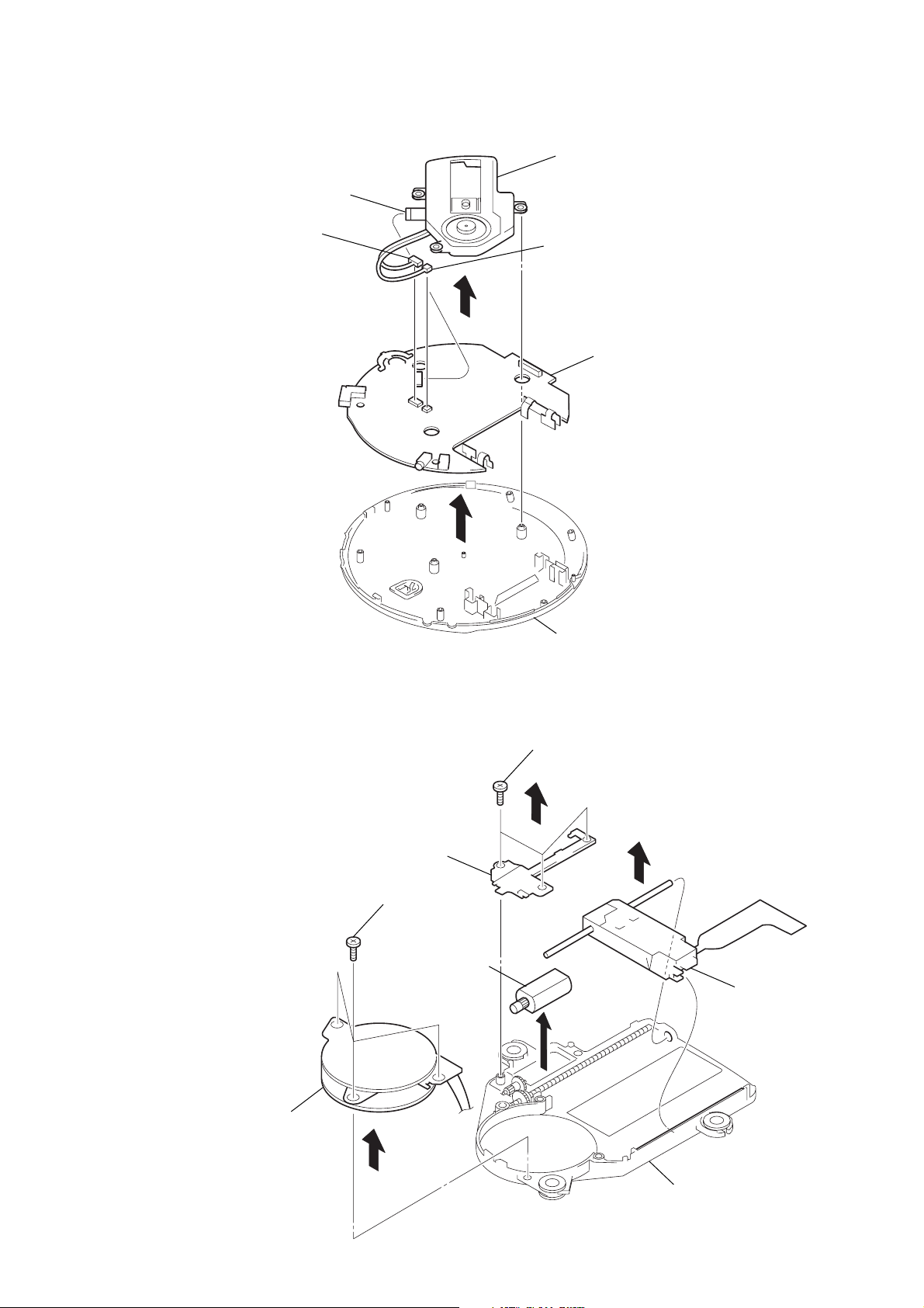
3-3. “MOTOR ASSY (SLED) (M902)”, OPTICAL PICK-UP (DAX-25E), “MOTOR ASSY, TURN TABLE (SPINDLE) (M901)”
1 Three screws
(B1.7x4)
2
Cover, Gear
5 Three screws
(B1.7x4)
Motor ASSY
(Sled) (M902)
3
Motor ASSY, Turn table
(Spindle) (M901)
4
Optical pick-u
(DAX-25E)
6
Chassis
5
D-EJ760/EJ761/EJ765/EJ768CK
)
D4
01
IC601
C627
C626
C611
C616
L606
R632
C602
C631
R627
C620
R601
C630
R624
R623
R622
C619
R621
C618
R620
C617
R625
C634
C633
C603
C632
C613
R635
C635
R636
C609
R619
C601
TP630
(RF)
60
61
90
91
SECTION 4
ELECTRICAL ADJUSTMENTS
The CD section adjustments are done automatically in this set.
Precautions for Check
1. Perform check in the order given.
2. Use YEDS-18 disc (Part No.: 3-702-101-01) unless otherwise
indicated.
3. Power supply voltage requirement : DC4.5 V in DC IN jack.
(J401)
VOLUME button : Minimum
HOLD switch : OFF
Focus bias Check
Condition:
• Hold the set in horizontal state.
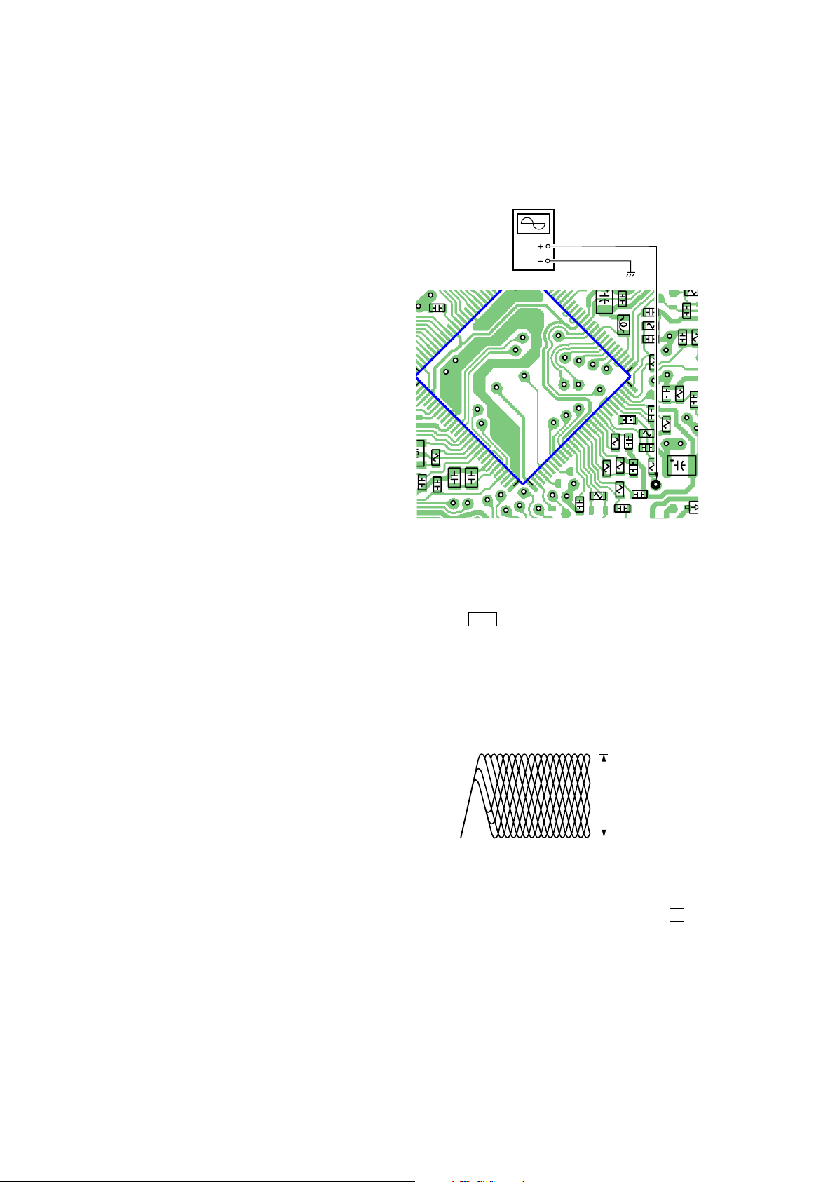
Connection:
oscilloscope
(AC range)
TP630(RF)
[MAIN BOARD] (SIDE A)
Procedure:
1. Connect the oscilloscope to the test point TP630(RF) on the
MAIN board.
2. Set a disc. (YEDS-18)
3. Press the u button.
4. Check the oscilloscope waveform is as shown below.
A good eye pattern means that the diamond shape (◊) in the center of the waveform can be clearly distinguished.
RF Signal reference Waveform (Eye Pattern)
VOLT/DIV : 100 mV (With the 10 : 1 probe in use
TIME/DIV : 500ns
RF level
0.4 to 0.8 Vp-p
To watch the eye pattern, set the oscilloscope to AC range and
increase the vertical sensitivity of the oscilloscope for easy
watch-ing.
5. Stop revolving of the disc motor by pressing the x button.
6
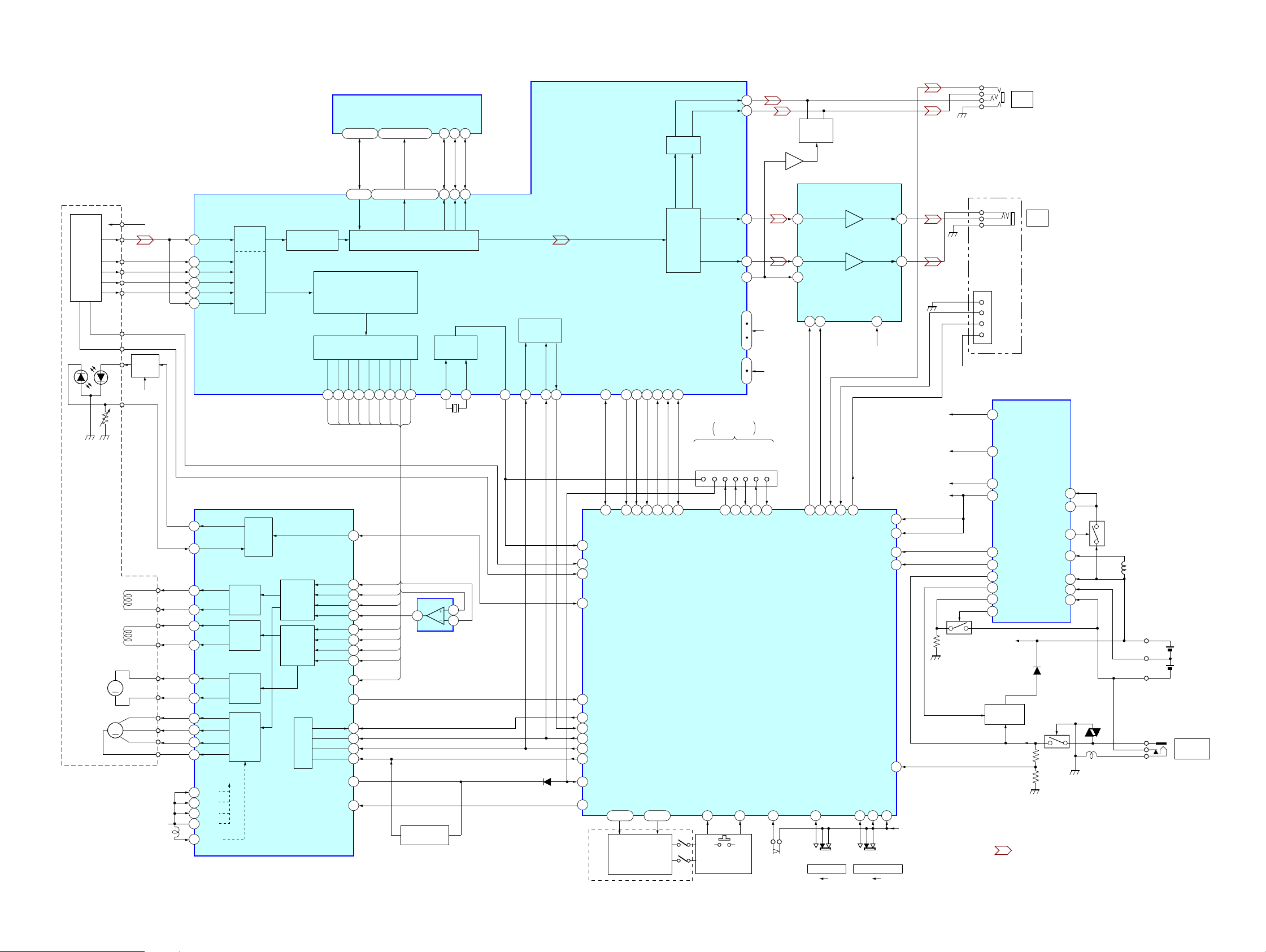
5-1. BLOCK DIAGRAM
OPTICAL
PICK-UP
BLOCK
(DAX-25E)
OP IC
FOCUS
COIL
TRACKING
COIL
M902
SLED
MOTOR
M901
SPINDLE
MOTOR
VCC
RF
OPGSW
OPSTB
LD
PD
M
M
A
A
E
F
VCC2_2.0V
LD
DRIVER
Q420
VCC1_2.2V
F+
F-
T+
T-
S+
S-
W
V
U
+VBAT
L430
84
92
91
89
90
88
22
23
48
46
44
42
52
50
80
53
49
45
41
6
4
2
1
RFAC
A
B
E
F
RFDC
SEO
SEM
FO2
RO2
FO3
RO3
FO1
RO1
W
U
V
COMCOM
VM1
VM12
VM23
VM3
SPVCC
RF
AMP
A/D
CH2
H
BRIDGE
CH3
H
BRIDGE
CH1
H
BRIDGE
CH4
H
BRIDGE
FOCUS/TRACKING COIL DRIVE
SLED/SPINDLE MOTOR DRIVE
DEMODULATOR
APC
LEVEL
SHIFTER
LEVEL
SHIFTER
IC401 (1/2)
SECTION 5
DIAGRAMS
IC603
D0-3 A0-9
1,2,24,25 5,9-12,14-18
4,3,6,5 113-116,11-13,15-17
D0-D3
EFM
SERVO
PWM
FFDR
FRDR
TFDR
TRDR
SFDR
SRDR
TRDR
SFDR
FFDR
FRDR
MDS
TFDR
TRDR
SFDR
SRDR
SYNC
SRDR
MDS
MDS
96 95 98 97 100 99 102 103 104 222120324748
FFDR
TFDR
FRDR
SEP
24
FI2
58
RI2
57
BRK
70
PWM
72 4
FI3
60
RI3
59
FI1
56
RI1
55
34
SYNC
74
FG
LATCH
40
DATA
CLOCK
WAKEUP
RSTOUT
XRST
39
38
37
35
36
I/F
RAM(4M)
A0-A9
SUB CODE
PROCESSOR
MDP
C176
MDP
SYNC
SYNC
MDP
COMPARATOR
DEFFERENTIAL
Q402
IC403
XRAS
XCAS
4 23 3
1 9 2
XCAS
XRAS
CLOCK
OSC
XTAO
X601
16.9MHz
3
1
XWE
XWE
XTAI
R4M
IC601
RF AMP,SERVO
DIGITAL SIGNAL PROCESSOR
D-RAM CONTROLLER
D/A CONVERTER
SIO
CLOCK_I
SDTO_I
SENS_O
78
77
70
72
75
16
17
18
66
D805
79
XIN
2
HG_GUP_O
HG_XSTB_O
AGCPWM_O
FG_I/FGSE_I
XPOWLT_O
MSDTI_I
MSDTO_O
MSCK_O
XWAKE_O
8
RESET
XRST_O
XRST_I
SCOR_O
WDCK_O
SYSM_I
SCOR_I
XRST_O
42-56 57-60
SEG0
I
SEG14
LIQUID
CRYSTAL
DISPLAY
SWITCH UNIT
AMUTE_O
GRSCOR_I
COM0
XSOE_I
XLAT_I
XLAT_O
XSOE_O
I
COM3
DAC
65232425262728
LPF
FOK
FOK_I
AOUT1
51
AOUT2
56
MUTE
DRIVE
Q302
HPL LOUT
43
HPR
LRMU
61
19
VDD0
|
72
105
50
57
P_SEL
P_SDTI
676873699151413121179
PGMSI_I
PGSEL_O
VCC3_2.65V
VCC2_2.0V
P_SDTO
TEST
PGMSO_O
VDD2
AVDD1
AVDD2
FLASH ROM
PROGRAM
RESET2
CLK4M2
CN901
P_SCK
PGMSCK_O
MUTE
Q301
LIN
8
RIN
9
MUTE
13
IC301
HEADPHONE AMP
PWRSW
BEEP
1114
3074 24
264
BEEP_O
AD_SEL
XPWRSW_O
IC801
SYSTEM
CONTROL
MICON
AD_KEY
AD_KEY2
2523 28 40
KEY MATRIX
S406 S404
S407 S405
CLOSE
S801
(OPEN/CLOSE)
HOLD_I
S803
.
HOLD
ON OFF
+V BAT
31
TSB_I/O
(EEPROM)
AD_RMKEY
AD_CHGMNT
AD_BATMNT
AD_DCINMNT
ESP_I
38
19
G.PROTECTION
ON OFF
6
ROUT
444
VCC
3
VCC3_2.65V
VCC2_2.0V
VCC1_2.2V
VCPU_2.0V
VDD1
5
VDD2
32
21
22 66
Q403
27
VCPU_AD
VREF_AD
20
VCPU_2.0V
S802
VCPU_2.0V
D-EJ760/EJ761/EJ765/EJ768CK
J301
LINE
OUT
J302
i
IC401 (2/2)
POWER CONTROL
11
VCC3
VCC2
18
17
VCC1
19
VCPU
CHGMNT_O
67
VMMNT_O
DCIN
61
REGB
62
DET(0.29V)
63
CHGB
65
+VBAT
SWITCH
Q401, 405
• SIGNAL PATH
BATM1_I
BATM2_I
D400
: CD PLAY
VCC0_I
VCC0_O
STNG
VIN
Q412
20
16
Q404
25
VDR409
L401
DRY BATTERY
SIZE "AA"
(IEC DESIGNATION LR6)
2PCS, 3V
RECHARGEABLE BATTERY
OR
NC-WMAA/NH-WM2AA
2.4V
J401
DC IN 4.5V
LG
8
12
68
69
!
77
D-EJ760/EJ761/EJ765/EJ768CK
5-2. SCHEMATIC DIAGRAM – MAIN SECTION (1/3) – • Refer to page 12 for Notes. • Refer to page 13 for IC Pin Function Description.
M902
TRACKING
COIL
TP630
RF
E
F
B
A
C502
4.7
M901
R637
22k
R639
22k
R632
R631
22k
Q301
XP4501
<M>
C202
1000p
C110
2.2
C357
22
6.3V
IC603
4M DRAM
MUTE
C102
1000p
C358
2200p
R353
C354
100
6.3V
R205
R105
1k
1k
L201
4.7µH
L101
L301
4.7µH
D302
MM3Z5VT1
D305
C816
MM3Z5VT1
100p
Q302
XP4312
<M>
MUTE
DRIVE
R360
0
C360
1000p
R111
C111
470
220
4V
C211
220
4V
R211
470
C361
1000p
R361
0
4.7
L303
0
4.7µH
EJ761:AUS,E/EJ768CK
R823
*R823
47k
EJ760/EJ761:AEP,EE,UK/EJ765
100k
EJ761:AUS,E/EJ768CK
L310
4.7µH
L110
4.7µH
L210
4.7µH
CN502
4P
1
4
1
2
CN501
15P
15
10
FOCUS
COIL
C617
4700p
C618
0.47
R621
C601
C602
47
0.1
4V
(RF)
C631
47k
22p
R633
R635
22k
22k
AVDD
5
1
C616
1M
C619
R634
100k
C634
470p
R1
0
CN503
WHITE
<SLED>
0.1
R620
0.47
R624
C620
R627
W
V
U
2P
0
OPGSW
OPSTB
R618
10k
R622
C632
470p
S+
LD
PD
T+
470k
100p
C630
2200p
COM
C606
0.1
L603
C101
R613
2.2k
C625
6.3V
C201
4.7
10
R609
R608
R607
R606
C609
4.7
C605
0.47
XCAS
XWE
XRAS
A4
A5
A6
A7
A8
A9
D2
D3
D0
D1
W
V
U
C612
R615
22
22
6.3V
0
S-
A
B
RF
E
F
F+
T-
F-
2.2k
220k
R623
R601
C633
470p
C635
470p
FOK
2.2k
R619
10k
R636
100k
C615
0.1
47k
L606
10µH
DVDD
R2
0
C603
0.1
C611
C627
FRDR
C613
0.1
0.1
C626
2.2
2.2
R
R
DR
TFD
TR
FFD
L601
0
L605
X601
16.9MHz
R625
0
IC601
CXD3039AR
DSP IC
SYNC
C604
10
4V
10p
C622
R603
C610
C608
47
1
4V
L604
R614
220
R626
0
0
L320
A3
A2
A1
0
C607
47p
A0
10p
C621
DR
SFDR
SR
DS
DP
M
M
L602
0
470
470
470
470
100p
R612
100k
GRSCOR
AMUTE
MSDTI
MSDTO
R4M
XRST
SCOR
XSOE
XLAT
MSCK
R206
100k
BEEP
XPWRSW
R106
100k
C351
0.22
C352
22
6.3V
C355
1000p
C628
2.2
A3
R225
10k
R223
4.7k
R224
2.2k
C210
2.2
A2
R201
220
R101
220
C222
470p
C223
470p
C224
470p
C353
22
6.3V
A0
A1
C122
470p
C123
470p
C124
470p
*R112,212
4.7k
EJ760/EJ761:AEP,EE,UK/EJ765
100k
EJ761:AUS,E/EJ768CK
R212
*
R210
22k
A9
AS
XR
R112
*
R110
22k
IC301
AN17881F-E1
0
1
E
D
D
W
X
R125
10k
R123
4.7k
R124
2.2k
IC41SV4105-100TG
*
R824
470k
303
VDR
C312
1000p
R316
R315
4.7µH
VDR101
R102
VD
1k
10k
L302
VDR201
202
VDR
D306
MM3Z5VT1
R317
0
D304
MM3Z5VT1
D303
MM3Z5VT1
D301
MM3Z5VT1
J302
J301
LINE
OUT
BUS-3
VCC3_2.65V
VCC
S-2
BU
VCC2_2.0V
6
A4
A
A5
A8
A7
-2
G
VIN
8
BUS-1
8
AS
D2
XC
D3
-1
G
2.0V
PU_
VC
SEL
AD
B_I/O
TS
KEY
M
R
AD
Loading...