


NSC LM2612BTLX, LM2612BTL, LM2612BBLX, LM2612BBL, LM2612ATLX Datasheet
...December 2002
LM2612BL
400mA Sub-miniature, Programmable, Step-Down DC-DC Converter for Ultra Low-Voltage Circuits
General Description
The LM2612 step-down DC-DC converter is optimized for powering ultra-low voltage circuits from a single Lithium-Ion cell. It provides up to 400mA (300mA for B grade), over an input voltage range of 2.8V to 5.5V. Pin programmable output voltages of 1.05V, 1.3V, 1.5V or 1.8V allow adjustment for MPU voltage options without board redesign or external feedback resistors.
The device has three pin-selectable modes for maximizing battery life in mobile phones and similar portable applications. Low-noise PWM mode offers 600kHz fixed-frequency operation to reduce interference in RF and data acquisition applications during full-power operation. In PWM mode, internal synchronous rectification provides high efficiency (91% typ. at 1.8VOUT). A SYNC input allows synchronizing the switching frequency in a range of 500kHz to 1MHz to avoid noise from intermodulation with system frequencies. Low-current hysteretic PFM mode reduces quiescent current to 160 µA (typ.) during system standby. Shutdown mode turns the device off and reduces battery consumption to 0.02µA (typ.). Additional features include soft start and current overload protection.
The LM2612 is available in a 10 pin micro SMD packge. This package uses National’s wafer level chip-scale micro SMD technology and offers the smallest possible size. Only three small external surface-mount components, an inductor and two ceramic capacitors are required.
Key Specifications
nOperates from a single LiION cell (2.8V to 5.5V)
nInternal synchronous rectification for high PWM mode efficiency
nPin programmable output voltage (1.05V, 1.3V, 1.5V and 1.8V)
n400mA maximum load capability (300mA for B grade)
n±2% PWM mode DC output voltage precision
n5mV typ PWM mode output voltage ripple
n160 µA typ PFM mode quiescent current
n0.02µA typ shutdown mode current
n600kHz PWM mode switching frequency
nSYNC input for PWM mode frequency synchronization from 500kHz to 1MHz
Features
nSub-miniature 10-pin micro SMD package
nOnly three tiny surface-mount external components required
nUses small ceramic capacitors
nInternal soft start
nCurrent overload protection
nNo external compensation required
nThermal shutdown protection
Applications
nMobile Phones
nHand-Held Radios
nBattery Powered Devices
Typical Application Circuit
20041802
Ultra for Converter DC-DC Down-Step Programmable, miniature,-Sub 400mA LM2612BL
Circuits Voltage-Low
© 2002 National Semiconductor Corporation |
DS200418 |
www.national.com |
LM2612BL
Connection Diagrams
micro SMD package
20041804 |
20041805 |
TOP VIEW |
BOTTOM VIEW |
Ordering Information
Order Number |
|
Package Type |
NSC Package |
Supplied As |
|
|
|
Marking(*) |
|
|
|
|
|
|
10-Pin micro SMD |
|
|
|
|
|
|
|
|
|
LM2612ABL |
|
BLP106WB |
XYTT IS41A |
250 Units, Tape and Reel |
|
|
|
|
|
LM2612BBL |
|
XYTT IS41B |
250 Units, Tape and Reel |
|
|
10-bump Wafer Level Chip Scale |
|||
|
|
|
|
|
LM2612ABLX |
|
XYTT IS41A |
3000 Units, Tape and Reel |
|
|
(micro SMD) |
|||
|
|
|
|
|
LM2612BBLX |
|
XYTT IS41B |
3000 Units, Tape and Reel |
|
|
|
|||
|
|
|
|
|
(*) XY - denotes the date code marking (2 digit) in production |
|
|
||
TT - refers to die run/lot traceability for production |
|
|
||
I - pin one indication |
|
|
|
|
S - Product line designator |
|
|
|
|
Note the Package Marking may change over the course of production time without notice |
|
|||
Order Number |
|
Package Type |
NSC Package |
Supplied As |
|
|
|
Marking(*) |
|
|
|
|
|
|
10-Pin micro SMD |
|
|
|
|
|
|
|
|
|
LM2612ATL |
|
TLP106WA |
XYTT IS41A |
250 Units, Tape and Reel |
|
|
|
|
|
LM2612BTL |
|
XYTT IS41B |
250 Units, Tape and Reel |
|
|
10-bump Wafer Level Chip Scale |
|||
|
|
|
|
|
LM2612ATLX |
|
XYTT IS41A |
3000 Units, Tape and Reel |
|
|
(micro SMD) |
|||
|
|
|
|
|
LM2612BTLX |
|
XYTT IS41B |
3000 Units, Tape and Reel |
|
|
|
|||
|
|
|
|
|
(*) XY - denotes the date code marking (2 digit) in production |
|
|
||
TT - refers to die run/lot traceability for production |
|
|
||
I - pin one indication |
|
|
|
|
S - Product line designator |
|
|
|
|
Note the Package Marking may change over the course of production time without notice
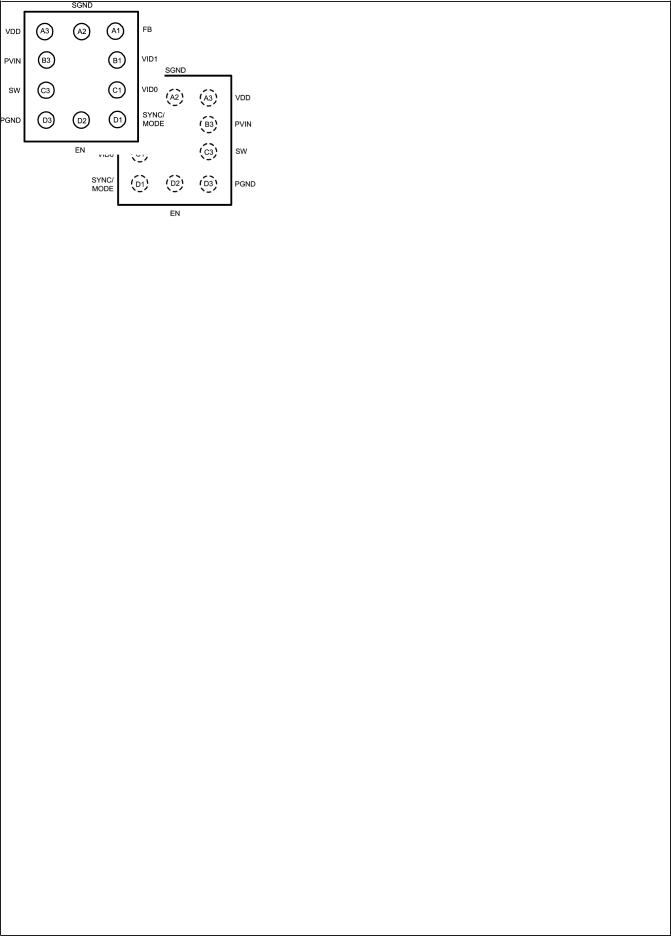
Pin Description
Pin Number |
Pin Name |
Function |
|
|
|
A1 |
FB |
Feedback Analog Input. Connect to the output at the output filter capacitor (Figure 1) |
|
|
|
B1 |
VID1 |
Output Voltage Control Inputs. Set the output voltage using these digital inputs (see Table |
|
|
1). The output defaults to 1.5V if these pins are unconnected. |
C1 |
VID0 |
|
|
|
|
D1 |
SYNC/MODE |
Synchronization Input. Use this digital input for frequency synchronization or modulation |
|
|
control. Set: |
|
|
SYNC/MODE = high for low-noise 600kHz PWM mode |
|
|
SYNC/MODE = low for low-current PFM mode |
|
|
SYNC/MODE = 500kHz - 1MHz external clock for synchronization to an external clock in |
|
|
PWM mode. See Synchronization and Operating Modes in the Device Information section. |
|
|
|
D2 |
EN |
Enable Input. For shutdown, set low to SGND.(See Shutdown Mode in the Device |
|
|
Information section.) |
|
|
|
D3 |
PGND |
Power Ground |
|
|
|
www.national.com |
2 |

Pin Description (Continued)
Pin Number |
Pin Name |
Function |
|
|
|
C3 |
SW |
Switching Node connection to the internal PFET switch and NFET synchronous rectifier. |
|
|
|
B3 |
PVIN |
Power Supply Input to the internal PFET switch. Connect to the input filter capacitor |
|
|
(Figure 1). |
|
|
|
A3 |
VDD |
Analog Supply Input. If board layout is not optimum, an optional 0.1µF ceramic capacitor |
|
|
is suggested (Figure 1) |
|
|
|
A2 |
SGND |
Analog and Control Ground |
|
|
|
(*) Note that the pin numbering scheme for the Micro SMD package was revised in April, 2002 to conform to JEDEC standard. Only the pin numbers were revised. No changes to the physical location of the inputs/outputs were made. For reference purpose, the obselete numbering had FB as pin 1, VID1 as pin 2, VID0 as pin 3, SYNC as pin 4, EN as pin 5, PGND as pin 6, SW as pin 7, PVIN as pin 8, VDD as pin 9 and SGND as pin 10.
LM2612BL
3 |
www.national.com |

LM2612BL
Absolute Maximum Ratings (Note 1)
If Military/Aerospace specified devices are required, please contact the National Semiconductor Sales Office/ Distributors for availability and specifications.
PVIN, VDD, to SGND |
−0.2V to +6V |
PGND to SGND |
−0.2V to +0.2V |
EN, SYNC/MODE, VID0, VID1 to |
|
SGND |
−0.2V to +6V |
FB, SW |
(GND −0.2V) to |
|
(VDD +0.2V) |
Storage Temperature Range |
−45˚C to +150˚C |
Lead temperature |
|
(Soldering, 10 sec.) |
260˚C |
Junction Temperature (Note 2) |
−25˚C to 125˚C |
Minimum ESD Rating |
|
Human body model, C = 100pF, R = |
|
1.5 kΩ |
±2kV |
Thermal Resistance (θJA) |
|
LM2612ABL/LM2612ATL & |
|
LM2612BBL/LM2612BTL(Note 3) |
140˚C/W |
Electrical Characteristics
Specifications with standard typeface are for TA = TJ = 25˚C, and those in bold face type apply over the full Operating Temperature Range (TA = TJ = −25˚C to +85˚C). Unless otherwise specified, PVIN = VDD = EN = SYNC = 3.6V, VID0 = VID1 = 0V.
Symbol |
Parameter |
Conditions |
Min |
Typ |
Max |
Units |
|
|
|
|
|
|
|
|
|
VIN |
Input Voltage Range (Note |
PVIN = VDD = VID1 = VIN, |
2.8 |
|
5.5 |
V |
|
|
4) |
VID0 = 0V |
|
||||
|
|
|
|
|
|||
|
|
|
|
|
|
|
|
|
|
VID0 = VIN, VID1 = VIN |
1.029 |
1.05 |
1.071 |
|
|
VFB |
Feedback Voltage |
VID0 = VIN, VID1 = 0V |
1.274 |
1.30 |
1.326 |
V |
|
(Note 5) |
VID0 = 0V, VID1 = 0V |
1.470 |
1.50 |
1.530 |
|||
|
|
||||||
|
|
|
|
|
|
|
|
|
|
VID0 = 0V, VID1 = VIN |
1.764 |
1.8 |
1.836 |
|
|
VHYST |
PFM Comparator Hysteresis |
PFM Mode (SYNC = 0V) |
|
|
|
|
|
|
Voltage |
|
|
25 |
|
mV |
|
|
(Note 6) |
|
|
|
|
|
|
|
|
|
|
|
|
|
|
ISHDN |
Shutdown Supply Current |
EN = 0V |
|
0.02 |
3 |
µA |
|
IQ1 |
DC Bias Current into VDD |
No switching, PFM mode |
|
160 |
195 |
|
|
|
|
(SYNC/MODE = 0V) |
|
|
|||
|
|
|
|
|
µA |
||
|
|
|
|
|
|
||
IQ2 |
|
No switching, PWM mode |
|
605 |
725 |
||
|
|
|
|||||
|
|
(SYNC/MODE = VIN) |
|
|
|||
|
|
|
|
|
|
||
RDSON (P) |
Pin-Pin Resistance for P |
|
|
395 |
550 |
mΩ |
|
|
FET |
|
|
||||
|
|
|
|
|
|
||
|
|
|
|
|
|
|
|
RDSON (N) |
Pin-Pin Resistance for N |
|
|
325 |
500 |
mΩ |
|
|
FET |
|
|
||||
|
|
|
|
|
|
||
|
|
|
|
|
|
|
|
RDSON , TC |
FET Resistance |
|
|
0.5 |
|
%/C |
|
|
Temperature Coefficient |
|
|
|
|||
|
|
|
|
|
|
||
|
|
|
|
|
|
|
|
Ilim |
Switch Peak Current Limit |
LM2612ABL/LM2612ATL |
510 |
710 |
850 |
mA |
|
|
(Note 7) |
LM2612BBL/LM2612BTL |
400 |
710 |
980 |
||
|
|
||||||
|
|
|
|
|
|
|
|
VEN_H |
EN Positive Going |
|
|
0.95 |
1.3 |
V |
|
|
Threshold Voltage |
|
|
||||
|
|
|
|
|
|
||
|
|
|
|
|
|
|
|
VEN_L |
EN Negative Going |
|
0.4 |
0.80 |
|
V |
|
|
Threshold Voltage |
|
|
||||
|
|
|
|
|
|
||
|
|
|
|
|
|
|
|
VSYNC_H |
SYNC/MODE Positive |
|
|
0.95 |
1.3 |
V |
|
|
Going Threshold Voltage |
|
|
||||
|
|
|
|
|
|
||
|
|
|
|
|
|
|
|
VSYNC_L |
SYNC/MODE Negative |
|
0.4 |
0.84 |
|
V |
|
|
Going Threshold Voltage |
|
|
||||
|
|
|
|
|
|
||
|
|
|
|
|
|
|
|
VID_H |
VID0, VID1 Positive Going |
|
|
0.92 |
1.3 |
V |
|
|
Threshold Voltage |
|
|
||||
|
|
|
|
|
|
||
|
|
|
|
|
|
|
|
VID_L |
VID0, VID1 Negative Going |
|
0.4 |
0.83 |
|
V |
|
|
Threshold Voltage |
|
|
||||
|
|
|
|
|
|
||
|
|
|
|
|
|
|
|
IVID |
VID1, VID0 Pull Down |
VID1, VID0 = 3.6V |
|
1.8 |
3.0 |
µA |
|
|
Current |
|
|
||||
|
|
|
|
|
|
||
|
|
|
|
|
|
|
www.national.com |
4 |

Electrical Characteristics (Continued)
Specifications with standard typeface are for TA = TJ = 25˚C, and those in bold face type apply over the full Operating Temperature Range (TA = TJ = −25˚C to +85˚C). Unless otherwise specified, PVIN = VDD = EN = SYNC = 3.6V, VID0 = VID1 = 0V.
Symbol |
Parameter |
Conditions |
Min |
Typ |
Max |
Units |
|
|
|
|
|
|
|
fsync |
SYNC/MODE Clock |
|
|
|
|
|
|
Frequency Range |
|
500 |
|
1000 |
kHz |
|
(Note 8) |
|
|
|
|
|
|
|
|
|
|
|
|
FOSC |
Internal Oscillator |
LM2612ABL/ATL, PWM Mode |
468 |
600 |
732 |
|
|
Frequency |
(SYNC = VIN) |
|
|||
|
|
|
|
kHz |
||
|
|
|
|
|
|
|
|
|
LM2612BBL/BTL, PWM Mode |
450 |
600 |
750 |
|
|
|
|
||||
|
|
(SYNC = VIN) |
|
|||
|
|
|
|
|
|
|
|
|
|
|
|
|
|
Tmin |
Minimum ON-Time of P FET |
|
|
200 |
|
nS |
|
Switch in PWM Mode |
|
|
|
||
|
|
|
|
|
|
|
|
|
|
|
|
|
|
Note 1: Absolute Maximum Ratings indicate limits beyond which damage to the device may occur. Operating Ratings are conditions for which the device is intended to be functional, but parameter specifications may not be guaranteed. For guaranteed specifications and associated test conditions, see the Min and Max limits and Conditions in the Electrical Characteristics table. Electrical Characteristics table limits are guaranteed by production testing, design or correlation using standard Statistical Quality Control methods. Typical (Typ) specifications are mean or average values from characterization at 25˚C and are not guaranteed.
Note 2: Thermal shutdown will occur if the junction temperature exceeds the 150˚C maximum junction temperature of the device.
Note 3: Thermal resistance specified with 2 layer PCB(0.5/0.5 oz. cu).
Note 4: The LM2612 is designed for applications where turn-on after system power-up is controlled by the system processor and internal UVLO (Under Voltage LockOut) circuitry is unnecessary. The LM2612 has no UVLO circuitry and should be kept in shutdown by holding the EN pin low until the input voltage exceeds 2.8V. Although the LM2612 exhibits safe behavior while enabled at low input voltages, this is not guaranteed.
Note 5: The feedback voltage is trimmed at the 1.5V output setting. The other output voltages result from the pin selection of the internal DAC’s divider ratios. The precision for the feedback voltages is ±2%.
Note 6: : The hysteresis voltage is the minimum voltage swing on FB that causes the internal feedback and control circuitry to turn the internal PFET switch on and then off during PFM mode.
Note 7: Current limit is built-in, fixed, and not adjustable. If the current limit is reached while the output is pulled below about 0.7V, the internal PFET switch turns off for 2.5 µs to allow the inductor current to diminish.
Note 8: SYNC driven with an external clock switching between VIN and GND. When an external clock is present at SYNC, the IC is forced to PWM mode at the external clock frequency. The LM2612 synchronizes to the rising edge of the external clock.
LM2612BL
5 |
www.national.com |

LM2612BL
Typical Operating Characteristics LM2612ABL/ATL, Circuit of Figure 1, VIN = 3.6V, TA = 25˚C, L1 = 10 µH, unless otherwise noted.
Quiescent Supply Current vs Temperature |
Quiescent Supply Current vs Supply Voltage |
20041806
Shutdown Quiescent Current vs Temperature
20041808
Output Voltage vs Temperature (PFM Mode)
20041807
Output Voltage vs Temperature (PWM Mode)
20041809
Output Voltage vs Supply Voltage (VOUT = 1.5V, PWM Mode)
20041810 |
20041813 |
www.national.com |
6 |
 Loading...