


NSC LM2588T-ADJ, LM2588T-5.0, LM2588T-12, LM2588SX-ADJ, LM2588SX-5.0 Datasheet
...
April 1998
LM2588
SIMPLE SWITCHER® 5A Flyback Regulator with Shutdown
General Description
The LM2588 series of regulators are monolithic integrated circuits specifically designed for flyback, step-up (boost), and forward converter applications. The device is available in 4 different output voltage versions: 3.3V, 5.0V, 12V, and adjustable.
Requiring a minimum number of external components, these regulators are cost effective, and simple to use. Included in the datasheet are typical circuits of boost and flyback regulators. Also listed are selector guides for diodes and capacitors and a family of standard inductors and flyback transformers designed to work with these switching regulators.
The power switch is a 5.0A NPN device that can stand-off 65V. Protecting the power switch are current and thermal limiting circuits, and an undervoltage lockout circuit. This IC contains an adjustable frequency oscillator that can be programmed up to 200 kHz. The oscillator can also be synchronized with other devices, so that multiple devices can operate at the same switching frequency.
Other features include soft start mode to reduce in-rush current during start up, and current mode control for improved rejection of input voltage and output load transients and cycle-by-cycle current limiting. The device also has a shutdown pin, so that it can be turned off externally. An output voltage tolerance of ±4%, within specified input voltages and output load conditions, is guaranteed for the power supply system.
Features
nRequires few external components
nFamily of standard inductors and transformers
nNPN output switches 5.0A, can stand off 65V
nWide input voltage range: 4V to 40V
nAdjustable switching frequency: 100 kHz to 200 kHz
nExternal shutdown capability
nDraws less than 60 µA when shut down
nFrequency synchronization
nCurrent-mode operation for improved transient response, line regulation, and current limit
nInternal soft-start function reduces in-rush current during start-up
nOutput transistor protected by current limit, under voltage lockout, and thermal shutdown
nSystem output voltage tolerance of ±4% max over line and load conditions
Typical Applications
nFlyback regulator
nForward converter
nMultiple-output regulator
nSimple boost regulator
Flyback Regulator
DS012420-1
SIMPLE SWITCHER® and Switchers Made Simple ® are registered trademarks of National Semiconductor Corporation.
Shutdown with Regulator Flyback 5A SWITCHER SIMPLE LM2588
© 1999 National Semiconductor Corporation |
DS012420 |
www.national.com |

Ordering Information
Package Type |
NSC Package |
Order Number |
|
|
|
Drawing |
|
|
|
|
|
7-Lead TO-220 |
Bent, Staggered Leads |
TA07B |
LM2588T-3.3, LM2588T-5.0, LM2588T-12, LM2588T-ADJ |
|
|
|
|
7-Lead TO-263 |
|
TS7B |
LM2588S-3.3, LM2588S-5.0, LM2588S-12, LM2588S-ADJ |
|
|
|
|
7-Lead TO-263 |
Tape and Reel |
TS7B |
LM2588SX-3.3, LM2588SX-5.0, LM2588SX-12, |
|
|
|
LM2588SX-ADJ |
|
|
|
|
www.national.com |
2 |

Absolute Maximum Ratings (Note 1)
If Military/Aerospace specified devices are required, please contact the National Semiconductor Sales Office/ Distributors for availability and specifications.
Input Voltage |
−0.4V |
≤ VIN ≤ 45V |
||
Switch Voltage |
−0.4V |
≤ VSW ≤ 65V |
||
Switch Current (Note 2) |
Internally Limited |
|||
Compensation Pin Voltage |
−0.4V |
≤ VCOMP ≤ 2.4V |
||
Feedback Pin Voltage |
−0.4V |
≤ VFB ≤ 2 VOUT |
||
ON |
/OFF Pin Voltage |
−0.4V ≤ VSH ≤ 6V |
||
Sync Pin Voltage |
−0.4V ≤ VSYNC ≤ 2V |
|||
Power Dissipation (Note 3) |
Internally Limited |
|||
Storage Temperature Range |
|
−65ÊC to +150ÊC |
||
Lead Temperature |
|
(Soldering, 10 sec.) |
260ÊC |
Maximum Junction Temperature |
|
(Note 3) |
150ÊC |
Minimum ESD Rating |
|
(C = 100 pF, R = 1.5 kΩ) |
2 kV |
Operating Ratings
Supply Voltage |
4V ≤ VIN ≤ 40V |
Output Switch Voltage |
0V ≤ VSW ≤ 60V |
Output Switch Current |
ISW ≤ 5.0A |
Junction Temperature Range |
−40ÊC ≤ TJ ≤ +125ÊC |
LM2588-3.3
Electrical Characteristics
Specifications with standard type face are for TJ = 25ÊC, and those in bold type face apply over full Operating Temperature Range. Unless otherwise specified, VIN = 5V.
Symbol |
Parameters |
Conditions |
Typical |
Min |
Max |
Units |
|
|
|
|
|
|
|
SYSTEM PARAMETERS Test Circuit of Figure 1 (Note 4) |
|
|
|
|
||
|
|
|
|
|
|
|
VOUT |
Output Voltage |
VIN = 4V to 12V |
3.3 |
3.17/3.14 |
3.43/3.46 |
V |
|
|
ILOAD = 400 mA to 1.75A |
|
|
|
|
VOUT/ |
Line Regulation |
VIN = 4V to 12V |
20 |
|
50/100 |
mV |
VIN |
|
ILOAD = 400 mA |
|
|
|
|
VOUT/ |
Load Regulation |
VIN = 12V |
20 |
|
50/100 |
mV |
ILOAD |
|
ILOAD = 400 mA to 1.75A |
|
|
|
|
η |
Efficiency |
VIN = 12V, ILOAD = 1A |
75 |
|
|
% |
UNIQUE DEVICE PARAMETERS (Note 5) |
|
|
|
|
||
|
|
|
|
|
|
|
VREF |
Output Reference |
Measured at Feedback Pin |
3.3 |
3.242/3.234 |
3.358/3.366 |
V |
|
Voltage |
VCOMP = 1.0V |
|
|
|
|
VREF |
Reference Voltage |
VIN = 4V to 40V |
2.0 |
|
|
mV |
|
Line Regulation |
|
|
|
|
|
|
|
|
|
|
|
|
GM |
Error Amp |
ICOMP = −30 µA to +30 µA |
1.193 |
0.678 |
2.259 |
mmho |
|
Transconductance |
VCOMP = 1.0V |
|
|
|
|
AVOL |
Error Amp |
VCOMP = 0.5V to 1.6V |
260 |
151/75 |
|
V/V |
|
Voltage Gain |
RCOMP = 1.0 MΩ (Note 6) |
|
|
|
|
LM2588-5.0
Electrical Characteristics
Specifications with standard type face are for TJ = 25ÊC, and those in bold type face apply over full Operating Temperature Range. Unless otherwise specified, VIN = 5V.
Symbol |
Parameters |
Conditions |
Typical |
Min |
Max |
Units |
|
|
|
|
|
|
|
SYSTEM PARAMETERS Test Circuit of Figure 1 (Note 4) |
|
|
|
|
||
|
|
|
|
|
|
|
VOUT |
Output Voltage |
VIN = 4V to 12V |
5.0 |
4.80/4.75 |
5.20/5.25 |
V |
|
|
ILOAD = 500 mA to 1.45A |
|
|
|
|
VOUT/ |
Line Regulation |
VIN = 4V to 12V |
20 |
|
50/100 |
mV |
VIN |
|
ILOAD = 500 mA |
|
|
|
|
VOUT/ |
Load Regulation |
VIN = 12V |
20 |
|
50/100 |
mV |
ILOAD |
|
ILOAD = 500 mA to 1.45A |
|
|
|
|
η |
Efficiency |
VIN = 12V, ILOAD = 750 mA |
80 |
|
|
% |
UNIQUE DEVICE PARAMETERS (Note 5) |
|
|
|
|
||
|
|
|
|
|
|
|
VREF |
Output Reference |
Measured at Feedback Pin |
5.0 |
4.913/4.900 |
5.088/5.100 |
V |
|
Voltage |
VCOMP = 1.0V |
|
|
|
|
3 |
www.national.com |

LM2588-5.0
Electrical Characteristics (Continued)
Specifications with standard type face are for TJ = 25ÊC, and those in bold type face apply over full Operating Temperature Range. Unless otherwise specified, VIN = 5V.
Symbol |
Parameters |
Conditions |
Typical |
Min |
Max |
Units |
|
|
|
|
|
|
|
UNIQUE DEVICE PARAMETERS (Note 5) |
|
|
|
|
||
|
|
|
|
|
|
|
VREF |
Reference Voltage |
VIN = 4V to 40V |
3.3 |
|
|
mV |
|
Line Regulation |
|
|
|
|
|
|
|
|
|
|
|
|
GM |
Error Amp |
ICOMP = −30 µA to +30 µA |
0.750 |
0.447 |
1.491 |
mmho |
|
Transconductance |
VCOMP = 1.0V |
|
|
|
|
AVOL |
Error Amp |
VCOMP = 0.5V to 1.6V |
165 |
99/49 |
|
V/V |
|
Voltage Gain |
RCOMP = 1.0 MΩ (Note 6) |
|
|
|
|
LM2588-12
Electrical Characteristics
Specifications with standard type face are for TJ = 25ÊC, and those in bold type face apply over full Operating Temperature Range. Unless otherwise specified, VIN = 5V.
Symbol |
Parameters |
Conditions |
Typical |
Min |
Max |
Units |
SYSTEM PARAMETERS Test Circuit of Figure 2 (Note 4) |
|
|
|
|
||
|
|
|
|
|
|
|
VOUT |
Output Voltage |
VIN = 4V to 10V |
12.0 |
11.52/11.40 |
12.48/12.60 |
V |
|
|
ILOAD = 300 mA to 1.2A |
|
|
|
|
VOUT/ |
Line Regulation |
VIN = 4V to 10V |
20 |
|
100/200 |
mV |
VIN |
|
ILOAD = 300 mA |
|
|
|
|
VOUT/ |
Load Regulation |
VIN = 10V |
20 |
|
100/200 |
mV |
ILOAD |
|
ILOAD = 300 mA to 1.2A |
|
|
|
|
η |
Efficiency |
VIN = 10V, ILOAD = 1A |
90 |
|
|
% |
UNIQUE DEVICE PARAMETERS (Note 5) |
|
|
|
|
||
|
|
|
|
|
|
|
VREF |
Output Reference |
Measured at Feedback Pin |
12.0 |
11.79/11.76 |
12.21/12.24 |
V |
|
Voltage |
VCOMP = 1.0V |
|
|
|
|
VREF |
Reference Voltage |
VIN = 4V to 40V |
7.8 |
|
|
mV |
|
Line Regulation |
|
|
|
|
|
|
|
|
|
|
|
|
GM |
Error Amp |
ICOMP = −30 µA to +30 µA |
0.328 |
0.186 |
0.621 |
mmho |
|
Transconductance |
VCOMP = 1.0V |
|
|
|
|
AVOL |
Error Amp |
VCOMP = 0.5V to 1.6V |
70 |
41/21 |
|
V/V |
|
Voltage Gain |
RCOMP = 1.0 MΩ (Note 6) |
|
|
|
|
LM2588-ADJ
Electrical Characteristics
Specifications with standard type face are for TJ = 25ÊC, and those in bold type face apply over full Operating Temperature Range. Unless otherwise specified, VIN = 5V.
Symbol |
Parameters |
Conditions |
Typical |
Min |
Max |
Units |
|
|
|
|
|
|
|
SYSTEM PARAMETERS Test Circuit of Figure 2 (Note 4) |
|
|
|
|
||
|
|
|
|
|
|
|
VOUT |
Output Voltage |
VIN = 4V to 10V |
12.0 |
11.52/11.40 |
12.48/12.60 |
V |
|
|
ILOAD = 300 mA to 1.2A |
|
|
|
|
VOUT/ |
Line Regulation |
VIN = 4V to 10V |
20 |
|
100/200 |
mV |
VIN |
|
ILOAD = 300 mA |
|
|
|
|
VOUT/ |
Load Regulation |
VIN = 10V |
20 |
|
100/200 |
mV |
ILOAD |
|
ILOAD = 300 mA to 1.2A |
|
|
|
|
η |
Efficiency |
VIN = 10V, ILOAD = 1A |
90 |
|
|
% |
www.national.com |
4 |

LM2588-ADJ
Electrical Characteristics (Continued)
Specifications with standard type face are for TJ = 25ÊC, and those in bold type face apply over full Operating Temperature Range. Unless otherwise specified, VIN = 5V.
Symbol |
Parameters |
Conditions |
Typical |
Min |
Max |
Units |
|
|
|
|
|
|
|
UNIQUE DEVICE PARAMETERS (Note 5) |
|
|
|
|
||
|
|
|
|
|
|
|
VREF |
Output Reference |
Measured at Feedback Pin |
1.230 |
1.208/1.205 |
1.252/1.255 |
V |
|
Voltage |
VCOMP = 1.0V |
|
|
|
|
VREF |
Reference Voltage |
VIN = 4V to 40V |
1.5 |
|
|
mV |
|
Line Regulation |
|
|
|
|
|
|
|
|
|
|
|
|
GM |
Error Amp |
ICOMP = −30 µA to +30 µA |
3.200 |
1.800 |
6.000 |
mmho |
|
Transconductance |
VCOMP = 1.0V |
|
|
|
|
AVOL |
Error Amp |
VCOMP = 0.5V to 1.6V |
670 |
400/200 |
|
V/V |
|
Voltage Gain |
RCOMP = 1.0 MΩ (Note 6) |
|
|
|
|
IB |
Error Amp |
VCOMP = 1.0V |
125 |
|
425/600 |
nA |
|
Input Bias Current |
|
|
|
|
|
|
|
|
|
|
|
|
All Output Voltage Versions Electrical Characteristics (Note 5)
Specifications with standard type face are for TJ = 25ÊC, and those in bold type face apply over full Operating Temperature Range. Unless otherwise specified, VIN = 5V.
Symbol |
Parameters |
Conditions |
Typical |
Min |
Max |
Units |
|
|
|
|
|
|
|
IS |
Input Supply Current |
Switch Off |
11 |
|
15.5/16.5 |
mA |
|
|
(Note 8) |
|
|
|
|
|
|
|
|
|
|
|
|
|
ISWITCH = 3.0A |
85 |
|
140/165 |
mA |
IS/D |
Shutdown Input |
VSH = 3V |
16 |
|
100/300 |
µA |
|
Supply Current |
|
|
|
|
|
|
|
|
|
|
|
|
VUV |
Input Supply |
RLOAD = 100Ω |
3.30 |
3.05 |
3.75 |
V |
|
Undervoltage |
|
|
|
|
|
|
Lockout |
|
|
|
|
|
|
|
|
|
|
|
|
fO |
Oscillator Frequency |
Measured at Switch Pin |
|
|
|
|
|
|
RLOAD = 100Ω, VCOMP = 1.0V |
100 |
85/75 |
115/125 |
kHz |
|
|
Freq. Adj. Pin Open (Pin 1) |
|
|
|
|
|
|
|
|
|
|
|
|
|
RSET = 22 kΩ |
200 |
|
|
kHz |
fSC |
Short-Circuit |
Measured at Switch Pin |
|
|
|
|
|
Frequency |
RLOAD = 100Ω |
25 |
|
|
kHz |
|
|
VFEEDBACK = 1.15V |
|
|
|
|
VEAO |
Error Amplifier |
Upper Limit |
2.8 |
2.6/2.4 |
|
V |
|
Output Swing |
(Note 7) |
|
|
|
|
|
|
|
|
|
|
|
|
|
Lower Limit |
0.25 |
|
0.40/0.55 |
V |
|
|
(Note 8) |
|
|
|
|
|
|
|
|
|
|
|
IEAO |
Error Amp |
(Note 9) |
|
|
|
|
|
Output Current |
|
165 |
110/70 |
260/320 |
µA |
|
(Source or Sink) |
|
|
|
|
|
|
|
|
|
|
|
|
ISS |
Soft Start Current |
VFEEDBACK = 0.92V |
11.0 |
8.0/7.0 |
17.0/19.0 |
µA |
|
|
VCOMP = 1.0V |
|
|
|
|
DMAX |
Maximum Duty |
RLOAD = 100Ω |
98 |
93/90 |
|
% |
|
Cycle |
(Note 7) |
|
|
|
|
|
|
|
|
|
|
|
IL |
Switch Leakage |
Switch Off |
15 |
|
300/600 |
µA |
|
Current |
VSWITCH = 60V |
|
|
|
|
VSUS |
Switch Sustaining |
dV/dT = 1.5V/ns |
|
65 |
|
V |
|
Voltage |
|
|
|
|
|
|
|
|
|
|
|
|
5 |
www.national.com |

All Output Voltage Versions
Electrical Characteristics (Note 5) (Continued)
Specifications with standard type face are for TJ = 25ÊC, and those in bold type face apply over full Operating Temperature Range. Unless otherwise specified, VIN = 5V.
Symbol |
|
|
Parameters |
Conditions |
Typical |
Min |
Max |
Units |
|
|
|
|
|
|
|
|
|
VSAT |
Switch Saturation |
ISWITCH = 5.0A |
0.7 |
|
1.1/1.4 |
V |
||
|
Voltage |
|
|
|
|
|
||
|
|
|
|
|
|
|
|
|
ICL |
NPN Switch Current |
|
6.5 |
5.0 |
9.5 |
A |
||
|
Limit |
|
|
|
|
|
||
|
|
|
|
|
|
|
|
|
VSTH |
Synchronization |
FSYNC = 200 kHz |
0.75 |
0.625/0.40 |
0.875/1.00 |
V |
||
|
Threshold Voltage |
VCOMP = 1V, VIN = 5V |
|
|
|
|
||
ISYNC |
Synchronization |
VIN = 5V |
100 |
|
200 |
µA |
||
|
Pin Current |
VCOMP = 1V, VSYNC = VSTH |
|
|
|
|
||
VSHTH |
|
VCOMP = 1V |
1.6 |
1.0/0.8 |
2.2/2.4 |
V |
||
|
ON |
/OFF Pin (Pin 1) |
||||||
|
Threshold Voltage |
(Note 10) |
|
|
|
|
||
|
|
|
|
|
|
|
|
|
ISH |
|
VCOMP = 1V |
40 |
15/10 |
65/75 |
µA |
||
|
ON |
/OFF Pin (Pin 1) |
||||||
|
Current |
VSH = VSHTH |
|
|
|
|
||
θJA |
Thermal Resistance |
T Package, Junction to Ambient |
65 |
|
|
|
||
|
|
|
|
(Note 11) |
|
|
|
|
θJA |
|
|
|
T Package, Junction to Ambient |
45 |
|
|
|
|
|
|
|
(Note 12) |
|
|
|
|
θJC |
|
|
|
T Package, Junction to Case |
2 |
|
|
|
θJA |
|
|
|
S Package, Junction to Ambient |
56 |
|
|
ÊC/W |
|
|
|
|
(Note 13) |
|
|
|
|
θJA |
|
|
|
S Package, Junction to Ambient |
35 |
|
|
|
|
|
|
|
(Note 14) |
|
|
|
|
θJA |
|
|
|
S Package, Junction to Ambient |
26 |
|
|
|
|
|
|
|
(Note 15) |
|
|
|
|
θJC |
|
|
|
S Package, Junction to Case |
2 |
|
|
|
Note 1: Absolute Maximum Ratings indicate limits beyond which damage to the device may occur. These ratings apply when the current is limited to less than 1.2 mA for pins 1, 2, 3, and 6. Operating ratings indicate conditions for which the device is intended to be functional, but device parameter specifications may not be guaranteed under these conditions. For guaranteed specifications and test conditions, see the Electrical Characteristics.
Note 2: Note that switch current and output current are not identical in a step-up regulator. Output current cannot be internally limited when the LM2588 is used as a step-up regulator. To prevent damage to the switch, the output current must be externally limited to 5A. However, output current is internally limited when the LM2588 is used as a flyback regulator (see the Application Hints section for more information).
Note 3: The junction temperature of the device (TJ) is a function of the ambient temperature (TA), the junction-to-ambient thermal resistance (qJA), and the power
dissipation of the device (PD). A thermal shutdown will occur if the temperature exceeds the maximum junction temperature of the device: PD x qJA + TA(MAX) ³ TJ- (MAX). For a safe thermal design, check that the maximum power dissipated by the device is less than: PD £ [TJ(MAX) − T A(MAX)]/qJA. When calculating the maximum allowable power dissipation, derate the maximum junction temperature Ð this ensures a margin of safety in the thermal design.
Note 4: External components such as the diode, inductor, input and output capacitors can affect switching regulator performance. When the LM2588 is used as shown in Figure 1 and Figure 2, system performance will be as specified by the system parameters.
Note 5: All room temperature limits are 100% production tested, and all limits at temperature extremes are guaranteed via correlation using standard Statistical Quality Control (SQC) methods.
Note 6: A 1.0 MW resistor is connected to the compensation pin (which is the error amplifier output) to ensure accuracy in measuring AVOL.
Note 7: To measure this parameter, the feedback voltage is set to a low value, depending on the output version of the device, to force the error amplifier output high and the switch on.
Note 8: To measure this parameter, the feedback voltage is set to a high value, depending on the output version of the device, to force the error amplifier output low and the switch off.
Note 9: To measure the worst-case error amplifier output current, the LM2588 is tested with the feedback voltage set to its low value (specified in (Note 7)) and at its high value (specified in (Note 8)).
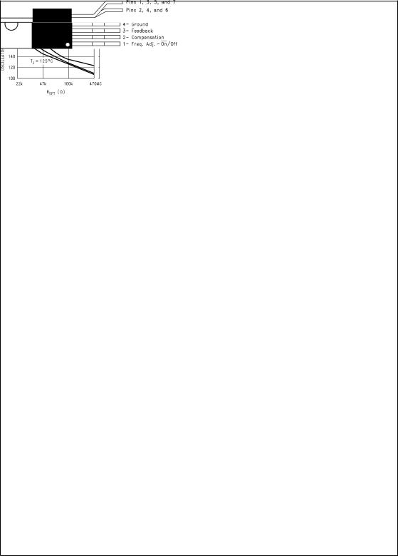
Note 10: When testing the minimum value, do not sink current from this pin Ð isolate it with a diode. If current is drawn from this pin, the frequency adjust circui t will begin operation (see Figure 41).
Note 11: Junction to ambient thermal resistance (no external heat sink) for the 7 lead TO-220 package mounted vertically, with 1¤2 inch leads in a socket, or on a PC board with minimum copper area.
Note 12: Junction to ambient thermal resistance (no external heat sink) for the 7 lead TO-220 package mounted vertically, with 1¤2 inch leads soldered to a PC board containing approximately 4 square inches of (1 oz.) copper area surrounding the leads.
Note 13: Junction to ambient thermal resistance for the 7 lead TO-263 mounted horizontally against a PC board area of 0.136 square inches (the same size as the TO-263 package) of 1 oz. (0.0014 in. thick) copper.
Note 14: Junction to ambient thermal resistance for the 7 lead TO-263 mounted horizontally against a PC board area of 0.4896 square inches (3.6 times the area of the TO-263 package) of 1 oz. (0.0014 in. thick) copper.
www.national.com |
6 |

All Output Voltage Versions
Electrical Characteristics (Note 5) (Continued)
Note 15: Junction to ambient thermal resistance for the 7 lead TO-263 mounted horizontally against a PC board copper area of 1.0064 square inches (7.4 times the area of the TO-263 package) of 1 oz. (0.0014 in. thick) copper. Additional copper area will reduce thermal resistance further. See the thermal model in Switchers Made Simple® software.
Typical Performance Characteristics
Supply Current |
Reference Voltage |
Reference Voltage |
vs Temperature |
vs Temperature |
vs Supply Voltage |
DS012420-2 DS012420-3 DS012420-4
Supply Current |
Current Limit |
Feedback Pin Bias |
vs Switch Current |
vs Temperature |
Current vs Temperature |
DS012420-5 |
DS012420-6 |
DS012420-7 |
|
|
Switch Saturation |
Switch Transconductance |
Oscillator Frequency |
Voltage vs Temperature |
vs Temperature |
vs Temperature |
DS012420-8 |
DS012420-9 |
DS012420-10 |
|
|
7 |
www.national.com |
Typical Performance Characteristics (Continued)
Error Amp Transconductance |
Error Amp Voltage |
Short Circuit Frequency |
vs Temperature |
Gain vs Temperature |
vs Temperature |
|
DS012420-11 |
|
DS012420-12 |
DS012420-13 |
Shutdown Supply Current |
|
|
|
|
|
ON /OFF Pin Current |
Oscillator Frequency |
||
vs Temperature |
|
vs Voltage |
vs Resistance |
|
DS012420-14 |
DS012420-15 |
DS012420-16 |
|
|
|
Connection Diagrams |
|
|
Bent, Staggered Leads |
|
Bent, Staggered Leads |
7-Lead TO-220 (T) |
|
|
|
7-Lead TO-220 (T) |
|
Top View |
|
|
|
Side View |
|
|
|
|
|
|
DS012420-18 |
|
DS012420-17 |
|
Order Number LM2588T-3.3, LM2588T-5.0,
LM2588T-12 or LM2588T-ADJ
See NS Package Number TA07B
www.national.com |
8 |
Connection Diagrams (Continued)
7-Lead TO-263 (S) |
7-Lead TO-263 (S) |
Top View |
Side View |
DS012420-20
DS012420-19
Order Number LM2588S-3.3, LM2588S-5.0,
LM2588S-12 or LM2588S-ADJ
Tape and Reel Order Number LM2588SX-3.3,
LM2588SX-5.0, LM2588SX-12 or LM2588SX-ADJ
See NS Package Number TS7B
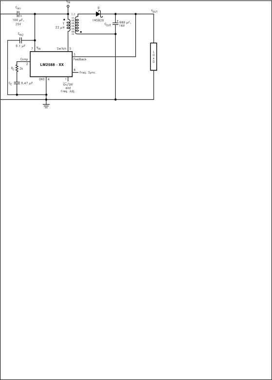
Test Circuits
DS012420-21
CIN1 Ð 100 µF, 25V Aluminum Electrolytic
CIN2 Ð 0.1 µF Ceramic
T Ð 22 µH, 1:1 Schott #67141450
D Ð 1N5820
COUT Ð 680 µF, 16V Aluminum Electrolytic
CC Ð 0.47 µF Ceramic
RC Ð 2k
FIGURE 1. LM2588-3.3 and LM2588-5.0
9 |
www.national.com |
 Loading...