


LM2587T-ADJ
NSC LM2587T-ADJ, LM2587T-5.0, LM2587T-12, LM2587SX-ADJ, LM2587SX-3.3 Datasheet
...
LM2587
SIMPLE SWITCHER
®
5A Flyback Regulator
General Description
The LM2587 series of regulators are monolithic integrated
circuits specifically designed for flyback, step-up (boost), and
forward converter applications. The device is available in 4
different output voltage versions: 3.3V, 5.0V,12V,andadjust-
able.
Requiring a minimum number of external components,these
regulators are cost effective, and simple to use. Included in
the datasheet are typical circuits of boostandflybackregula-
tors.Alsolistedare selector guides for diodes and capacitors
and a family of standard inductors and flyback transformers
designed to work with these switching regulators.
The power switch is a 5.0A NPN device that can stand-off
65V. Protecting the power switch are current and thermal
limiting circuits, and an undervoltage lockout circuit. This IC
contains a 100 kHz fixed-frequency internal oscillator that
permits the use of small magnetics. Other features include
soft start mode to reducein-rush current during start up, cur-
rent mode control forimproved rejection of input voltage and
output load transients and cycle-by-cycle current limiting.An
output voltage tolerance of
±
4
%
, within specified input volt-
ages and output load conditions, is guaranteedforthepower
supply system.
Features
n Requires few external components
n Family of standard inductors and transformers
n NPN output switches 5.0A, can stand off 65V
n Wide input voltage range: 4V to 40V
n Current-mode operation for improved transient
response, line regulation, and current limit
n 100 kHz switching frequency
n Internal soft-start function reduces in-rush current during
start-up
n Output transistor protected by current limit, under
voltage lockout, and thermal shutdown
n System Output Voltage Tolerance of
±
4
%
max over line
and load conditions
Typical Applications
n Flyback regulator
n Multiple-output regulator
n Simple boost regulator
n Forward converter
Flyback Regulator
Ordering Information
Package Type NSC Package Order Number
Drawing
5-Lead TO-220 Bent, Staggered Leads T05D LM2587T-3.3, LM2587T-5.0, LM2587T-12, LM2587T-ADJ
5-Lead TO-263 TS5B LM2587S-3.3, LM2587S-5.0, LM2587S-12, LM2587S-ADJ
5-Lead TO-263 Tape and Reel TS5B LM2587SX-3.3, LM2587SX-5.0, LM2587SX-12,
LM2587SX-ADJ
SIMPLE SWITCHER
®
and
Switchers Made Simple
®
are registered trademarks of National SemiconductorCorporation.
DS012316-1
April 1998
LM2587 SIMPLE SWITCHER 5A Flyback Regulator
© 1999 National Semiconductor Corporation DS012316 www.national.com
Absolute Maximum Ratings (Note 1)
If Military/Aerospace specified devices are required,
please contact the National Semiconductor Sales Office/
Distributors for availability and specifications.
Input Voltage −0.4V ≤ V
IN
≤ 45V
Switch Voltage −0.4V ≤ V
SW
≤ 65V
Switch Current (Note 2) Internally Limited
Compensation Pin Voltage −0.4V ≤ V
COMP
≤ 2.4V
Feedback Pin Voltage −0.4V ≤ V
FB
≤ 2V
OUT
Storage Temperature Range −65˚C to +150˚C
Lead Temperature
(Soldering, 10 sec.) 260˚C
Maximum Junction
Temperature (Note 3) 150˚C
Power Dissipation (Note 3) Internally Limited
Minimum ESD Rating
(C
=
100 pF, R
=
1.5 kΩ 2kV
Operating Ratings
Supply Voltage 4V ≤ V
IN
≤ 40V
Output Switch Voltage 0V ≤ V
SW
≤ 60V
Output Switch Current I
SW
≤ 5.0A
Junction Temperature Range −40˚C ≤ T
J
≤ +125˚C
LM2587-3.3
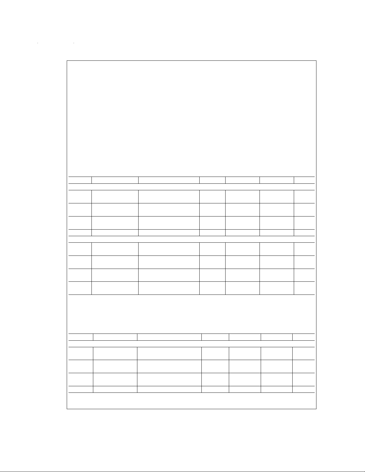
Electrical Characteristics
Specifications with standard type face are for T
J
=
25˚C, and those in bold type face apply over full Operating Temperature
Range. Unless otherwise specified, V
IN
=
5V.
Symbol Parameters Conditions Typical Min Max Units
SYSTEM PARAMETERS Test Circuit of
Figure 2
(Note 4)
V
OUT
Output Voltage V
IN
=
4V to 12V 3.3 3.17/3.14 3.43/3.46 V
I
LOAD
=
400 mA to 1.75A
∆V
OUT
/ Line Regulation V
IN
=
4V to 12V 20 50/100 mV
∆V
IN
I
LOAD
=
400 mA
∆V
OUT
/ Load Regulation V
IN
=
12V 20 50/100 mV
∆I
LOAD
I
LOAD
=
400 mA to 1.75A
η Efficiency V
IN
=
12V, I
LOAD
=
1A 75
%
UNIQUE DEVICE PARAMETERS (Note 5)
V
REF
Output Reference Measured at Feedback Pin 3.3 3.242/3.234 3.358/3.366 V
Voltage V
COMP
=
1.0V
∆V
REF
Reference Voltage V
IN
=
4V to 40V 2.0 mV
Line Regulation
G
M
Error Amp I
COMP
=
−30 µA to +30 µA 1.193 0.678 2.259 mmho
Transconductance V
COMP
=
1.0V
A
VOL
Error Amp V
COMP
=
0.5V to 1.6V 260 151/75 V/V
Voltage Gain R
COMP
=
1.0 MΩ (Note 6)
LM2587-5.0
Electrical Characteristics
Specifications with standard type face are for T
J
=
25˚C, and those in bold type face apply over full Operating Temperature
Range. Unless otherwise specified, V
IN
=
5V.
Symbol Parameters Conditions Typical Min Max Units
SYSTEM PARAMETERS Test Circuit of
Figure 2
(Note 4)
V
OUT
Output Voltage V
IN
=
4V to 12V 5.0 4.80/4.75 5.20/5.25 V
I
LOAD
=
500 mA to 1.45A
∆V
OUT
/ Line Regulation V
IN
=
4V to 12V 20 50/100 mV
∆V
IN
I
LOAD
=
500 mA
∆V
OUT
/ Load Regulation V
IN
=
12V 20 50/100 mV
∆I
LOAD
I
LOAD
=
500 mA to 1.45A
η Efficiency V
IN
=
12V, I
LOAD
=
750 mA 80
%
www.national.com 2
LM2587-5.0
Electrical Characteristics
(Continued)
Symbol Parameters Conditions Typical Min Max Units
UNIQUE DEVICE PARAMETERS (Note 5)
V
REF
Output Reference Measured at Feedback Pin 5.0 4.913/4.900 5.088/5.100 V
Voltage V
COMP
=
1.0V
∆V
REF
Reference Voltage V
IN
=
4V to 40V 3.3 mV
Line Regulation
G
M
Error Amp I
COMP
=
−30 µA to +30 µA 0.750 0.447 1.491 mmho
Transconductance V
COMP
=
1.0V
A
VOL
Error Amp V
COMP
=
0.5V to 1.6V 165 99/49 V/V
Voltage Gain R
COMP
=
1.0 MΩ (Note 6)
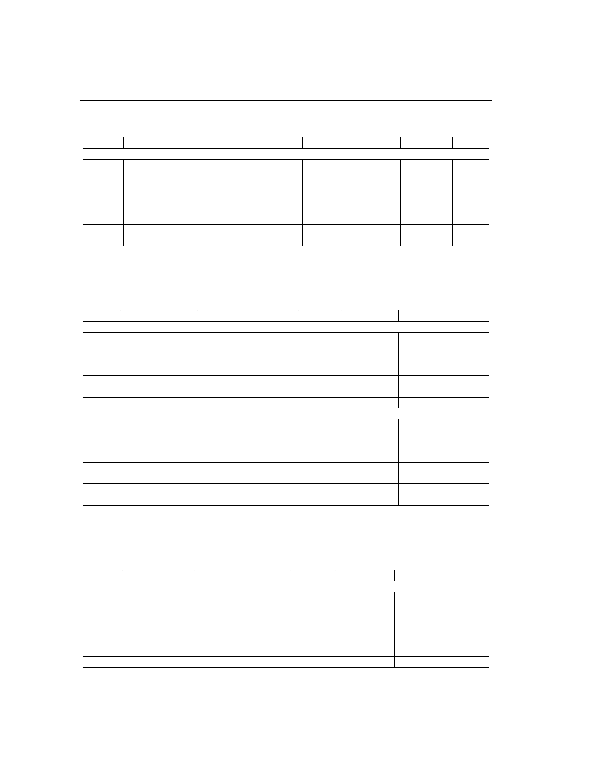
LM2587-12
Electrical Characteristics
Specifications with standard type face are for T
J
=
25˚C, and those in bold type face apply over full Operating Temperature
Range. Unless otherwise specified, V
IN
=
5V.
Symbol Parameters Conditions Typical Min Max Units
SYSTEM PARAMETERS Test Circuit of
Figure 3
(Note 4)
V
OUT
Output Voltage V
IN
=
4V to 10V 12.0 11.52/11.40 12.48/12.60 V
I
LOAD
=
300 mA to 1.2A
∆V
OUT
/ Line Regulation V
IN
=
4V to 10V 20 100/200 mV
∆V
IN
I
LOAD
=
300 mA
∆V
OUT
/ Load Regulation V
IN
=
10V 20 100/200 mV
∆I
LOAD
I
LOAD
=
300 mA to 1.2A
η Efficiency V
IN
=
10V, I
LOAD
=
1A 90
%
UNIQUE DEVICE PARAMETERS (Note 5)
V
REF
Output Reference Measured at Feedback Pin 12.0 11.79/11.76 12.21/12.24 V
Voltage V
COMP
=
1.0V
∆V
REF
Reference Voltage V
IN
=
4V to 40V 7.8 mV
Line Regulation
G
M
Error Amp I
COMP
=
−30 µA to +30 µA 0.328 0.186 0.621 mmho
Transconductance V
COMP
=
1.0V
A
VOL
Error Amp V
COMP
=
0.5V to 1.6V 70 41/21 V/V
Voltage Gain R
COMP
=
1.0 MΩ (Note 6)
LM2587-ADJ
Electrical Characteristics
Specifications with standard type face are for T
J
=
25˚C, and those in bold type face apply over full Operating Temperature
Range. Unless otherwise specified, V
IN
=
5V.
Symbol Parameters Conditions Typical Min Max Units
SYSTEM PARAMETERS Test Circuit of
Figure 3
(Note 4)
V
OUT
Output Voltage V
IN
=
4V to 10V 12.0 11.52/11.40 12.48/12.60 V
I
LOAD
=
300 mA to 1.2A
∆V
OUT
/ Line Regulation V
IN
=
4V to 10V 20 100/200 mV
∆V
IN
I
LOAD
=
300 mA
∆V
OUT
/ Load Regulation V
IN
=
10V 20 100/200 mV
∆I
LOAD
I
LOAD
=
300 mA to 1.2A
η Efficiency V
IN
=
10V, I
LOAD
=
1A 90
%
www.national.com3
LM2587-ADJ
Electrical Characteristics
(Continued)
Symbol Parameters Conditions Typical Min Max Units
UNIQUE DEVICE PARAMETERS (Note 5)
V
REF
Output Reference Measured at Feedback Pin 1.230 1.208/1.205 1.252/1.255 V
Voltage V
COMP
=
1.0V
∆V
REF
Reference Voltage V
IN
=
4V to 40V 1.5 mV
Line Regulation
G
M
Error Amp I
COMP
=
−30 µA to +30 µA 3.200 1.800 6.000 mmho
Transconductance V
COMP
=
1.0V
A
VOL
Error Amp V
COMP
=
0.5V to 1.6V 670 400/200 V/V
Voltage Gain R
COMP
=
1.0 MΩ (Note 6)
I
B
Error Amp V
COMP
=
1.0V 125 425/600 nA
Input Bias Current
All Output Voltage Versions
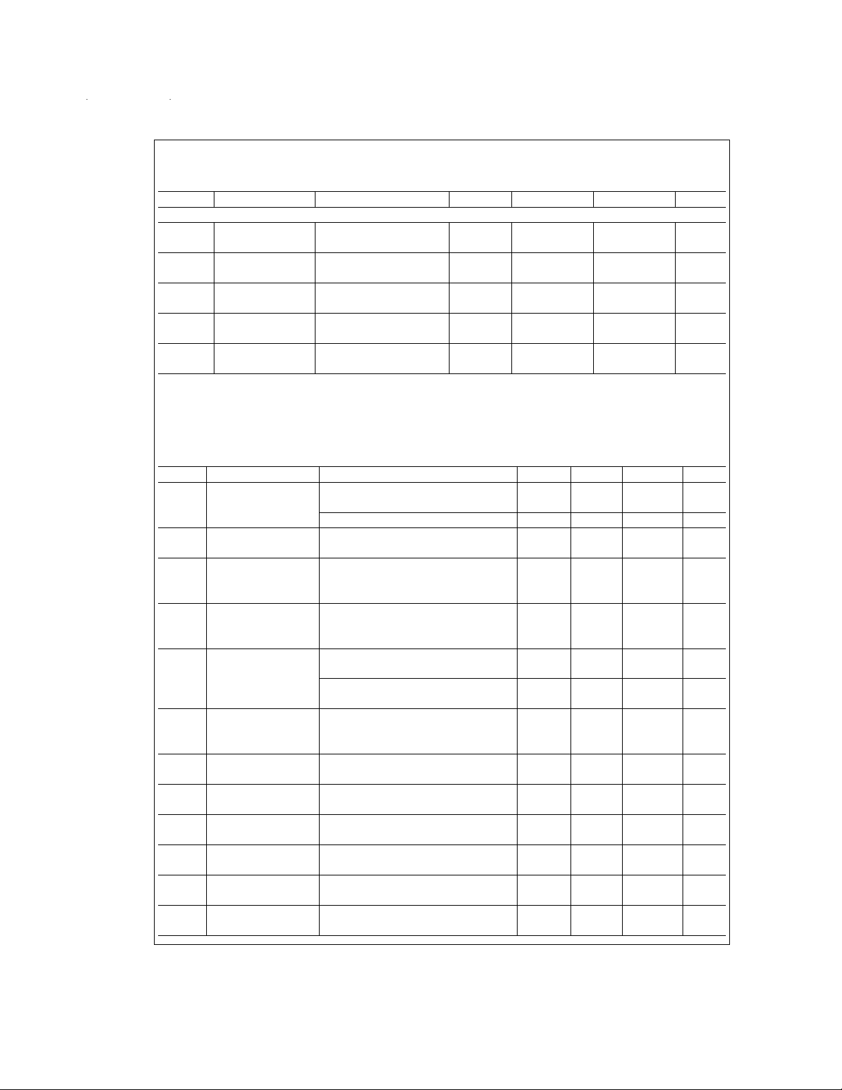
Electrical Characteristics
(Note 5)
Specifications with standard type face are for T
J
=
25˚C, and those in bold type face apply over full Operating Temperature
Range. Unless otherwise specified, V
IN
=
5V.
Symbol Parameters Conditions Typical Min Max Units
I
S
Input Supply Current (Switch Off) 11 15.5/16.5 mA
(Note 8)
I
SWITCH
=
3.0A 85 140 165 mA
V
UV
Input Supply R
LOAD
=
100Ω 3.30 3.05 3.75 V
Undervoltage Lockout
f
O
Oscillator Frequency Measured at Switch Pin
R
LOAD
=
100Ω 100 85/75 115/125 kHz
V
COMP
=
1.0V
f
SC
Short-Circuit Measured at Switch Pin
Frequency R
LOAD
=
100Ω 25 kHz
V
FEEDBACK
=
1.15V
V
EAO
Error Amplifier Upper Limit 2.8 2.6/2.4 V
Output Swing (Note 7)
Lower Limit 0.25 0.40/0.55 V
(Note 8)
I
EAO
Error Amp (Note 9)
Output Current 165 110/70 260/320 µA
(Source or Sink)
I
SS
Soft Start Current V
FEEDBACK
=
0.92V 11.0 8.0/7.0 17.0/19.0 µA
V
COMP
=
1.0V
D Maximum Duty Cycle R
LOAD
=
100Ω 98 93/90
%
(Note 7)
I
L
Switch Leakage Switch Off 15 300/600 µA
Current V
SWITCH
=
60V
V
SUS
Switch Sustaining dV/dT
=
1.5V/ns 65 V
Voltage
V
SAT
Switch Saturation I
SWITCH
=
5.0A 0.7 1.1/1.4 V
Voltage
I
CL
NPN Switch 6.5 5.0 9.5 A
Current Limit
www.national.com 4
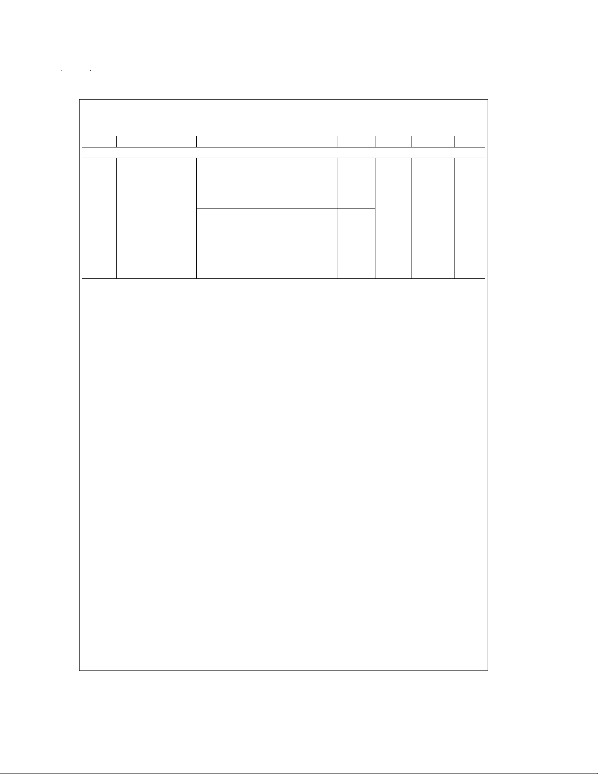
All Output Voltage Versions
Electrical Characteristics
(Note 5) (Continued)
Symbol Parameters Conditions Typical Min Max Units
COMMON DEVICE PARAMETERS (Note 4)
θ
JA
Thermal Resistance T Package, Junction to Ambient
(Note 10)
65
θ
JA
T Package, Junction to Ambient
(Note 11)
45
θ
JC
T Package, Junction to Case 2
θ
JA
S Package, Junction to Ambient
(Note 12)
56
˚C/W
θ
JA
S Package, Junction to Ambient
(Note 13)
35
θ
JA
S Package, Junction to Ambient
(Note 14)
26
θ
JC
S Package, Junction to Case 2
Note 1: Absolute Maximum Ratings indicate limits beyond which damage to the device may occur. Operating ratings indicate conditions the device is intended to
be functional, but device parameter specifications may not be guaranteed under these conditions. For guaranteed specifications and test conditions, see the Electrical
Characteristics.
Note 2: Note that switch current and output current are not identical in a step-up regulator. Output current cannot be internally limited when the LM2587 is used as
a step-up regulator. To prevent damage to the switch, the output current must be externally limited to 5A. However, output current is internally limited when the
LM2587 is used as a flyback regulator (see the Application Hints section for more information).
Note 3: The junction temperature of the device (T
J
) is a function of the ambient temperature (T
A
), the junction-to-ambient thermal resistance (θ
JA
), and the power
dissipation of the device (P
D
). A thermal shutdown will occur if the temperature exceedsthe maximum junction temperature of the device: P
D
x θ
JA
+T
A(MAX)
≥ T
J
-
(MAX)
. For a safe thermal design, check that the maximum power dissipated by the device is less than: P
D
≤ [T
J(MAX)
−T
A(MAX)
)]/θ
JA
. When calculating the maximum
allowable power dissipation, derate the maximum junction temperature — this ensures a margin of safety in the thermal design.
Note 4: External components such as the diode, inductor, input and output capacitors can affect switching regulator performance. When the LM2587 is used as
shown in
Figure 2
and
Figure 3
, system performance will be as specified by the system parameters.
Note 5: All room temperature limits are 100
%
production tested, and all limits at temperature extremes are guaranteed via correlation using standard Statistical Qual-
ity Control (SQC) methods.
Note 6: A 1.0 MΩ resistor is connected to the compensation pin (which is the error amplifier output) to ensure accuracy in measuringA
VOL
.
Note 7: Tomeasure this parameter, the feedback voltage is set to a low value, depending on the output version of the device, to force the error amplifier output high.
Adj: V
FB
=
1.05V; 3.3V: V
FB
=
2.81V; 5.0V: V
FB
=
4.25V; 12V: V
FB
=
10.20V.
Note 8: Tomeasure this parameter, the feedback voltage is set to a high value, depending on the output version of the device, to force the error amplifier output low.
Adj: V
FB
=
1.41V; 3.3V: V
FB
=
3.80V; 5.0V: V
FB
=
5.75V; 12V: V
FB
=
13.80V.
Note 9: Tomeasure the worst-case error amplifier output current, the LM2587 is tested with the feedback voltage set to its low value (specified in Note 7) and at its
high value (specified in Note 8).
Note 10: Junction to ambient thermal resistance (no external heat sink) for the 5 lead TO-220 package mounted vertically,with
1
⁄
2
inch leads in a socket, or on a PC
board with minimum copper area.
Note 11: Junction to ambient thermal resistance (no external heat sink) for the 5 lead TO-220 package mounted vertically,with
1
⁄
2
inch leads soldered to a PC board
containing approximately 4 square inches of (1oz.) copper area surrounding the leads.
Note 12: Junction to ambient thermal resistance for the 5 lead TO-263 mounted horizontally against a PC board area of 0.136 square inches (the same size as the
TO-263 package) of 1 oz. (0.0014 in. thick) copper.
Note 13: Junction to ambient thermal resistance for the 5 leadTO-263 mounted horizontally against a PC board areaof 0.4896 square inches (3.6 times the area
of the TO-263 package) of 1 oz. (0.0014 in. thick) copper.
Note 14: Junction to ambient thermal resistance for the 5 lead TO-263 mounted horizontally against a PC board copper area of 1.0064 square inches (7.4 times the
area of the TO-263 package) of 1 oz. (0.0014 in. thick) copper.Additional copper area will reduce thermal resistance further. See the thermal model in Switchers Made
Simple
®
software.
www.national.com5
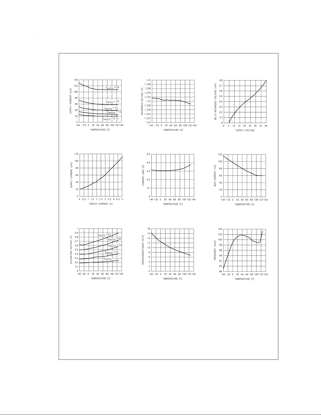
Typical Performance Characteristics
Supply Current
vs Temperature
DS012316-48
Reference Voltage
vs Temperature
DS012316-49
∆Reference Voltage
vs Supply Voltage
DS012316-50
Supply Current
vs Switch Current
DS012316-51
Current Limit
vs Temperature
DS012316-52
Feedback Pin Bias
Current vs Temperature
DS012316-53
Switch Saturation
Voltage vs Temperature
DS012316-54
Switch Transconductance
vs Temperature
DS012316-55
Oscillator Frequency
vs Temperature
DS012316-56
www.national.com 6
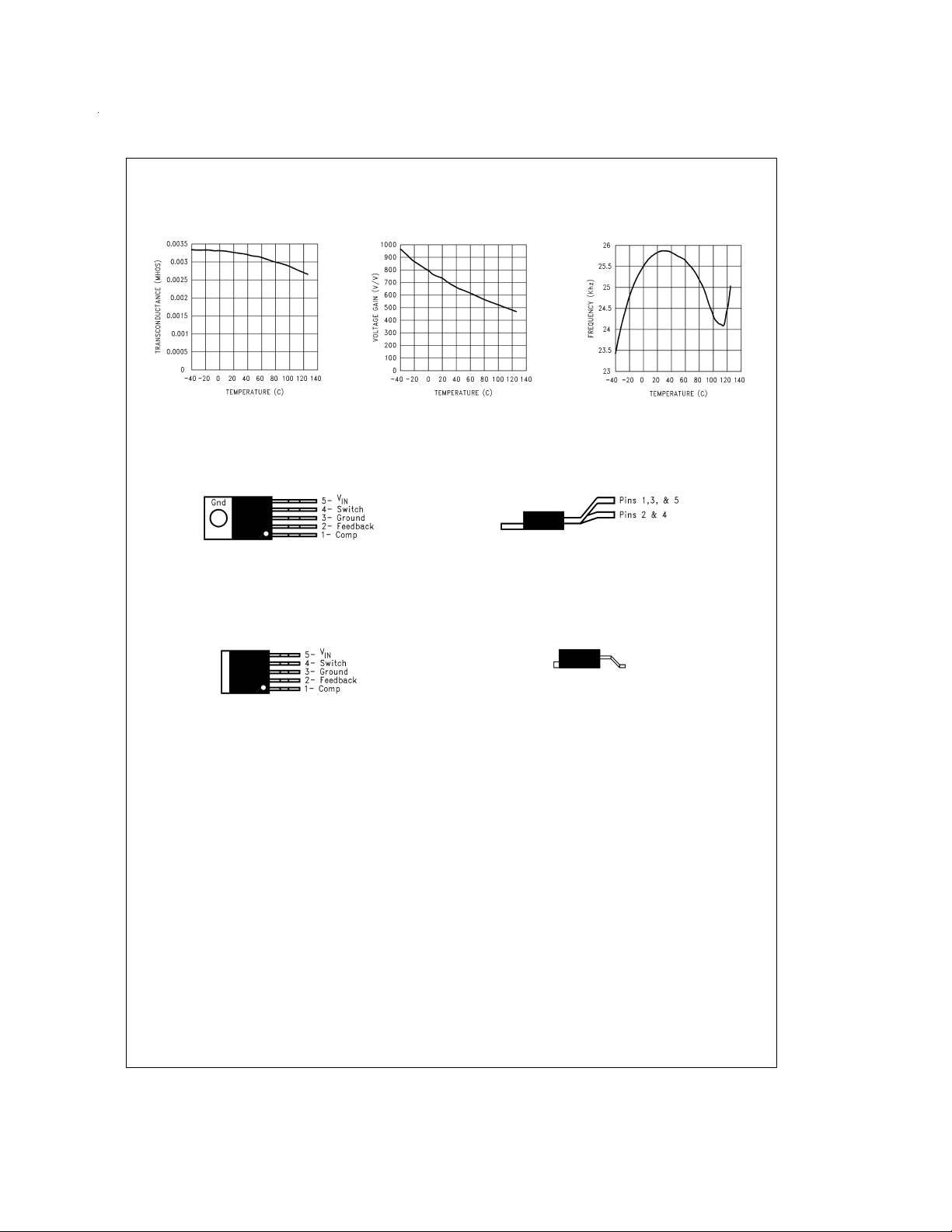
Typical Performance Characteristics (Continued)
Connection Diagrams
Error Amp Transconductance
vs Temperature
DS012316-57
Error Amp Voltage
Gain vs Temperature
DS012316-58
Short Circuit Frequency
vs Temperature
DS012316-59
Bent, Staggered Leads
5-Lead TO-220 (T)
Top View
DS012316-3
Bent, Staggered Leads
5-Lead TO-220 (T)
Side View
DS012316-4
Order Number LM2587T-3.3, LM2587T-5.0,
LM2587T-12 or LM2587T-ADJ
See NS Package Number T05D
5-Lead TO-263 (S)
Top View
DS012316-5
5-Lead TO-263 (S)
Side View
DS012316-6
Order Number LM2587S-3.3, LM2587S-5.0,
LM2587S-12 or LM2587S-ADJ
See NS Package Number TS5B
www.national.com7
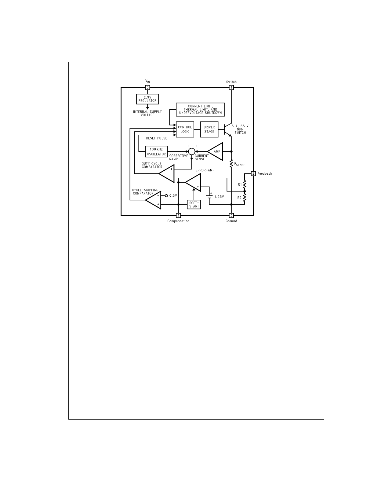
Block Diagram
DS012316-7
For Fixed Versions
3.3V, R1
=
3.4k, R2
=
2k
5V, R1
=
6.15k, R2
=
2k
12V, R1
=
8.73k, R2
=
1k
For Adj. Version
R1
=
Short (0Ω), R2
=
Open
FIGURE 1.
www.national.com 8
 Loading...