


Mitsubishi M5M5V408BTP-85LW, M5M5V408BTP-10HW, M5M5V408BTP-10HI, M5M5V408BTP-10H, M5M5V408BRT-85LW Datasheet
...revision-K1.0e, ' 98.09.07
M5M5V408BFP/TP/RT/KV/KR
MITSUBISHI LSIs
4194304-BIT (524288-WORD BY 8-BIT) CMOS STATIC RAM
DESCRIPTION |
FEATURES |
The M5M5V408B is a family of low voltage 4-Mbit static RAMs organized as 524,288-words by 8-bit, fabricated by Mitsubishi's highperformance 0.25µm CMOS technology.
The M5M5V408B is suitable for memory applications where a simple interfacing , battery operating and battery backup are the important design objectives.
M5M5V408B is packaged in 32-pin plastic SOP, 32-pin plastic TSOP and 32-pin 8mm x 13.4mm STSOP packages. Two types of TSOPs and two types of STSOPs are available, M5M5V408BTP (normal-lead-bend TSOP), M5M5V408BRT (reverse-lead-bend TSOP), M5M5V408BKV (normal-lead-bend STSOP) and M5M5V408BKR (reverse-lead-bend STSOP). These two types TSOPs and two types STSOPs are suitable for a surface mounting on double-sided printed circuit boards.
From the point of operating temperature, the family is divided into three versions; "Standard", "W-version", and "I-version". Those are summarized in the part name table below.
•Single +2.7~+3.6V power supply
•Small stand-by current: 0.3µA(3V,typ.)
• No clocks, No refresh
• Data retention supply voltage=2.0V to 3.6V
• All inputs and outputs are |
TTL |
compatible. |
||||
• Easy memory expansion by |
|
S |
|
|
||
• Common Data I/O |
|
|
|
|
||
• Three-state outputs: OR-tie |
|
capability |
||||
• |
|
prevents data contention in |
the I/O bus |
|||
OE |
||||||
•Process technology: 0.25µm CMOS
•Package:
M5M5V408BFP: 32 pin 525 mil SOP M5M5V408BTP/RT: 32 PIN 400mil TSOP(ll) M5M5V408BKV/KR: 32 pin 8mm x13.4mm STSOP
PART NAME TABLE
Version, |
Part name |
Power |
Access |
Stand-by current Icc(PD), Vcc=3.0V |
Active |
||||||
current |
|||||||||||
Operating |
(## stands for "FP","TP", |
time |
typical * |
Ratings (max.) |
|
||||||
Supply |
|
Icc1 |
|||||||||
temperature |
"RT","KV"or"KR") |
max. |
25°C |
40°C |
25°C |
40°C |
70°C |
85°C |
|||
|
(3.0V, typ.) |
||||||||||
|
M5M5V408B## -85L |
2.7 ~ 3.6V |
85ns |
--- |
--- |
--- |
--- |
20µA |
--- |
|
|
Standard |
M5M5V408B## -10L |
100ns |
|
||||||||
|
|
|
|
|
|
|
|
||||
0 ~ +70°C |
M5M5V408B## -85H |
2.7 ~ 3.6V |
85ns |
0.3µA |
1µA |
1µA |
3µA |
10µA |
--- |
|
|
|
M5M5V408B## -10H |
100ns |
30mA |
||||||||
|
|
|
|
|
|
|
|
||||
|
M5M5V408B## -85LW |
|
85ns |
|
|
|
|
|
|
||
|
2.7 ~ 3.6V |
--- |
--- |
--- |
--- |
20µA |
40µA |
(10MHz) |
|||
W-version |
M5M5V408B## -10LW |
100ns |
|||||||||
|
|
|
|
|
|
||||||
|
|
|
|
|
|
|
|
||||
-20 ~ +85°C |
M5M5V408B## -85HW |
2.7 ~ 3.6V |
85ns |
0.3µA |
1µA |
1µA |
3µA |
10µA |
20µA |
5mA |
|
|
M5M5V408B## -10HW |
100ns |
(1MHz) |
||||||||
|
|
|
|
|
|
|
|
||||
|
M5M5V408B## -85LI |
2.7 ~ 3.6V |
85ns |
--- |
--- |
--- |
--- |
|
|
|
|
|
|
|
20µA |
40µA |
|
||||||
I-version |
M5M5V408B## -10LI |
100ns |
|
||||||||
|
|
|
|
|
|
||||||
|
|
|
|
|
|
|
|
||||
-40 ~ +85°C |
M5M5V408B## -85HI |
2.7 ~ 3.6V |
85ns |
0.3µA |
1µA |
1µA |
3µA |
10µA |
20µA |
|
|
|
M5M5V408B## -10HI |
100ns |
|
||||||||
|
|
|
|
|
|
|
|
|
|||
* "typical" parameter is sampled, not 100% tested.
MITSUBISHI ELECTRIC |
1 |
|
revision-K1.0e, ' 98.09.07
M5M5V408BFP/TP/RT/KV/KR
MITSUBISHI LSIs
4194304-BIT (524288-WORD BY 8-BIT) CMOS STATIC RAM
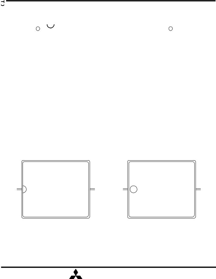
PIN CONFIGURATION (TOP VIEW)
A18 |
|
|
|
|
VCC |
VCC |
|
|
|
|
|
A18 |
|||||||||
|
1 |
|
32 |
|
32 |
|
1 |
||||||||||||||
A16 |
|
|
|
|
|
A15 |
A15 |
|
|
|
|
A16 |
|||||||||
|
2 |
|
31 |
|
|
31 |
|
2 |
|||||||||||||
A14 |
|
|
|
|
|
A17 |
A17 |
|
|
|
|
|
A14 |
||||||||
|
3 |
|
30 |
|
30 |
|
3 |
||||||||||||||
A12 |
|
|
|
|
|
|
|
|
|
|
|
|
|
|
|
|
A12 |
||||
|
4 |
|
29 |
|
W |
|
|
W |
|
29 |
|
|
4 |
||||||||
|
|
|
|
|
|
|
|
|
|
|
|
|
|
|
|
|
|
||||
A7 |
|
|
|
|
A13 |
A13 |
|
|
|
|
|
A7 |
|||||||||
|
5 |
|
28 |
|
28 |
|
5 |
||||||||||||||
A6 |
|
|
|
|
|
A8 |
|
A8 |
|
|
|
|
|
A6 |
|||||||
|
6 |
|
27 |
|
27 |
|
|
6 |
|||||||||||||
A5 |
|
|
|
|
|
A9 |
|
A9 |
|
|
|
|
|
A5 |
|||||||
|
7 |
|
26 |
|
26 |
|
7 |
||||||||||||||
A4 |
|
|
|
|
|
A11 |
A11 |
|
|
|
|
|
A4 |
||||||||
|
8 |
|
25 |
|
|
25 |
|
|
8 |
||||||||||||
A3 |
|
|
|
|
|
|
|
|
|
|
|
|
|
|
|
|
|
|
|
|
A3 |
|
9 |
|
24 |
OE |
OE |
|
24 |
|
|
9 |
|||||||||||
|
|
|
|
|
|
|
|
|
|
||||||||||||
A2 |
|
|
|
|
|
A10 |
A10 |
|
|
|
|
|
A2 |
||||||||
|
10 |
|
23 |
|
|
23 |
|
|
10 |
||||||||||||
|
|
|
|
|
|
|
|||||||||||||||
|
|
|
|
|
|
|
|
|
|
|
|
|
|
|
|
|
|
|
|
|
|
A1 |
|
11 |
|
22 |
S |
|
|
S |
|
22 |
|
|
11 |
A1 |
|||||||
|
|
|
|
|
|
|
|
|
|
|
|||||||||||
A0 |
|
|
|
|
|
DQ8 |
DQ8 |
|
|
|
|
|
A0 |
||||||||
|
|
12 |
|
21 |
|
|
|
|
|
|
|
|
|
|
|
|
21 |
|
|
|
|
DQ1 |
|
|
|
|
|
DQ7 |
DQ7 |
|
|
|
|
|
DQ1 |
||||||||
|
|
|
|
|
20 |
|
|
13 |
|||||||||||||
DQ2 |
|
13 |
|
20 |
|
DQ6 |
DQ6 |
|
|
|
|
|
DQ2 |
||||||||
|
|
|
|
|
|
|
|
|
|
||||||||||||
|
|
|
|
|
|
|
|
|
|
||||||||||||
|
14 |
|
19 |
|
|
19 |
|
|
14 |
||||||||||||
DQ3 |
|
|
|
|
|
DQ5 |
DQ5 |
|
|
|
|
|
DQ3 |
||||||||
|
15 |
|
18 |
|
|
18 |
|
|
15 |
||||||||||||
|
|
|
|
|
|
|
|||||||||||||||
GND |
|
|
|
|
|
DQ4 |
DQ4 |
17 |
|
|
16 |
GND |
|||||||||
|
|
16 |
|
17 |
|
|
|
|
|
|
|
|
|
|
|
|
|
|
|
|
|
|
|
|
|
|
|
|
|
|
|
|
|
|
|
|
|
|
|
|
|
|
|
|
|
|
|
|
|
|
|
|
|
|
|
|
|
|
|
|
|
|
|
|
|
|
|
|
|
|
|
|
|
|
|
|
|
|
|
|
|
|
|
|
|
|
|
|
Outline 32P2M-A (FP) |
|
|
|
|
|
|
|
|
|
|
|
|
Outline |
32P3Y-J (RT) |
|
|||||
|
|
|
32P3Y-H (TP) |
|
|
|
|
|
|
|
|
|
|
|
|
|
|
|
|
|
|
|
A11 |
|
|
|
|
|
OE |
|
A4 |
|
|
|
|
|
A3 |
|
|
|
1 |
|
32 |
|
|
|
16 |
|
17 |
|
|||||
|
A9 |
|
|
|
|
A10 |
A5 |
|
|
|
|
A2 |
||||
|
|
2 |
|
31 |
|
|
15 |
|
18 |
|
||||||
|
A8 |
|
|
|
|
|
S |
A6 |
|
|
|
|
A1 |
|||
|
|
3 |
|
30 |
|
|
14 |
|
19 |
|
||||||
|
A13 |
|
4 |
|
29 |
|
DQ8 |
A7 |
|
13 |
|
20 |
|
A0 |
||
|
|
|
|
|
|
|
DQ7 |
A12 |
|
|
|
|
DQ1 |
|||
|
W |
|
|
5 |
|
28 |
|
|
12 |
|
21 |
|
||||
|
A18 |
|
|
|
|
DQ6 |
A14 |
|
|
|
|
DQ2 |
||||
|
|
6 |
|
27 |
|
|
11 |
|
22 |
|
||||||
|
|
|
|
|
|
|
|
|
||||||||
|
A15 |
|
7 |
|
26 |
|
DQ5 |
A16 |
|
10 |
|
23 |
|
DQ3 |
||
|
Vcc |
|
|
|
|
DQ4 |
A17 |
|
|
|
|
|
GND |
|||
|
|
8 |
M5M5V408BKV |
25 |
|
|
9 |
M5M5V408BKR |
24 |
|
||||||
|
A17 |
|
9 |
24 |
|
GND |
Vcc |
|
8 |
25 |
|
DQ4 |
||||
|
|
|
|
|
||||||||||||
|
A16 |
|
10 |
|
23 |
|
DQ3 |
A15 |
|
7 |
|
26 |
|
DQ5 |
||
|
A14 |
|
|
|
|
DQ2 |
A18 |
|
|
|
|
DQ6 |
||||
|
|
11 |
|
22 |
|
|
6 |
|
27 |
|
||||||
|
A12 |
|
|
|
|
DQ1 |
W |
|
|
|
|
DQ7 |
||||
|
|
12 |
|
21 |
|
|
5 |
|
28 |
|
||||||
|
A7 |
|
|
|
|
A0 |
A13 |
|
|
|
|
|
DQ8 |
|||
|
|
13 |
|
20 |
|
|
4 |
|
29 |
|
||||||
|
A6 |
|
|
|
|
A1 |
A8 |
|
|
|
|
S |
||||
|
|
14 |
|
19 |
|
|
3 |
|
30 |
|
||||||
|
|
|
|
|
|
|
|
|
||||||||
|
A5 |
|
15 |
|
18 |
|
A2 |
A9 |
|
2 |
|
31 |
|
A10 |
||
|
|
|
|
|
|
|
|
|
||||||||
|
A4 |
|
16 |
|
17 |
|
A3 |
A11 |
|
1 |
|
32 |
|
OE |
||
|
|
Outline 32P3K-B |
|
|
|
Outline 32P3K-C |
|
|
||||||||
|
|
|
|
|
|
|
|
|
|
|
|
|
|
|
||
MITSUBISHI ELECTRIC |
2 |

revision-K1.0e, ' 98.09.07
M5M5V408BFP/TP/RT/KV/KR
MITSUBISHI LSIs
4194304-BIT (524288-WORD BY 8-BIT) CMOS STATIC RAM
FUNCTION
The M5M5408BFP,TP,RT,KV,KR is organized as 524,288words by 8-bit. These devices operate on a single +2.7~3.6V power supply, and are directly TTL compatible to both input and output. Its fully static circuit needs no clocks and no refresh, and makes it useful.
A write operation is executed during the S low and W low overlap time. The address(A0~A18) must be set up before the write cycle
A read operation is executed by setting W at a high level and OE at a low level while S are in an active state(S=L).
When setting S at a high level, the chips are in a nonselectable mode in which both reading and writing are disabled. In this mode, the output stage is in a high-impedance state, allowing OR-tie with other chips. Setting the OE at a high level,the output stage is in a high-impedance state, and the data bus contention problem in the write cycle is eliminated.
The power supply current is reduced as low as 0.3µA(25°C, typical), and the memory data can be held at +2V power supply, enabling battery back-up operation during power failure or power-down operation in the non-selected mode.
FUNCTION TABLE
|
|
|
|
|
|
|
|
|
Mode |
DQ |
Icc |
|
S |
|
W |
|
OE |
|
|||||
|
|
|
|
|
|
|
|
|
|
||
|
H |
|
X |
|
X |
|
Non selection |
High-impedance |
Standby |
||
|
L |
|
L |
|
X |
|
Write |
Data input (D) |
Active |
||
|
L |
|
H |
|
L |
|
Read |
Data output (Q) |
Active |
||
|
L |
|
H |
|
H |
|
Read |
High-impedance |
Active |
||
BLOCK DIAGRAM
Pin |
Function |
||
|
|
|
|
A0 ~ A18 |
Address input |
||
|
|
|
|
DQ1 ~ DQ8 |
Data input / output |
||
|
|
|
|
|
|
|
Chip select input |
|
S |
||
|
|
||
|
|
|
Write control input |
|
W |
||
|
|
||
|
Output inable input |
||
|
OE |
|
|
Vcc |
Power supply |
||
|
|
|
|
GND |
Ground supply |
||
|
|
|
|
M5M5V408B |
|
M5M5V408BKV/KR |
|
|
M5M5V408B |
|||
FP/TP/RT |
|
|
M5M5V408BKV/KR |
|||||
|
|
|
||||||
A4 |
8 |
16 |
|
|
|
FP/TP/RT |
||
|
|
|
|
|
||||
A5 |
7 |
15 |
|
|
21 |
13 |
DQ1 |
|
A6 |
6 |
14 |
|
|
22 |
14 |
DQ2 |
|
A7 |
5 |
13 |
MEMORY ARRAY |
23 |
15 |
DQ3 |
||
A12 |
4 |
12 |
25 |
17 |
DQ4 |
|||
|
|
|||||||
A14 |
3 |
11 |
524288 |
WORDS |
26 |
18 |
DQ5 |
|
A16 |
2 |
10 |
x 8 |
BITS |
27 |
19 |
DQ6 |
|
|
|
|||||||
A17 |
30 |
9 |
|
|
28 |
20 |
DQ7 |
|
A18 |
1 |
6 |
|
|
29 |
21 |
DQ8 |
|
A15 |
31 |
7 |
|
|
|
|
|
|
A10 |
23 |
31 |
|
|
|
|
|
|
A11 |
25 |
1 |
|
CLOCK |
|
|
|
|
A9 |
26 |
2 |
GENERATOR |
|
|
|
||
|
|
|
|
|
||||
A8 |
27 |
3 |
|
|
|
|
|
|
A13 |
28 |
4 |
|
|
5 |
29 |
W |
|
|
|
|
|
|
|
|
||
|
|
|
|
|
30 |
22 |
S |
|
|
|
|
|
|
|
|
||
A0 |
12 |
20 |
|
|
32 |
24 |
OE |
|
A1 |
11 |
19 |
|
|
|
|
|
|
A2 |
10 |
18 |
|
|
8 |
32 |
VCC |
|
A3 |
9 |
17 |
|
|
|
|
(3V) |
|
|
|
|
|
GND |
||||
|
|
|
|
|
24 |
16 |
||
|
|
|
|
|
|
|
(0V) |
|
MITSUBISHI ELECTRIC |
3 |
revision-K1.0e, ' 98.09.07
M5M5V408BFP/TP/RT/KV/KR
MITSUBISHI LSIs
4194304-BIT (524288-WORD BY 8-BIT) CMOS STATIC RAM
ABSOLUTE MAXIMUM RATINGS
|
Symbol |
|
Parameter |
|
|
|
|
|
|
|
Conditions |
|
|
|
Ratings |
|
|
Units |
|
|
|||||||
|
|
|
|
|
|
|
|
|
|
|
|
|
|
|
|
|
|
|
|
|
|
|
|
||||
|
Vcc |
|
|
Supply voltage |
|
|
|
|
With respect to GND |
|
|
|
-0.5* ~ +4.6 |
|
|
V |
|
|
|||||||||
|
VI |
|
|
Input voltage |
|
|
|
|
With respect to GND |
|
-0.5* ~ Vcc + 0.5 |
|
|
|
|||||||||||||
|
|
|
|
|
|
|
|
|
|
|
|
|
|
|
|
|
|
|
|
|
|
|
|
||||
|
VO |
|
|
Output voltage |
|
|
|
|
With respect to GND |
|
|
|
0 ~ Vcc |
|
|
|
|
|
|||||||||
|
|
|
|
|
|
|
|
|
|
|
|
|
|
|
|
|
|
|
|
|
|
|
|
|
|||
|
Pd |
|
|
Power dissipation |
|
|
|
|
|
|
Ta=25°C |
|
|
|
|
|
700 |
|
|
|
mW |
|
|
||||
|
|
|
|
Operating |
|
|
|
|
|
|
Standard |
(-L, -H) |
|
|
|
0 ~ +70 |
|
|
|
|
|
|
|||||
|
Ta |
|
|
|
|
|
|
|
|
W-version |
(-LW, -HW) |
|
|
|
-20 ~ +85 |
|
|
|
°C |
|
|
||||||
|
|
|
temperature |
|
|
|
|
|
|
|
|
|
|
|
|
|
|
||||||||||
|
|
|
|
|
|
|
|
|
|
I-version |
|
|
(-LI, -HI) |
|
|
|
-40 ~ +85 |
|
|
|
|
|
|
||||
|
|
|
|
|
|
|
|
|
|
|
|
|
|
|
|
|
|
|
|
|
|
||||||
|
Tstg |
|
|
Storage temperature |
|
|
|
|
|
|
|
|
|
|
|
|
|
|
|
|
-65 ~150 |
|
|
|
°C |
|
|
|
|
|
|
|
|
|
|
|
|
|
|
|
|
|
|
|
|
|
|
|
|
|
|
|
|||
|
|
|
|
|
|
|
|
|
|
|
|
|
|
|
|
|
* -3.0V in case of AC (Pulse width £ 30ns) |
|
|
||||||||
DC ELECTRICAL CHARACTERISTICS |
( Vcc=2.7 ~ 3.6V, unless otherwise noted) |
|
|||||||||||||||||||||||||
|
|
|
|
|
|
|
|
|
|
|
|
|
|
|
|
|
|
|
|
|
|
|
|
|
|
|
|
|
Symbol |
|
|
Parameter |
|
|
|
|
|
|
|
|
|
|
Conditions |
|
|
|
|
|
|
|
Limits |
|
Units |
||
|
|
|
|
|
|
|
|
|
|
|
|
|
|
|
|
|
|
|
|
|
|
||||||
|
|
|
|
|
|
|
|
|
|
|
|
|
|
|
|
|
|
Min |
Typ |
Max |
|||||||
|
|
|
|
|
|
|
|
|
|
|
|
|
|
|
|
|
|
|
|
|
|
|
|
||||
|
|
|
|
|
|
|
|
|
|
|
|
|
|
|
|
|
|
|
|
|
|
|
|
||||
|
VIH |
High-level input voltage |
|
|
|
|
|
|
|
|
|
|
|
|
|
|
|
|
|
2.2 |
|
Vcc+0.3V |
|
||||
|
VIL |
Low-level input voltage |
|
|
|
|
|
|
|
|
|
|
|
|
|
|
|
|
|
-0.3 * |
|
0.6 |
|
||||
|
VOH1 |
High-level output voltage 1 |
|
|
|
IOH= -0.5mA |
|
|
|
|
|
|
|
2.4 |
|
|
V |
||||||||||
|
VOH2 |
High-level output voltage 2 |
|
|
IOH= -0.05mA |
|
|
|
|
|
|
|
Vcc-0.5V |
|
|
|
|||||||||||
|
VOL |
Low-level output voltage |
|
|
IOL=2mA |
|
|
|
|
|
|
|
|
|
|
|
|
0.4 |
|
||||||||
|
II |
Input leakage current |
|
|
VI =0 ~ Vcc |
|
|
|
|
|
|
|
|
|
|
±1 |
µA |
||||||||||
|
IO |
Output leakage current |
|
|
|
|
|
|
|
|
|
|
|
|
|
|
|
|
|
|
|
|
±1 |
||||
|
|
|
|
S=VIH or OE=VIH, VI/O=0 ~ Vcc |
|
|
|
|
|
|
|||||||||||||||||
|
|
|
|
|
|
|
|
£0.2V |
Output-open |
|
|
|
f= 10MHz |
|
- |
|
30 |
40 |
|
||||||||
|
Icc1 |
Active supply current |
|
|
|
S |
|
|
|
|
|
|
|||||||||||||||
|
|
|
( AC,MOS level ) |
|
|
|
Other inputs £0.2V or ³Vcc-0.2V |
|
f= 1MHz |
|
- |
|
5 |
7 |
mA |
||||||||||||
|
|
|
|
|
|
|
|
|
|
||||||||||||||||||
|
|
Active supply current |
|
|
|
|
|
|
|
|
Output-open |
|
|
|
f= 10MHz |
|
- |
|
30 |
40 |
|||||||
|
Icc2 |
|
|
|
S=VIL |
|
|
|
|
|
|
||||||||||||||||
|
|
|
( AC,TTL level ) |
|
|
Other inputs=VIH or VIL |
|
|
|
f= 1MHz |
|
- |
|
5 |
7 |
|
|||||||||||
|
|
|
|
|
|
|
|
|
|
|
|
||||||||||||||||
|
|
|
|
|
|
|
|
|
|
|
|
|
|
|
|
|
-LW, -LI |
|
+70 ~ +85°C |
|
- |
|
- |
48 |
|
||
|
|
|
|
|
|
|
|
|
|
|
|
|
|
|
|
|
-L, -LW, -LI |
|
+70°C |
|
- |
|
- |
24 |
|
||
|
|
|
|
|
|
|
|
|
|
|
|
|
|
|
|
|
-HW, -HI |
|
+70 ~ +85°C |
|
- |
|
- |
24 |
|
||
|
Icc3 |
Stand by supply current |
|
S ³Vcc-0.2V |
|
-H, -HW, -HI |
|
+40 ~ +70°C |
|
- |
|
- |
12 |
µA |
|||||||||||||
|
|
|
( AC,MOS level ) |
|
Other inputs=0~Vcc |
|
+25 ~ +40°C |
|
- |
|
1 |
3.6 |
|||||||||||||||
|
|
|
|
|
|
|
|
|
|
|
|
||||||||||||||||
|
|
|
|
|
|
|
|
|
|
|
|
|
|
|
|
|
-H |
|
|
|
0 ~ +25°C |
|
- |
|
0.3 |
1.2 |
|
|
|
|
|
|
|
|
|
|
|
|
|
|
|
|
|
|
-HW |
|
|
|
-20 ~ +25°C |
|
- |
|
0.3 |
1.2 |
|
|
|
|
|
|
|
|
|
|
|
|
|
|
|
|
|
|
|
-HI |
|
-40 ~ +25°C |
|
- |
|
0.3 |
1.2 |
|
|
|
Icc4 |
Stand by supply current |
|
|
|
|
|
|
|
|
|
|
|
|
|
|
|
|
|
|
|
- |
|
|
|||
|
|
|
|
S=V ,Other inputs= 0 ~ Vcc |
|
|
|
|
|
- |
|
0.5 |
mA |
||||||||||||||
|
|
|
( AC,TTL level ) |
|
|
|
|
|
|
|
|
|
|||||||||||||||
|
|
|
|
|
|
|
|
|
|
|
|
|
|
|
|
|
|
|
|
|
|
|
|
|
|
||
|
|
|
|
|
|
|
|
|
|
|
|
|
|
|
|
|
|||||||||||
|
Note 1: Direction for current flowing into IC is indicated as positive (no mark) |
* -3.0V in case of AC (Pulse width £ 30ns) |
|||||||||||||||||||||||||
|
Note 2: Typical value is for Vcc=3.0V and Ta=25°C |
|
|
|
|
|
|
|
|
|
|
|
|
|
|
||||||||||||
CAPACITANCE |
|
|
|
|
|
|
|
|
|
|
|
|
|
|
|
(Vcc=2.7 ~ 3.6V, unless otherwise noted) |
|||||||||||
|
|
|
|
|
|
|
|
|
|
|
|
|
|
|
|
|
|
|
|
|
|
|
|
|
|
|
|
|
Symbol |
|
|
Parameter |
|
|
|
|
|
|
|
|
|
|
|
Conditions |
|
|
|
|
|
|
|
Limits |
Units |
||
|
|
|
|
|
|
|
|
|
|
|
|
|
|
|
|
|
|
|
Min |
Typ |
Max |
||||||
|
|
|
|
|
|
|
|
|
|
|
|
|
|
|
|
|
|
|
|
|
|
|
|
||||
|
CI |
|
Input capacitance |
|
|
|
|
|
|
|
VI=GND, VI=25mVrms, f=1MHz |
|
|
|
|
|
8 |
pF |
|||||||||
|
CO |
|
Output capacitance |
|
|
|
|
|
|
|
VO=GND,VO=25mVrms, f=1MHz |
|
|
|
|
|
10 |
||||||||||
|
|
|
|
|
|
|
|
|
|
|
|
|
|
|
|||||||||||||
MITSUBISHI ELECTRIC |
4 |
revision-K1.0e, ' 98.09.07
M5M5V408BFP/TP/RT/KV/KR
MITSUBISHI LSIs
4194304-BIT (524288-WORD BY 8-BIT) CMOS STATIC RAM
AC ELECTRICAL CHARACTERISTICS (Vcc=2.7 ~ 3.6V, unless otherwise noted)
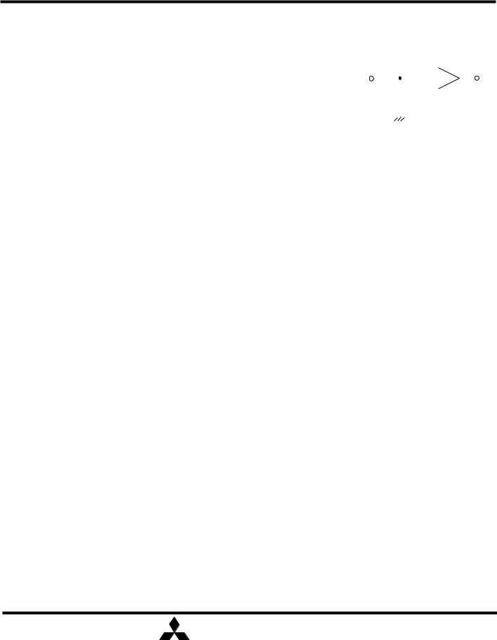
(1) TEST CONDITIONS
Supply voltage |
2.7V~3.6V |
|
|
|
|
|
1TTL |
|||
Input pulse |
VIH=2.4V,VIL=0.4V |
DQ |
|
|
|
|
||||
|
|
|
|
|
|
|
|
|||
Input rise time and fall time |
5ns |
|
|
|
|
|
|
|
|
|
|
|
|
|
CL |
|
|||||
|
|
|
|
|
|
|
|
|||
|
|
|
|
|
|
|
|
|||
|
VOH=VOL=1.5V |
|
|
|
|
|
|
|||
Reference level |
|
|
|
|
|
Including scope and |
||||
Transition is measured ±500mV from |
|
|
|
|
|
|||||
|
|
|
|
|
jig capacitance |
|||||
|
|
|
|
|
|
|||||
|
steady state voltage.(for ten,tdis) |
|
|
|
|
|
|
|
|
|
|
|
|
|
|||||||
Output loads |
Fig.1,CL=30pF |
|
Fig.1 Output load |
|||||||
CL=5pF (for ten,tdis) |
|
|
|
|
|
|
|
|
|
|
|
|
|
|
|
|
|
|
|
|
|
|
|
|
|
|
|
|
|
|
|
|
(2) READ CYCLE
|
|
|
|
|
|
|
|
|
|
|
|
Limits |
|
|
|
Symbol |
Parameter |
M5M5V408B |
|
M5M5V408B |
Units |
||||||||||
FP,TP,RT,KV,KR-85 |
|
FP,TP,RT,KV,KR-10 |
|||||||||||||
|
|
|
|
|
|
|
|
|
|
Min |
Max |
|
Min |
Max |
|
tCR |
Read cycle time |
85 |
|
|
100 |
|
ns |
||||||||
ta(A) |
Address access time |
|
85 |
|
|
100 |
ns |
||||||||
ta(S) |
Chip select access time |
|
85 |
|
|
100 |
ns |
||||||||
|
|
|
|
|
|
|
|
|
|
|
|
||||
ta(OE) |
Output enable access time |
|
45 |
|
|
50 |
ns |
||||||||
tdis(S) |
Output disable time after |
|
|
high |
|
30 |
|
|
35 |
ns |
|||||
S |
|
|
|
||||||||||||
tdis(OE) |
|
|
30 |
|
|
35 |
ns |
||||||||
Output disable time after |
OE |
high |
|
|
|
||||||||||
ten(S) |
Output enable time after |
|
|
|
|
|
low |
10 |
|
|
10 |
|
ns |
||
S |
|
|
|||||||||||||
ten(OE) |
Output enable time after |
|
|
|
|
|
low |
5 |
|
|
5 |
|
ns |
||
OE |
|
|
|||||||||||||
tV(A) |
Data valid time after address |
10 |
|
|
10 |
|
ns |
||||||||
(3) WRITE CYCLE
|
|
|
|
|
|
|
|
|
|
|
|
Limits |
|
|
|
Symbol |
Parameter |
M5M5V408B |
M5M5V408B |
Units |
|||||||||||
FP,TP,RT,KV,KR-85 |
FP,TP,RT,KV,KR-10 |
||||||||||||||
|
|
|
|
|
|
|
|
|
|
|
Min |
Max |
Min |
Max |
|
tCW |
Write cycle time |
85 |
|
100 |
|
ns |
|||||||||
|
|
|
|
|
|
|
|
|
|
|
|
|
|
|
|
tw(W) |
Write pulse width |
60 |
|
75 |
|
ns |
|||||||||
|
|
|
|
|
|
|
|
|
|
|
|
|
|
|
|
tsu(A) |
Address set up time |
0 |
|
0 |
|
ns |
|||||||||
tsu(A-WH) |
Address set up time with respect to |
|
high |
70 |
|
85 |
|
ns |
|||||||
W |
|
|
|||||||||||||
tsu(S) |
Chip select set up time |
70 |
|
85 |
|
ns |
|||||||||
tsu(D) |
Data set up time |
35 |
|
40 |
|
ns |
|||||||||
th(D) |
Data hold time |
0 |
|
0 |
|
ns |
|||||||||
trec(W) |
Write recovery time |
0 |
|
0 |
|
ns |
|||||||||
|
|
|
|
|
|
|
|
|
|
30 |
|
35 |
ns |
||
tdis(W) |
Output disable time after W low |
|
|
||||||||||||
tdis(OE) |
|
|
|
|
|
|
30 |
|
35 |
ns |
|||||
Output disable time after |
OE |
high |
|
|
|||||||||||
ten(W) |
Output enable time after |
|
|
high |
5 |
|
5 |
|
ns |
||||||
|
W |
|
|
||||||||||||
ten(OE) |
Output enable time after |
|
low |
5 |
|
5 |
|
ns |
|||||||
OE |
|
|
|||||||||||||
MITSUBISHI ELECTRIC |
5 |
 Loading...