


Mitsubishi M5M44265CJ-6, M5M44265CJ-5S, M5M44265CJ-5, M5M44265CTP-7S, M5M44265CTP-7 Datasheet
...MITSUBISHI LSIs MITSUBISHI LSIs
M5M44265CJ,TP-5,-6,-7,-5,-5S,-6,-6S,-7,-7S
-5S,-6S,-7S
EDOEDO(HYPER(HYPERPAGEPAGEMODE)MODE)41943044194304-BIT-BIT(262144(262144-WORD-WORDBYBY16-BIT)16-BIT)DYNAMICRAMRAM
DESCRIPTION
This is a family of 262144-word by 16-bit dynamic RAMs with Hyper Page mode fuction, fabricated with the high performance CMOS process, and is ideal for the buffer memory systems of personal computer graphics and HDD where high speed, low power dissipation, and low costs are essential.
The use of double-layer metalization process technology and a single-transistor dynamic storage stacked capacitor cell provide high circuit density at reduced costs. Multiplexed address inputs permit both a reduction in pins and an increase in system densities. Self or extended refresh current is low enough for battery back-up application.
This device has 2CAS and 1W terminals with a refresh cycle of 512 cycles every 8.2ms.
FEATURES
|
|
|
|
|
|
|
|
|
|
|
|
Power |
|
|
RAS |
CAS |
Address |
OE |
Cycle |
|
|||||||
Type name |
access |
access |
access |
access |
time |
dissipa- |
|
||||||
|
time |
time |
time |
time |
tion |
|
|||||||
|
(max.ns) |
(max.ns) |
(max.ns) |
(max.ns) |
(min.ns) |
(typ.mW) |
|
||||||
|
|
|
|
|
|
|
|
|
|
|
|
||
M5M44265CXX-5,-5S |
50 |
|
13 |
|
25 |
13 |
|
90 |
625 |
|
|||
|
|
|
|
|
|
|
|
|
|
|
|
|
|
M5M44265CXX-6,-6S |
60 |
|
15 |
|
30 |
15 |
|
110 |
550 |
|
|||
|
|
|
|
|
|
|
|
|
|
|
|
|
|
M5M44265CXX-7,-7S |
70 |
|
20 |
|
35 |
20 |
|
130 |
475 |
|
|||
XX=J,TP |
|
|
|
|
|
|
|
|
|
|
|
|
|
Standard 40pin SOJ, 44 pin TSOP (II) |
|
|
|
|
|
|
|||||||
Single 5V±10% supply |
|
|
|
|
|
|
|
|
|
|
|||
Low stand-by power dissipation |
|
|
|
|
|
|
|
||||||
CMOS Input level |
|
|
|
|
|
|
|
5.5mW (Max) |
|||||
CMOS Input level |
|
|
|
|
|
|
|
550µW (Max)* |
|||||
Operating power dissipation |
|
|
|
|
|
|
|
||||||
M5M44265Cxx-5,-5S |
|
|
|
|
|
|
|
688mW (Max) |
|||||
M5M44265Cxx-6,-6S |
|
|
|
|
|
|
|
605mW (Max) |
|||||
M5M44265Cxx-7,-7S |
|
|
|
|
|
|
|
523mW (Max) |
|||||
Self refresh capability* |
|
|
|
|
|
|
|
|
|
|
|||
Self refresh current |
|
|
|
|
|
|
|
150µA (Max) |
|||||
Extended refresh capability |
|
|
|
|
|
|
|
||||||
Extended refresh current |
|
|
|
|
150µA (Max) |
||||||||
 Hyper-page mode (512-column random access), Read-modify- write, RAS-only refresh, CAS before RAS refresh, Hidden refresh capabilities.
 Early-write mode, OE and W to control output buffer impedance
 512 refresh cycles every 8.2ms (A0~A8)
 512 refresh cycles every 128ms (A0~A8)*
 Byte or word control for Read/Write operation (2CAS, 1W type)
*: Applicable to self refresh version (M5M44265CJ,TP-5S,-6S,-7S
:option) only
APPLICATION
Microcomputer memory, Refresh memory for CRT, Frame Buffer memory for CRT
PIN DESCRIPTION
|
|
Pin name |
Function |
||||||
|
|
A0~A8 |
Address inputs |
||||||
DQ1~DQ16 |
Data inputs / outputs |
||||||||
|
|
|
|
|
|
|
|
Row address strobe input |
|
RAS |
|||||||||
|
|
|
|
|
|
|
|
Lower byte control |
|
LCAS |
|||||||||
column address strobe input |
|||||||||
|
|
|
|
|
|
|
|
||
|
|
|
|
|
|
|
|
Upper byte control |
|
UCAS |
|||||||||
column address strobe input |
|||||||||
|
|
|
|
|
|
|
|
||
|
|
|
|
|
|
|
|
Write control input |
|
|
W |
|
|
|
|||||
|
|
|
|
Output enable input |
|||||
OE |
|||||||||
VCC |
Power supply (+5V) |
||||||||
|
|
VSS |
Ground (0V) |
||||||
1
PIN CONFIGURATION (TOP VIEW)
(5V)VCC |
|
|
|
|
|
|
|
VSS(0V) |
||||||||||||
1 |
|
|
|
|
40 |
|
||||||||||||||
|
DQ1 |
|
|
|
|
|
|
|
DQ16 |
|||||||||||
|
2 |
|
|
|
|
39 |
|
|||||||||||||
|
DQ2 |
|
|
|
|
|
|
|
DQ15 |
|||||||||||
3 |
|
|
|
|
38 |
|||||||||||||||
|
DQ3 |
|
|
|
|
|
|
|
DQ14 |
|||||||||||
|
4 |
|
|
|
|
37 |
|
|||||||||||||
|
DQ4 |
|
|
|
|
|
|
|
DQ13 |
|||||||||||
|
5 |
|
|
|
|
36 |
|
|||||||||||||
(5V)VCC |
|
|
|
|
|
|
|
VSS(0V) |
||||||||||||
6 |
|
|
|
|
35 |
|
||||||||||||||
|
DQ5 |
|
|
|
|
|
|
|
DQ12 |
|||||||||||
|
7 |
|
|
|
|
34 |
|
|||||||||||||
|
DQ6 |
|
|
|
|
|
|
|
DQ11 |
|||||||||||
|
8 |
|
|
|
|
33 |
|
|||||||||||||
|
DQ7 |
|
|
|
|
|
|
|
DQ10 |
|||||||||||
|
9 |
|
|
|
|
32 |
|
|||||||||||||
|
DQ8 |
|
|
|
|
|
|
|
DQ9 |
|||||||||||
|
10 |
|
|
|
|
31 |
|
|||||||||||||
|
NC |
|
|
|
|
|
|
|
NC |
|||||||||||
11 |
|
|
|
|
30 |
|
||||||||||||||
|
NC |
|
|
|
|
|
|
|
|
|
|
|
|
|
|
|||||
|
12 |
|
|
|
|
29 |
|
LCAS |
||||||||||||
|
|
|
|
|
|
|
|
|
|
|
|
|
|
|
|
|
|
|
|
|
|
|
W |
13 |
|
|
|
|
28 |
|
UCAS |
||||||||||
|
|
|
|
|
|
|
|
|
|
|
|
|
|
|
|
|
|
|
|
|
|
RAS |
14 |
|
|
|
|
27 |
|
OE |
|||||||||||
|
|
|
|
|
|
|
|
|
|
|
|
|
|
|
|
|
|
|
|
|
|
NC |
15 |
|
|
|
|
26 |
|
A8 |
|||||||||||
|
|
A0 |
|
|
|
|
|
|
|
A7 |
||||||||||
|
|
16 |
|
|
|
|
25 |
|
||||||||||||
|
|
A1 |
|
|
|
|
|
|
|
A6 |
||||||||||
|
|
17 |
|
|
|
|
24 |
|
||||||||||||
|
|
A2 |
|
|
|
|
|
|
|
|
|
|
|
|
|
|
||||
|
|
18 |
|
|
|
|
23 |
|
A5 |
|||||||||||
|
|
A3 |
|
|
|
|
|
|
|
|
|
|
|
|
|
|
||||
|
|
19 |
|
|
|
|
22 |
|
A4 |
|||||||||||
|
|
|
|
|
|
|
|
|
|
|
|
|
|
VSS(0V) |
||||||
(5V)VCC |
20 |
|
|
|
|
21 |
|
|||||||||||||
|
|
|
|
|
|
|
|
|
|
|
|
|
|
|
|
|
|
|
|
|
|
Outline 40P0K (400mil SOJ) |
|||||||||||||||||||
(5V)VCC |
|
|
|
|
VSS(0V) |
|||||||||||||||
|
|
|
|
|
|
|
||||||||||||||
1 |
|
|
44 |
|
||||||||||||||||
|
DQ1 |
|
|
|
|
|
|
|
|
|
||||||||||
|
2 |
|
|
43 |
|
DQ16 |
||||||||||||||
|
DQ2 |
|
|
|
|
|
|
|
|
|
||||||||||
|
3 |
|
|
42 |
|
DQ15 |
||||||||||||||
|
|
|
|
|
|
|
|
|
|
DQ14 |
||||||||||
|
DQ3 |
4 |
|
|
41 |
|
||||||||||||||
|
DQ4 |
|
|
|
|
|
DQ13 |
|||||||||||||
|
5 |
|
|
40 |
|
|||||||||||||||
|
|
|
|
|
|
|
|
|||||||||||||
(5V)VCC |
6 |
|
|
|
|
39 |
|
VSS(0V) |
||||||||||||
|
DQ5 |
|
|
|
|
|
|
|
DQ12 |
|||||||||||
|
7 |
|
|
|
|
38 |
|
|||||||||||||
|
|
|
|
|
|
|
|
|
|
|
|
|
|
DQ11 |
||||||
|
DQ6 |
8 |
|
|
|
|
37 |
|
||||||||||||
|
DQ7 |
|
|
|
|
|
|
|
DQ10 |
|||||||||||
9 |
|
|
36 |
|
||||||||||||||||
|
DQ8 |
|
|
|
|
|
DQ9 |
|||||||||||||
|
10 |
|
|
35 |
|
|||||||||||||||
|
NC |
|
|
|
|
|
NC |
|||||||||||||
|
13 |
|
|
32 |
|
|||||||||||||||
|
NC |
|
|
|
|
|
|
|
|
|
||||||||||
|
14 |
|
|
|
|
31 |
|
LCAS |
||||||||||||
|
|
|
|
|
|
|
|
|
|
|
|
|
|
|
||||||
|
|
W |
15 |
|
|
|
|
30 |
|
UCAS |
||||||||||
|
|
|
|
|
|
|
|
|
|
|
|
|||||||||
|
RAS |
|
16 |
|
|
|
|
29 |
|
OE |
||||||||||
|
|
|
|
|
|
|
|
|
|
|
|
|
|
|
|
|
|
|
|
|
|
NC |
17 |
|
|
|
|
28 |
|
A8 |
|||||||||||
|
|
|
|
|
|
|
|
|
|
|
|
|
|
|
|
|
|
|
|
|
|
|
A0 |
18 |
|
|
|
|
27 |
|
A7 |
||||||||||
|
|
|
|
|
|
|
|
|
|
|
|
|
|
|
|
|
|
|
|
|
|
|
A1 |
19 |
|
|
|
|
26 |
|
A6 |
||||||||||
|
|
|
|
|
|
|
|
|
|
|
|
|
|
|
|
|
|
|
|
|
|
|
A2 |
20 |
|
|
|
|
25 |
|
A5 |
||||||||||
|
|
|
|
|
|
|
|
|
|
|
|
|
|
A4 |
||||||
|
|
A3 |
21 |
|
|
|
|
24 |
|
|||||||||||
|
|
|
|
|
|
|
|
|
|
|
|
|
|
|
|
|
|
|
|
|
(5V)VCC |
22 |
|
|
|
|
23 |
|
VSS(0V) |
||||||||||||
|
|
|
|
|
|
|
|
|
|
|
|
|
|
|
|
|
|
|
|
|
Outline 44P3W-R (400mil TSOP Nomal Bend)
NC: NO CONNECTION
MITSUBISHI LSIs
M5M44265CJ,TP-5,-6,-7,-5S,-6S,-7S
EDO (HYPER PAGE MODE) 4194304-BIT (262144-WORD BY 16-BIT) DYNAMIC RAM
FUNCTION
In addition to Hyper page mode, normal read, write and read- modify-write operations the M5M44265CJ, TP provides a number of
of other functions, e.g., RAS-only refresh and delayed-write. The input conditions for each are shown in Table 1.
Table 1 Input conditions for each mode
|
|
|
|
Operation |
|
|
|
|
|
|
Inputs |
|
|
|
|
|
|
|
Input/Output |
||||
|
|
|
|
|
|
|
RAS |
|
|
LCAS |
|
|
UCAS |
|
|
W |
|
|
OE |
|
DQ1~DQ8 |
|
DQ9~DQ16 |
|
Lower byte read |
ACT |
|
ACT |
|
NAC |
NAC |
ACT |
DOUT |
|
OPN |
||||||||||||
|
Upper byte read |
ACT |
|
NAC |
|
ACT |
NAC |
ACT |
OPN |
|
DOUT |
||||||||||||
|
Word read |
ACT |
|
ACT |
|
ACT |
NAC |
ACT |
DOUT |
|
DOUT |
||||||||||||
|
Lower byte write |
ACT |
|
ACT |
|
NAC |
ACT |
NAC |
DIN |
|
DNC |
||||||||||||
|
Upper byte write |
ACT |
|
NAC |
|
ACT |
ACT |
NAC |
DNC |
|
DIN |
||||||||||||
|
Word write |
ACT |
|
ACT |
|
ACT |
ACT |
NAC |
DIN |
|
DIN |
||||||||||||
|
|
|
only refresh |
|
|
|
|
NAC |
|
NAC |
DNC |
DNC |
|
|
OPN |
||||||||
|
RAS |
ACT |
OPN |
||||||||||||||||||||
|
Hidden refresh |
ACT |
|
ACT |
|
ACT |
NAC |
ACT |
DOUT |
|
DOUT |
||||||||||||
|
|
before |
|
(Extended*) refresh |
ACT |
|
ACT |
|
ACT |
DNC |
DNC |
OPN |
|
OPN |
|||||||||
|
CAS |
RAS |
|
|
|
||||||||||||||||||
|
Self refresh* |
ACT |
|
ACT |
|
ACT |
DNC |
DNC |
OPN |
|
OPN |
||||||||||||
|
Stand-by |
NAC |
|
DNC |
|
DNC |
DNC |
DNC |
OPN |
|
OPN |
||||||||||||
Note : ACT : active, NAC : nonactive, DNC : don' t care, OPN : open
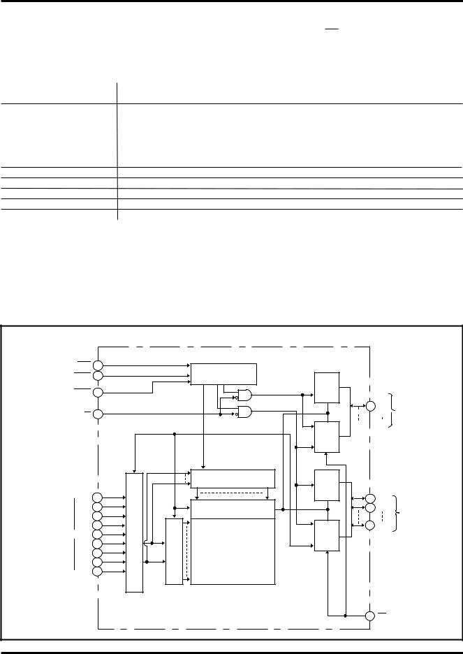
BLOCK DIAGRAM
ROW ADDRESS STROBE INPUT RAS
LOWER BYTE CONTROL COLUMN ADDRESS LCAS
STROBE INPUT
UPPER BYTE CONTROL UCAS COLUMN ADDRESS
STROBE INPUT
WRITE CONTROL
INPUT W
 A0
A0
A1
A2
A3 ADDRESS INPUTS  A4
A4
A5
A6
A7
 A8
A8
|
|
|
CLOCK GENERATOR |
|
|
|
|
CIRCUIT |
(8)LOWER |
|
|
|
|
|
|
|
|
LOWER |
DATA IN |
|
|
|
BUFFER |
|
|
|
|
|
|
|
|
|
UPPER |
|
|
|
|
|
(8)LOWER |
|
|
|
|
DATA OUT |
|
|
|
|
BUFFER |
|
A0~A8 |
|
|
|
|
|
|
COLUMN DECODER |
(8) UPPER |
|
|
|
|
DATA IN |
|
|
|
|
BUFFER |
|
|
|
SENSE REFRESH |
|
ROW |
|
|
AMPLIFIER & I /O CONTROL |
|
|
|
|
|
|
& |
|
|
|
|
COLU- |
|
|
|
(8)UPPER |
MN |
|
|
|
|
|
|
|
DATA OUT |
|
ADD- |
|
|
|
|
|
|
MEMORY CELL |
BUFFER |
|
RESS |
|
ROW |
||
A0~ |
|
|||
BUFF- |
DECO |
(4194304 BITS) |
|
|
ER |
|
|||
A8 |
DER |
|
|
|
|
|
|
|
|

 VCC (5V)

 VSS (0V)

 DQ1
DQ1
DQ2 LOWER DATA


 INPUTS / OUTPUTS
 DQ8
DQ8

 VCC (5V)

 VSS (0V)
DQ9 |
|
DQ10 |
UPPER DATA |
|
INPUTS / OUTPUTS |
DQ16 |
|

 VCC (5V)

 VSS (0V)
OUTPUT ENABLE
OE INPUT
2

MITSUBISHI LSIs
M5M44265CJ,TP-5,-6,-7,-5S,-6S,-7S
EDO (HYPER PAGE MODE) 4194304-BIT (262144-WORD BY 16-BIT) DYNAMIC RAM
ABSOLUTE MAXIMUM RATINGS
Symbol |
|
|
|
|
|
|
Parameter |
|
|
|
|
|
|
|
|
|
|
|
|
|
|
|
|
|
|
|
|
|
|
Conditions |
|
|
|
|
|
Ratings |
|
Unit |
|||||||||
VCC |
Supply voltage |
|
|
|
|
|
|
|
|
|
|
|
|
|
|
|
|
|
|
|
|
|
|
|
|
|
|
|
|
|
|
|
|
|
|
|
-1~7 |
|
|
V |
|||||||
V I |
Input voltage |
|
|
|
|
With respect to VSS |
|
|
|
|
|
-1~7 |
|
|
V |
||||||||||||||||||||||||||||||||
VO |
Output voltage |
|
|
|
|
|
|
|
|
|
|
|
|
|
|
|
|
|
|
|
|
|
|
|
|
|
|
|
|
|
|
|
|
|
|
|
-1~7 |
|
|
V |
|||||||
I O |
Output current |
|
|
|
|
|
|
|
|
|
|
|
|
|
|
|
|
|
|
|
|
|
|
|
|
|
|
|
|
|
|
|
|
|
|
|
50 |
|
|
mA |
|||||||
Pd |
Power dissipation |
|
Ta=25 C |
|
|
|
|
|
|
|
|
|
|
1000 |
|
|
mW |
||||||||||||||||||||||||||||||
Topr |
Operating temperature |
|
|
|
|
|
|
|
|
|
|
|
|
|
|
|
|
|
|
|
|
|
|
|
|
|
|
|
|
|
|
|
|
|
|
|
0~70 |
|
|
˚C |
|||||||
Tstg |
Storage temperature |
|
|
|
|
|
|
|
|
|
|
|
|
|
|
|
|
|
|
|
|
|
|
|
|
|
|
|
|
|
|
|
|
|
|
|
-65~150 |
|
˚C |
||||||||
RECOMMENDED OPERATING CONDITIONS (Ta=0~70˚C, unless otherwise noted) (Note 1) |
|
|
|
|
|||||||||||||||||||||||||||||||||||||||||||
|
|
|
|
|
|
|
|
|
|
|
|
|
|
|
|
|
|
|
|
|
|
|
|
|
|
|
|
|
|
|
|
|
|
|
|
|
|
|
|
|
|
|
|
|
|
|
|
Symbol |
|
|
|
|
|
|
Parameter |
|
|
|
|
|
|
|
|
|
|
|
|
|
Limits |
|
|
|
|
|
Unit |
|
|
|
|
|
|
||||||||||||||
|
|
|
|
|
|
|
|
|
Min |
|
Nom |
|
|
Max |
|
|
|
|
|
|
|
||||||||||||||||||||||||||
|
|
|
|
|
|
|
|
|
|
|
|
|
|
|
|
|
|
|
|
|
|
|
|
|
|
||||||||||||||||||||||
VCC |
Supply voltage |
|
4.5 |
|
|
|
|
|
|
|
|
5.0 |
|
|
|
5.5 |
|
|
V |
|
|
|
|
|
|
||||||||||||||||||||||
VSS |
Supply voltage |
|
0 |
|
|
|
|
|
|
|
|
0 |
|
|
|
0 |
|
|
V |
|
|
|
|
|
|
||||||||||||||||||||||
VIH |
|
High-level input voltage, all inputs |
2.4 |
|
|
|
|
|
|
|
|
|
|
|
|
|
|
|
|
|
|
6.0 |
|
|
V |
|
|
|
|
|
|
||||||||||||||||
VIL |
|
Low-level input voltage, all inputs |
-0.5** |
|
|
|
|
|
|
|
|
|
|
|
|
|
|
0.8 |
|
|
V |
|
|
|
|
|
|
||||||||||||||||||||
Note 1 : All voltage values are with respect to |
VSS. |
|
|
|
|
|
|
|
|
|
|
|
|
|
|
|
|
|
|
|
|
|
|
|
|
|
|
|
|
|
|
|
|
|
|
|
|
|
|
||||||||
* * : VIL(min) is -2.0V when pulse width is less than 25ns. (Pulse width is with respect to Vss.) |
|
|
|
|
|
|
|
|
|
||||||||||||||||||||||||||||||||||||||
ELECTRICAL CHARACTERISTICS (Ta=0~70˚C, VCC=5V±10%, VSS=0V, unless otherwise noted) (Note 2) |
|
|
|||||||||||||||||||||||||||||||||||||||||||||
|
|
|
|
|
|
|
|
|
|
|
|
|
|
|
|
|
|
|
|
|
|
|
|
|
|
|
|
|
|
|
|
|
|
|
|
|
|
|
|
|
|
|
|
|
|
|
|
Symbol |
|
|
|
|
|
|
|
Parameter |
|
|
|
|
|
|
|
|
|
|
|
|
|
|
|
|
|
Test |
conditions |
|
|
|
|
|
Limits |
|
Unit |
||||||||||||
|
|
|
|
|
|
|
|
|
|
|
|
|
|
|
|
|
|
|
|
|
|
|
|
|
|
|
|
Min |
Typ |
|
Max |
||||||||||||||||
|
|
|
|
|
|
|
|
|
|
|
|
|
|
|
|
|
|
|
|
|
|
|
|
|
|
|
|
|
|
|
|
|
|
|
|
|
|
|
|
|
|
|
|
|
|||
VOH |
High-level output voltage |
|
IOH=-2mA |
|
|
|
|
|
|
|
|
|
2.4 |
|
|
VCC |
V |
||||||||||||||||||||||||||||||
VOL |
Low-level output voltage |
|
IOL=2mA |
|
|
|
|
|
|
|
|
|
|
|
|
|
|
|
|
|
|
|
0 |
|
|
0.4 |
V |
||||||||||||||||||||
IOZ |
Off-state output current |
|
Q floating 0V £ VOUT £ 5.5V |
|
|
|
-10 |
|
|
10 |
µA |
||||||||||||||||||||||||||||||||||||
I I |
|
Input current |
|
|
|
|
0V £ VIN £ +6.0V, Other inputs pins=0V |
-10 |
|
|
10 |
µA |
|||||||||||||||||||||||||||||||||||
|
|
Average supply current |
M5M44265C-5,-5S |
|
|
|
|
|
|
|
|
|
|
|
|
|
|
|
|
|
|
|
|
|
|
|
|
|
|
|
|
|
|
|
|
|
|
|
|
125 |
|
||||||
ICC1(AV) |
|
|
|
RAS, CAS cycling |
|
|
|
|
|
|
|
|
|||||||||||||||||||||||||||||||||||
|
|
|
|
|
|
|
|
|
|
|
|
|
|||||||||||||||||||||||||||||||||||
|
|
|
|
|
|
|
|
|
|
||||||||||||||||||||||||||||||||||||||
|
from Vcc, operating |
M5M44265C-6,-6S |
|
|
tRC=tWC=min. |
|
|
|
|
|
|
|
|
|
|
|
|
110 |
mA |
||||||||||||||||||||||||||||
|
|
|
|
|
(Note 3,4,5) |
|
|
|
output open |
|
|
|
|
|
|
|
|
|
|
|
|
|
|
||||||||||||||||||||||||
|
|
|
|
|
M5M44265C-7,-7S |
|
|
|
|
|
|
|
|
|
|
|
|
95 |
|
||||||||||||||||||||||||||||
|
|
|
|
|
|
|
|
|
|
|
|
|
|
|
|
|
|
|
|
|
|
|
|
|
|
|
|
|
|
|
|
|
|
|
|
|
|
|
|
|
|
||||||
|
|
|
|
|
|
|
|
|
|
|
|
|
|
|
|
|
|
|
|
|
|
|
|
|
|
|
|
|
|
|
|
|
|
|
|
|
|
|
|
|
|
|
|
||||
|
|
|
|
|
|
|
|
|
|
|
|
|
|
|
|
|
|
|
|
|
|
|
|
|
|
|
|
|
|
|
|
|
|
|
|
|
|
|
|
2 |
|
||||||
|
|
|
|
|
|
|
|
|
|
|
RAS= CAS =VIH, output open |
|
|
|
|
|
|
|
|||||||||||||||||||||||||||||
ICC2 |
Supply current from VCC, stand-by (Note 6) |
|
|
|
|
|
|
|
|
|
|
|
|
³ VCC -0.5V |
|
|
|
|
|
|
|
1.0 |
mA |
||||||||||||||||||||||||
|
RAS= |
CAS |
|
|
|
|
|
|
|
||||||||||||||||||||||||||||||||||||||
|
|
|
|
|
|
|
|
|
|
|
output open |
|
|
|
|
|
|
|
|
|
|
|
|
0.1* |
|
||||||||||||||||||||||
|
|
Average supply current |
M5M44265C-5,-5S |
|
|
|
|
|
|
|
|
|
|
|
|
|
|
|
|
|
|
|
|
|
|
|
|
|
|
|
|
|
|
|
|
|
|
|
|
125 |
|
||||||
|
|
|
|
RAS cycling, CAS=VIH |
|
|
|
|
|
|
|
|
|||||||||||||||||||||||||||||||||||
|
|
|
|
|
|
|
|
|
|
|
|
|
|
|
|
|
|
|
|
|
|||||||||||||||||||||||||||
ICC3(AV) |
|
from Vcc, RAS only |
M5M44265C-6,-6S |
|
|
|
|
|
|
|
|
|
110 |
|
|||||||||||||||||||||||||||||||||
|
|
|
tRC=min. |
|
|
|
|
|
|
|
|
|
|
|
|
|
|
|
|
|
|
|
|
|
|
mA |
|||||||||||||||||||||
|
|
refresh mode |
|
|
|
output open |
|
|
|
|
|
|
|
|
|
|
|
|
|
|
|||||||||||||||||||||||||||
|
M5M44265C-7,-7S |
|
|
|
|
|
|
|
|
|
|
|
|
95 |
|
||||||||||||||||||||||||||||||||
|
|
|
|
|
|
(Note 3,5) |
|
|
|
|
|
|
|
|
|
|
|
|
|
|
|
|
|
|
|
|
|
|
|
|
|
|
|
|
|
|
|
|
|
|
|
|
|
||||
|
|
Average supply current |
M5M44265C-5,-5S |
|
|
|
|
|
|
|
|
|
|
|
|
|
|
|
|
|
|
|
|
|
|
|
|
|
|
|
|
|
|
|
|
|
|
|
|
125 |
|
||||||
|
|
|
|
RAS=VIL, CAS cycling |
|
|
|
|
|
|
|
|
|||||||||||||||||||||||||||||||||||
|
|
from Vcc |
|
|
|
|
|
|
|
|
|
|
|
|
|
|
|
||||||||||||||||||||||||||||||
|
|
|
|
|
M5M44265C-6,-6S |
|
|
|
|
|
|
|
|
|
|||||||||||||||||||||||||||||||||
ICC4(AV) |
|
|
|
|
|
|
tPC=min. |
|
|
|
|
|
|
|
|
|
|
|
|
|
|
|
|
|
|
|
|
|
|
110 |
mA |
||||||||||||||||
|
Hyper page mode |
|
|
|
|
|
|
|
|
|
|
|
|
|
|
|
|
|
|
|
|
|
|
|
|
||||||||||||||||||||||
|
|
|
|
|
output open |
|
|
|
|
|
|
|
|
|
|
|
|
|
|
||||||||||||||||||||||||||||
|
|
|
|
|
|
(Note 3,4,5) |
M5M44265C-7,-7S |
|
|
|
|
|
|
|
|
|
|
|
|
|
|
95 |
|
||||||||||||||||||||||||
|
|
|
|
|
|
|
|
|
|
|
|
|
|
|
|
|
|
|
|
|
|
|
|
|
|
|
|
|
|
|
|
|
|
|
|
|
|
|
|
|
|
|
|||||
|
|
|
|
|
|
|
|
|
|
|
|
|
|
|
|
|
|
|
|
|
|
|
|
|
|
|
|
|
|
|
|
|
|
|
|
|
|
|
|
|
|
|
|
|
|
|
|
|
Average supply current |
M5M44265C-5,-5S |
|
|
|
|
|
|
|
|
|
|
|
|
|
|
|
|
|
|
|
|
|
|
|
|
|
|
|
|
|
|
|
|
|
|
|
|
115 |
|
|||||||
|
|
|
CAS before RAS refresh cycling |
|
|
|
|
||||||||||||||||||||||||||||||||||||||||
|
from Vcc |
|
|
|
|
|
|
|
|
|
|
|
|||||||||||||||||||||||||||||||||||
|
|
|
|
|
|
|
|
|
|
||||||||||||||||||||||||||||||||||||||
ICC6(AV) |
|
|
before |
|
|
refresh |
M5M44265C-6,-6S |
|
|
tRC=min. |
|
|
|
|
|
|
|
|
|
|
|
|
|
|
|
|
|
|
|
|
|
|
100 |
mA |
|||||||||||||
CAS |
RAS |
|
|
|
|
|
|
|
|
|
|
|
|
|
|
|
|
|
|
|
|
|
|
||||||||||||||||||||||||
|
mode |
(Note 3,5) |
M5M44265C-7,-7S |
|
|
output open |
|
|
|
|
|
|
|
|
|
|
|
|
85 |
|
|||||||||||||||||||||||||||
|
|
|
|
|
|
|
|
|
|
|
|
|
|
|
|
|
|
|
|
|
|
|
|
|
|
|
|
|
|
|
|
|
|
|
|
|
|
||||||||||
|
|
|
|
|
|
|
|
|
|
|
|
|
|
|
|
|
|
|
|
|
|
|
|
|
|
|
|
|
|
|
|
|
|
|
|
|
|
|
|
|
|
||||||
|
|
|
|
|
|
|
|
|
|
|
|
|
|
|
|
|
cycling |
|
£ 0.2V or |
|
|
|
|
|
|
|
|||||||||||||||||||||
|
|
|
|
|
|
|
|
|
|
|
|
|
RAS |
CAS |
CAS |
|
|
|
|
|
|||||||||||||||||||||||||||
|
|
|
|
|
|
|
|
|
|
|
|
before |
RAS |
refresh cycling |
|
|
|
|
|
|
|
|
|
||||||||||||||||||||||||
|
|
|
|
|
|
|
|
|
|
|
|
|
RAS |
£ 0.2V or ³ VCC-0.2V |
|
|
|
|
|
|
|
|
|
||||||||||||||||||||||||
|
|
Average supply current |
|
|
|
|
|
|
£ 0.2V or ³ VCC-0.2V |
|
|
|
|
|
|
|
|
|
|||||||||||||||||||||||||||||
|
|
|
|
|
CAS |
|
|
|
|
|
|
|
|
|
|||||||||||||||||||||||||||||||||
ICC8(AV)* |
|
from VCC |
|
|
|
|
|
|
|
£ 0.2V or ³ VCC-0.2V |
|
|
|
|
|
|
|
|
µA |
||||||||||||||||||||||||||||
|
|
|
|
|
|
|
W |
|
|
|
|
|
|
|
150 |
||||||||||||||||||||||||||||||||
|
|
Extended-refresh mode |
(Note 6) |
|
|
OE |
£ 0.2V or ³ VCC-0.2V |
|
|
|
|
|
|
|
|
|
|||||||||||||||||||||||||||||||
|
|
|
|
|
|
|
|
|
|
|
|
A0~A8 £ 0.2V or ³ VCC-0.2V |
|
|
|
|
|
|
|
|
|||||||||||||||||||||||||||
|
|
|
|
|
|
|
|
|
|
|
|
DQ=open |
|
|
|
|
|
|
|
|
|
|
|
|
|
|
|||||||||||||||||||||
|
|
|
|
|
|
|
|
|
|
|
|
tRC=250µs, tRAS=tRAS min~1µs |
|
|
|
|
|
|
|
|
|||||||||||||||||||||||||||
|
|
Average supply current from VCC |
|
|
|
|
|
|
|
|
|
|
|
|
|
|
|
|
|
|
|
|
|
|
|
|
|
|
|
|
|
|
|
|
|
|
|
|
|
||||||||
ICC9(AV)* |
|
RAS=CAS £ 0.2V |
|
|
|
|
|
|
|
150 |
µA |
||||||||||||||||||||||||||||||||||||
|
Self-refresh mode |
(Note 6) |
output open |
|
|
|
|
|
|
|
|
|
|
|
|
||||||||||||||||||||||||||||||||
|
|
|
|
|
|
|
|
|
|
|
|
|
|
|
|
||||||||||||||||||||||||||||||||
|
|
|
|
|
|
|
|
|
|
|
|
|
|
|
|
|
|
|
|
|
|
|
|
|
|
|
|
|
|
|
|
|
|
|
|
|
|
|
|
|
|
|
|
|
|
|
|
Note 2: Current flowing into an IC is positive, out is negative.
3:ICC1 (AV), ICC3 (AV), ICC4 (AV), and ICC6 (AV) are dependent on cycle rate. Maximum current is measured at the fastest cycle rate.
4:ICC1 (AV) and ICC4 (AV) are dependent on output loading. Specified values are obtained with the output open.
3 |
5: Column Address can be changed once or less while |
|
|
|
|
RAS=VIL and CAS=VIH. |
|||||

MITSUBISHI LSIs
M5M44265CJ,TP-5,-6,-7,-5S,-6S,-7S
EDO (HYPER PAGE MODE) 4194304-BIT (262144-WORD BY 16-BIT) DYNAMIC RAM
CAPACITANCE (Ta=0~70˚C, VCC=5V±10%, VSS=0V, unless otherwise noted)
Symbol |
Parameter |
Test |
conditions |
|
|
|
Limits |
|
|
|
Unit |
||||||||||||||||||||||
|
|
Min |
Typ |
|
Max |
|
|||||||||||||||||||||||||||
|
|
|
|
|
|
|
|
|
|
|
|
|
|
|
|
|
|
|
|
|
|
|
|
|
|
|
|
|
|||||
CI (A) |
Input capacitance, address inputs |
VI=VSS |
|
|
|
|
|
|
|
|
5 |
|
|
pF |
|||||||||||||||||||
CI (CLK) |
Input capacitance, clock inputs |
f=1MHz |
|
|
|
|
|
|
|
|
7 |
|
|
pF |
|||||||||||||||||||
CI / O |
Input/Output capacitance, data ports |
VI=25mVrms |
|
|
|
|
|
|
|
|
7 |
|
|
pF |
|||||||||||||||||||
SWITCHING CHARACTERISTICS (Ta=0~70˚C, VCC=5V±10%, VSS=0V, unless otherwise noted, see notes 6,14,15) |
|
|
|
|
|||||||||||||||||||||||||||||
|
|
|
|
|
|
|
|
|
|
|
|
|
|
|
|
|
|
|
|
|
|
|
|
|
|
|
|
|
|
|
|
|
|
|
|
|
|
|
|
|
|
|
|
|
|
|
|
|
|
|
|
|
|
|
|
|
|
|
Limits |
|
|
|
|
|
|
|
|
Symbol |
|
|
|
|
|
|
|
|
Parameter |
|
M5M44265C-5,-5S |
M5M44265C-6,-6S |
M5M44265C-7,-7S |
|
Unit |
||||||||||||||||||
|
|
|
|
|
|
|
|
|
|
|
|
|
|
|
|
|
|
|
|
|
|||||||||||||
|
|
|
|
|
|
|
|
|
|
|
|
|
|
|
|
|
|
|
|
|
Min |
Max |
Min |
Max |
Min |
|
Max |
|
|
||||
tCAC |
|
|
|
|
|
|
|
|
|
|
|
|
|
|
|
|
|
(Note 7,8) |
|
|
13 |
|
|
15 |
|
|
|
20 |
|
|
ns |
||
Access time from |
CAS |
|
|
|
|
|
|
|
|
|
|
|
|
|
|
|
|
|
|
|
|
||||||||||||
tRAC |
|
|
|
|
|
|
|
|
|
|
|
|
|
|
|
(Note 7,9) |
|
|
|
|
|
|
|
|
|
|
|
|
ns |
||||
Access time from |
RAS |
|
|
|
|
|
|
|
|
|
|
|
|
|
|
50 |
|
|
60 |
|
|
|
70 |
|
|||||||||
tAA |
Columu address access time |
(Note 7,10) |
|
|
25 |
|
|
30 |
|
|
|
35 |
|
|
ns |
||||||||||||||||||
tCPA |
Access time from |
|
|
|
|
precharge |
(Note 7,11) |
|
|
28 |
|
|
33 |
|
|
|
38 |
|
|
ns |
|||||||||||||
CAS |
|
|
|
|
|
|
|
||||||||||||||||||||||||||
tOEA |
|
|
|
|
|
|
|
(Note 7) |
|
|
13 |
|
|
15 |
|
|
|
20 |
|
|
ns |
||||||||||||
Access time from |
OE |
|
|
|
|
|
|
|
|
|
|
|
|
|
|
||||||||||||||||||
tOHC |
Output hold time from |
|
|
|
|
|
(Note 13) |
|
5 |
|
5 |
|
5 |
|
|
|
|
|
|||||||||||||||
CAS |
|
|
|
|
|
|
|
ns |
|||||||||||||||||||||||||
tOHR |
Output hold time from |
|
|
|
|
|
(Note 13) |
|
5 |
|
5 |
|
5 |
|
|
|
|
|
|||||||||||||||
RAS |
|
|
|
|
|
|
|
ns |
|||||||||||||||||||||||||
tCLZ |
Output low impedance time from |
|
low |
(Note 7) |
|
5 |
|
5 |
|
5 |
|
|
|
|
|
||||||||||||||||||
CAS |
|
|
|
|
|
|
|
ns |
|||||||||||||||||||||||||
tOEZ |
Output disable time after |
|
|
|
|
|
high |
(Note 12) |
|
|
13 |
|
|
15 |
|
|
|
20 |
|
|
ns |
||||||||||||
OE |
|
|
|
|
|
|
|
|
|||||||||||||||||||||||||
tWEZ |
|
(Note 12) |
|
|
|
|
|
|
|
|
|
|
|
|
ns |
||||||||||||||||||
Output disable time after |
WE |
high |
|
|
13 |
|
|
15 |
|
|
|
20 |
|
||||||||||||||||||||
tOFF |
Output disable time after |
|
|
|
|
|
|
high |
(Note 12,13) |
|
|
13 |
|
|
15 |
|
|
|
20 |
|
|
ns |
|||||||||||
CAS |
|
|
|
|
|
|
|
||||||||||||||||||||||||||
tREZ |
Output disable time after |
|
|
high |
(Note 12,13) |
|
|
13 |
|
|
15 |
|
|
|
20 |
|
|
ns |
|||||||||||||||
RAS |
|
|
|
|
|
|
|
||||||||||||||||||||||||||
|
|
|
|
|
|
|
|
|
|
|
|
|
|
|
|
|
|
|
|
|
|
|
|
|
|
|
|
|
|
|
|
|
|
Note 6: An initial pause of 500µs is required after power-up followed by a minimum of eight initialization cycles (RAS-only refresh or CAS before RAS refresh cycles).
Note the RAS may be cycled during the initial pause. And 8 initialization cycles are required after prolonged periods (greater than 8.2ms) of RAS inactivity before proper device operation is achieved.
7:Measured with a load circuit equivalent to 1TTL and 50pF.
The reference levels for measuring of output signals are 2.0V(VOH) and 0.8V(VOL).
8:Assumes that tRCD ³ tRCD(max) and tASC ³ tASC(max) and tCP ³ tCP(max).
9:Assumes that tRCD £ tRCD(max) and tRAD £ tRAD(max). If tRCD or tRAD is greater than the maximum recommended value shown in this table, tRAC will increase by amount that tRCD exceeds the value shown.
10:Assumes that tRAD ³ tRAD(max) and tASC £ tASC(max).
11:Assumes that tCP £ tCP(max) and tASC ³ tASC(max).
12: tOEZ (max), tWEZ(max), tOFF(max) and tREZ(max) defines the time at which the output achieves the high impedance state (IOUT £ ±10µA ) and is not reference to VOH(min) or VOL(max).
13: Output is disabled after both RAS and CAS go to high.
4

MITSUBISHI LSIs
M5M44265CJ,TP-5,-6,-7,-5S,-6S,-7S
EDO (HYPER PAGE MODE) 4194304-BIT (262144-WORD BY 16-BIT) DYNAMIC RAM
TIMING REQUIREMENTS (For Read, Write, Read-Modify-Write, Refresh and Hyper-Page Mode Cycles)
(Ta=0~70˚C, VCC=5V±10%, VSS=0V, unless otherwise noted, see notes 14,15)
|
|
|
|
|
|
|
|
|
|
|
|
|
|
|
|
|
|
|
|
|
|
|
|
|
|
|
|
|
|
|
|
|
|
|
|
Limits |
|
|
|
|
Symbol |
|
|
|
|
|
|
|
|
|
|
|
|
|
|
|
|
|
|
Parameter |
|
M5M44265C-5,-5S |
M5M44265C-6,-6S |
M5M44265C-7,-7S |
Unit |
||||||||||||||||
|
|
|
|
|
|
|
|
|
|
|
|
|
|
|
|
|
|
|
|
|
|
|
|
|
|
|
|
|
|
|
|
|
|
Min |
Max |
Min |
Max |
Min |
Max |
|
tREF |
Refresh cycle time |
|
|
8.2 |
|
8.2 |
|
8.2 |
ms |
|||||||||||||||||||||||||||||||
tREF |
Refresh cycle time* |
|
|
128 |
|
128 |
|
128 |
ms |
|||||||||||||||||||||||||||||||
tRP |
|
|
high pulse width |
|
30 |
|
40 |
|
50 |
|
ns |
|||||||||||||||||||||||||||||
RAS |
|
|
|
|
||||||||||||||||||||||||||||||||||||
tRCD |
Delay time, |
|
|
|
|
|
|
|
|
low to |
|
|
|
|
low |
(Note 16) |
18 |
32 |
20 |
38 |
20 |
42 |
|
|||||||||||||||||
RAS |
CAS |
ns |
||||||||||||||||||||||||||||||||||||||
|
|
|
|
|
|
|
|
|
|
|
|
|
|
|
|
|
|
|
|
|
|
|
|
|
|
|
|
5 |
|
|
|
|
|
|
||||||
tCRP |
Delay time, |
CAS |
|
high to |
RAS |
|
|
low |
|
|
5 |
|
5 |
|
ns |
|||||||||||||||||||||||||
tRPC |
Delay time, |
|
|
|
high to |
|
|
low |
|
0 |
|
0 |
|
0 |
|
ns |
||||||||||||||||||||||||
RAS |
CAS |
|
|
|
|
|||||||||||||||||||||||||||||||||||
tCPN |
|
|
high pulse width |
|
8 |
|
10 |
|
|
|
ns |
|||||||||||||||||||||||||||||
CAS |
|
|
|
13 |
|
|||||||||||||||||||||||||||||||||||
|
Column address delay time from |
|
|
|
|
low |
|
13 |
25 |
15 |
30 |
|
35 |
ns |
||||||||||||||||||||||||||
tRAD |
RAS |
(Note 17) |
15 |
|||||||||||||||||||||||||||||||||||||
tASR |
Row address setup time before |
|
|
|
|
|
low |
|
0 |
|
0 |
|
0 |
|
ns |
|||||||||||||||||||||||||
RAS |
|
|
|
|
||||||||||||||||||||||||||||||||||||
tASC |
Column address setup time before |
|
|
low |
(Note 18) |
0 |
10 |
|
13 |
0 |
|
ns |
||||||||||||||||||||||||||||
CAS |
0 |
13 |
||||||||||||||||||||||||||||||||||||||
tRAH |
Row address hold time after |
|
|
low |
|
8 |
|
10 |
|
10 |
|
ns |
||||||||||||||||||||||||||||
RAS |
|
|
|
|
||||||||||||||||||||||||||||||||||||
tCAH |
Column address hold time after |
|
low |
|
8 |
|
10 |
|
10 |
|
ns |
|||||||||||||||||||||||||||||
CAS |
|
|
|
|
||||||||||||||||||||||||||||||||||||
tDZC |
Delay time, data to |
|
|
|
low |
(Note 19) |
0 |
|
|
|
|
|
|
|||||||||||||||||||||||||||
CAS |
|
0 |
|
0 |
|
ns |
||||||||||||||||||||||||||||||||||
tDZO |
|
|
|
|
(Note 19) |
0 |
|
|
|
|
|
|
||||||||||||||||||||||||||||
Delay time, data to |
OE |
low |
|
0 |
|
0 |
|
ns |
||||||||||||||||||||||||||||||||
tRDD |
|
Delay time, |
|
high to data |
(Note 20) |
13 |
|
15 |
|
20 |
|
|
||||||||||||||||||||||||||||
|
RAS |
|
|
|
ns |
|||||||||||||||||||||||||||||||||||
tCDD |
|
Delay time, |
|
|
high to data |
(Note 20) |
13 |
|
15 |
|
20 |
|
|
|||||||||||||||||||||||||||
|
CAS |
|
|
|
ns |
|||||||||||||||||||||||||||||||||||
tODD |
Delay time, |
|
high to data |
(Note 20) |
13 |
|
|
|
|
|
|
|||||||||||||||||||||||||||||
OE |
|
15 |
|
20 |
|
ns |
||||||||||||||||||||||||||||||||||
tT |
Transition time |
(Note 21) |
1 |
50 |
1 |
50 |
1 |
50 |
ns |
|||||||||||||||||||||||||||||||
Note 14: The timing requirements are assumed tT=2ns.
15:VIH(min) and VIL(max) are reference levels for measuring timing of input signals.
16:tRCD(max) is specified as a reference point only. If tRCD is less than tRCD(max), access time is tRAC. If tRCD is greater than tRCD(max), access time is controlled exclusively by tCAC or tAA.
17:tRAD(max) is specified as a reference point only. If tRAD ³ tRAD(max) and tASC £ tASC(max), access time is controlled exclusively by tAA.
18:tASC(max) is specified as a reference point only. If tRCD ³ tRCD(max) and tASC ³ tASC(max), access time is controlled exclusively by tCAC.
19:Either tDZC or tDZO must be satisfied.
20:Either tRDD or tCDD or tODD must be satisfied.
21:tT is measured between VIH(min) and VIL(max).
Read and Refresh Cycles
|
|
|
|
|
|
|
|
|
|
|
|
|
|
|
|
|
|
|
|
|
|
|
|
|
|
Limits |
|
|
|
|
Symbol |
|
|
|
|
|
|
|
|
|
|
|
|
|
|
|
|
|
|
Parameter |
|
M5M44265C-5,-5S |
M5M44265C-6,-6S |
M5M44265C-7,-7S |
Unit |
||||||
|
|
|
|
|
|
|
|
|
|
|
|
|
|
|
|
|
|
|
|
|
|
|
|
Min |
Max |
Min |
Max |
Min |
Max |
|
tRC |
|
Read cycle time |
|
90 |
|
110 |
|
130 |
|
ns |
||||||||||||||||||||
tRAS |
|
|
|
low pulse width |
|
|
10000 |
60 |
10000 |
70 |
10000 |
ns |
||||||||||||||||||
|
RAS |
|
50 |
|||||||||||||||||||||||||||
tCAS |
|
|
|
|
|
|
|
|
|
low pulse width |
|
8 |
|
10 |
|
13 |
|
ns |
||||||||||||
|
CAS |
|
10000 |
10000 |
10000 |
|||||||||||||||||||||||||
tCSH |
|
|
|
|
|
|
|
hold time after |
|
|
|
|
|
|
|
|
|
|
|
40 |
|
48 |
|
55 |
|
ns |
||||
|
CAS |
RAS low |
|
|
|
|
||||||||||||||||||||||||
|
|
|
|
|
|
|
|
|
|
|
|
|
|
|
|
|
|
|
||||||||||||
tRSH |
|
|
|
RAS |
|
|
hold time after |
CAS |
|
low |
|
13 |
|
15 |
|
20 |
|
ns |
||||||||||||
tRCS |
|
Read setup time before |
|
|
|
|
low |
|
|
|
0 |
|
0 |
|
ns |
|||||||||||||||
|
CAS |
|
0 |
|
|
|
||||||||||||||||||||||||
|
|
|
|
|
|
|
|
|
|
(Note 22) |
|
|
0 |
|
0 |
|
ns |
|||||||||||||
tRCH |
|
Read hold time after |
CAS high |
0 |
|
|
|
|||||||||||||||||||||||
|
|
|
(Note 22) |
|
|
|
|
|
|
|
||||||||||||||||||||
tRRH |
|
Read hold time after |
RAS |
high |
0 |
|
0 |
|
0 |
|
ns |
|||||||||||||||||||
tRAL |
|
Column address to |
|
|
|
|
|
|
hold time |
|
25 |
|
30 |
|
35 |
|
ns |
|||||||||||||
|
RAS |
|
|
|
|
|||||||||||||||||||||||||
tCAL |
|
Column address to |
|
hold time |
|
13 |
|
18 |
|
23 |
|
ns |
||||||||||||||||||
|
CAS |
|
|
|
|
|||||||||||||||||||||||||
tORH |
|
|
|
|
|
hold time after |
|
|
|
low |
|
13 |
|
15 |
|
20 |
|
ns |
||||||||||||
|
RAS |
OE |
|
|
|
|
||||||||||||||||||||||||
tOCH |
|
|
|
|
|
|
|
|
hold time after |
|
|
|
low |
|
13 |
|
15 |
|
20 |
|
ns |
|||||||||
|
CAS |
|
|
|
OE |
|
|
|
|
|||||||||||||||||||||
Note 22: Either tRCH or tRRH must be satisfied for a read cycle.
5

MITSUBISHI LSIs
M5M44265CJ,TP-5,-6,-7,-5S,-6S,-7S
EDO (HYPER PAGE MODE) 4194304-BIT (262144-WORD BY 16-BIT) DYNAMIC RAM
Write Cycle (Early Write and Delayed Write)
|
|
|
|
|
|
|
|
|
|
|
|
|
|
|
|
|
|
|
|
|
|
|
|
|
|
Limits |
|
|
|
|
Symbol |
|
|
|
|
|
|
|
|
|
|
|
|
|
|
Parameter |
|
M5M44265C-5,-5S |
M5M44265C-6,-6S |
M5M44265C-7,-7S |
Unit |
||||||||||
|
|
|
|
|
|
|
|
|
|
|
|
|
|
|
|
|
|
|
|
|
|
|
|
Min |
Max |
Min |
Max |
Min |
Max |
|
tWC |
Write cycle time |
|
90 |
|
110 |
|
130 |
|
ns |
|||||||||||||||||||||
|
|
|
|
low pulse width |
|
50 |
10000 |
60 |
10000 |
70 |
10000 |
ns |
||||||||||||||||||
tRAS |
RAS |
|
||||||||||||||||||||||||||||
|
|
low pulse width |
|
|
|
|
|
|
|
ns |
||||||||||||||||||||
tCAS |
|
CAS |
|
|
8 |
10000 |
10 |
10000 |
13 |
10000 |
||||||||||||||||||||
tCSH |
|
|
|
|
|
|
|
|
|
|
|
|
|
|
|
|
|
|
|
40 |
|
48 |
|
55 |
|
ns |
||||
|
CAS |
hold time after |
RAS |
|
|
|
low |
|
|
|
|
|||||||||||||||||||
|
|
|
|
|
|
|
low |
|
13 |
|
15 |
|
20 |
|
ns |
|||||||||||||||
tRSH |
|
RAS |
hold time after |
CAS |
|
|
|
|
|
|||||||||||||||||||||
tWCS |
Write setup time before |
|
|
|
|
low |
(Note 24) |
|
|
|
|
|
|
|
||||||||||||||||
CAS |
0 |
|
0 |
|
0 |
|
ns |
|||||||||||||||||||||||
tWCH |
|
|
|
|
|
|
|
|
|
|
|
|
|
|
|
|
|
|
|
|
|
|
|
8 |
|
10 |
|
13 |
|
ns |
Write hold time after CAS low |
|
|
|
|
||||||||||||||||||||||||||
tCWL |
|
|
|
|
|
|
|
|
|
|
|
|
8 |
|
|
|
|
|
ns |
|||||||||||
|
CAS |
hold time after |
|
W |
low |
|
|
10 |
|
13 |
|
|||||||||||||||||||
|
|
|
|
|
|
|
|
|
|
|
|
|
|
|
|
|
|
|
||||||||||||
tRWL |
|
RAS |
hold time after |
W |
low |
|
8 |
|
10 |
|
13 |
|
ns |
|||||||||||||||||
tWP |
Write pulse width |
|
8 |
|
10 |
|
13 |
|
ns |
|||||||||||||||||||||
tDS |
|
|
|
|
|
|
0 |
|
0 |
|
|
|
ns |
|||||||||||||||||
Data setup time before |
CAS |
low or |
W |
low |
|
|
|
0 |
|
|||||||||||||||||||||
tDH |
|
|
|
|
|
|
|
|
8 |
|
10 |
|
|
|
|
|||||||||||||||
Data hold time after |
CAS |
low or |
W |
low |
|
|
|
13 |
|
ns |
||||||||||||||||||||
Read-Write and Read-Modify-Write Cycles
|
|
|
|
|
|
|
|
|
|
|
|
|
|
|
|
|
|
|
|
|
|
|
|
Limits |
|
|
|
|
Symbol |
|
|
|
|
|
|
|
|
|
|
|
|
|
|
|
Parameter |
|
M5M44265C-5,-5S |
M5M44265C-6,-6S |
M5M44265C-7,-7S |
Unit |
|||||||
|
|
|
|
|
|
|
|
|
|
|
|
|
|
|
|
|
|
|
|
|
|
Min |
Max |
Min |
Max |
Min |
Max |
|
tRWC |
Read write/read modify write cycle time |
(Note 23) |
109 |
|
133 |
|
161 |
|
ns |
|||||||||||||||||||
tRAS |
|
|
|
|
|
low pulse width |
|
75 |
10000 |
89 |
10000 |
107 |
10000 |
ns |
||||||||||||||
RAS |
|
|||||||||||||||||||||||||||
|
|
|
|
|
|
low pulse width |
|
38 |
10000 |
44 |
10000 |
57 |
|
|
||||||||||||||
tCAS |
CAS |
|
10000 |
ns |
||||||||||||||||||||||||
tCSH |
|
|
|
|
|
|
|
|
|
|
|
|
|
|
|
|
|
70 |
|
82 |
|
99 |
|
|
||||
|
CAS |
hold time after |
RAS |
|
low |
|
|
|
|
ns |
||||||||||||||||||
tRSH |
|
|
|
|
hold time after |
|
|
|
|
low |
|
38 |
|
44 |
|
57 |
|
ns |
||||||||||
RAS |
CAS |
|
|
|
|
|||||||||||||||||||||||
tRCS |
Read setup time before |
|
|
|
|
low |
|
0 |
|
0 |
|
0 |
|
ns |
||||||||||||||
CAS |
|
|
|
|
||||||||||||||||||||||||
tCWD |
Delay time, |
|
low to |
|
low |
(Note 24) |
28 |
|
32 |
|
42 |
|
ns |
|||||||||||||||
CAS |
W |
|
|
|
||||||||||||||||||||||||
tRWD |
Delay time, |
|
low to |
|
|
low |
(Note 24) |
65 |
|
77 |
|
92 |
|
ns |
||||||||||||||
RAS |
W |
|
|
|
||||||||||||||||||||||||
|
Delay time, address to |
|
|
|
low |
(Note 24) |
40 |
|
47 |
|
57 |
|
|
|||||||||||||||
tAWD |
W |
|
|
|
ns |
|||||||||||||||||||||||
tOEH |
|
|
hold time after |
|
low |
|
13 |
|
15 |
|
20 |
|
ns |
|||||||||||||||
OE |
W |
|
|
|
|
|||||||||||||||||||||||
Note 23: tRWC is specified as tRWC(min)=tRAC(max)+tODD(min)+tRWL(min)+tRP(min)+4tT.
24:tWCS, tCWD, tRWD and tAWD and tCPWD are specified as reference points only. If tWCS ³ tWCS(min) the cycle is an early write cycle and the DQ pins will remain high impedance throughout the entire cycle. If tCWD ³ tCWD(min), tRWD ³ tRWD(min), tAWD ³ tAWD(min) and tCPWD ³ tCPWD(min)
(for Hyper page mode cycle only), the cycle is a read-modify-write cycle and the DQ will contain the data read from the selected address. If neither of the above condition (delayed write) of the DQ (at access time and until CAS or OE goes back to VIH) is indeterminate.
6

MITSUBISHI LSIs
M5M44265CJ,TP-5,-6,-7,-5S,-6S,-7S
EDO (HYPER PAGE MODE) 4194304-BIT (262144-WORD BY 16-BIT) DYNAMIC RAM
Hyper Page Mode Cycle
(Read, Early Write, Read-Write, Read-Modify-Write Cycle, Read Write Mix Cycle, Hi-Z control by OE or W) (Note 25)
|
|
|
|
|
|
|
|
|
|
|
|
|
|
|
|
|
|
|
|
|
|
|
|
|
|
|
|
|
|
|
|
|
|
|
|
Limits |
|
|
|
|
Symbol |
|
|
|
|
|
|
|
|
|
|
|
|
|
|
|
|
|
|
|
|
Parameter |
|
M5M44265C-5,-5S M5M44265C-6,-6S M5M44265C-7,-7S |
Unit |
||||||||||||||||
|
|
|
|
|
|
|
|
|
|
|
|
|
|
|
|
|
|
|
|
|
|
|
|
|
|
|
|
|
|
|
|
|
|
Min |
Max |
Min |
Max |
Min |
Max |
|
|
|
|
|
|
|
|
|
|
|
|
|
|
|
|
|
|
|
|
|
|
|
|
|
|
|
|
|
|
|
|
|
|
|
|
|
|
|
|
|
|
tHPC |
Hyper page mode read/write cycle time |
(Note 26) |
20 |
|
25 |
|
30 |
|
ns |
|||||||||||||||||||||||||||||||
tHPRWC |
Hyper page mode read write / read modify write cycle time |
57 |
|
66 |
|
79 |
|
ns |
||||||||||||||||||||||||||||||||
|
|
|
|
|
|
|
|
|
|
|
|
|
|
|
|
|
|
5 |
|
5 |
|
5 |
|
ns |
||||||||||||||||
tDOH |
Output hold time from |
CAS |
|
low |
|
|
|
|
||||||||||||||||||||||||||||||||
tRAS |
|
|
|
|
|
|
|
|
|
|
|
|
|
|
|
|
|
|
|
|
|
|
|
|
|
|
|
|
|
|
|
|
(Note 27) |
65 |
100000 |
77 |
100000 |
92 |
100000 |
ns |
RAS low pulse width for read or write cycle |
||||||||||||||||||||||||||||||||||||||||
tCP |
|
|
|
|
|
|
|
|
|
|
|
|
|
|
|
|
|
|
|
|
|
|
|
|
|
|
|
|
(Note 28) |
8 |
13 |
10 |
16 |
13 |
16 |
ns |
||||
|
|
CAS |
high pulse width |
|||||||||||||||||||||||||||||||||||||
tCPRH |
|
|
|
|
|
hold time after |
|
|
|
|
|
precharge |
|
28 |
|
33 |
|
38 |
|
ns |
||||||||||||||||||||
RAS |
CAS |
|
|
|
|
|||||||||||||||||||||||||||||||||||
tCPWD |
Delay time, |
|
|
|
|
|
precharge to |
|
|
low |
(Note 24) |
43 |
|
50 |
|
60 |
|
ns |
||||||||||||||||||||||
CAS |
|
|
|
|||||||||||||||||||||||||||||||||||||
W |
|
|
|
|||||||||||||||||||||||||||||||||||||
tCHOL |
Hold time to maintain the data Hi-Z until |
|
access |
7 |
|
7 |
|
7 |
|
ns |
||||||||||||||||||||||||||||||
CAS |
|
|
|
|||||||||||||||||||||||||||||||||||||
tOEPE |
|
|
|
|
|
pulse width (Hi-Z control) |
|
7 |
|
7 |
|
7 |
|
ns |
||||||||||||||||||||||||||
|
|
OE |
|
|
|
|
||||||||||||||||||||||||||||||||||
tWPE |
|
|
|
|
pulse width (Hi-Z control) |
|
7 |
|
7 |
|
7 |
|
ns |
|||||||||||||||||||||||||||
|
W |
|
|
|
|
|||||||||||||||||||||||||||||||||||
tHCWD |
Delay time, |
|
|
|
|
low to |
|
|
|
|
low after read |
|
28 |
|
32 |
|
42 |
|
ns |
|||||||||||||||||||||
CAS |
W |
|
|
|
|
|||||||||||||||||||||||||||||||||||
tHAWD |
Delay time, Address to |
|
|
|
|
low after read |
|
40 |
|
47 |
|
57 |
|
ns |
||||||||||||||||||||||||||
W |
|
|
|
|
||||||||||||||||||||||||||||||||||||
tHPWD |
Delay time, |
|
|
precharge to |
|
|
low after read |
|
|
|
|
|
|
|
|
|||||||||||||||||||||||||
CAS |
W |
|
43 |
|
50 |
|
60 |
|
ns |
|||||||||||||||||||||||||||||||
tHCOD |
Delay time, |
|
low to |
|
|
high after read |
|
13 |
|
15 |
|
20 |
|
ns |
||||||||||||||||||||||||||
CAS |
OE |
|
|
|
|
|||||||||||||||||||||||||||||||||||
tHAOD |
Delay time, Address to |
|
high after read |
|
25 |
|
30 |
|
35 |
|
ns |
|||||||||||||||||||||||||||||
OE |
|
|
|
|
||||||||||||||||||||||||||||||||||||
|
|
|
|
|
|
|
|
|
|
|
|
|||||||||||||||||||||||||||||
tHPOD |
Delay time, |
CAS |
precharge to |
OE |
high after read |
|
28 |
|
33 |
|
38 |
|
ns |
|||||||||||||||||||||||||||
Note 25: All previously specified timing requirements and switching characteristics are applicable to their respective Hyper page mode cycle.
26:tHPC(min) is specified in the case of read-only and early write-only in Hyper page mode.
27:tRAS(min) is specified as two cycles of CAS input are performed.
28:tCP(max) is specified as a reference point only.
CAS before RAS Refresh Cycle (Note 29)
|
|
|
|
|
|
|
|
|
|
|
|
|
|
|
|
|
|
|
Limits |
|
|
|
|
|
|||
Symbol |
|
|
|
|
|
|
|
|
|
|
|
Parameter |
M5M44265C-5,-5S |
M5M44265C-6,-6S |
M5M44265C-7,-7S |
Unit |
|||||||||||
|
|
|
|
|
|
|
|
|
|
|
|
|
|
|
|
|
Min |
Max |
Min |
|
Max |
|
Min |
Max |
|
||
|
|
|
|
|
|
setup time before |
|
low |
5 |
|
5 |
|
|
|
|
5 |
|
ns |
|||||||||
tCSR |
|
CAS |
RAS |
|
|
|
|||||||||||||||||||||
tCHR |
|
|
|
|
hold time after |
|
|
|
low |
10 |
|
10 |
|
|
|
|
15 |
|
ns |
||||||||
CAS |
RAS |
|
|
|
|
||||||||||||||||||||||
tCAS |
|
|
|
|
low pulse width |
17 |
|
17 |
|
|
|
|
|
|
ns |
||||||||||||
|
|
CAS |
|
|
|
|
|
22 |
|
||||||||||||||||||
|
|
|
|
|
|
|
|
|
|
|
|
|
|
|
|
|
|
|
|
|
|
|
|
|
|
|
|
Note 29: Eight or more CAS before RAS cycles instead of eight RAS cycles are necessary for proper operation of CAS before RAS refresh mode.
Self Refresh Cycle* (Note 30)
|
|
|
|
|
|
|
|
Limits |
|
|
|
|
Symbol |
|
|
|
|
Parameter |
M5M44265C-5,-5S |
M5M44265C-6,-6S |
M5M44265C-7,-7S |
Unit |
|||
|
|
|
|
|
|
Min |
Max |
Min |
Max |
Min |
Max |
|
tRASS |
CBR self refresh |
|
|
|
low pulse width |
100 |
|
100 |
|
100 |
|
µs |
|
RAS |
|
|
|
||||||||
tRPS |
CBR self refresh |
|
|
high precharge time |
90 |
|
110 |
|
130 |
|
ns |
|
RAS |
|
|
|
|||||||||
tCHS |
CBR self refresh |
|
hold time |
-50 |
|
-50 |
|
-50 |
|
ns |
||
CAS |
|
|
|
|||||||||
7
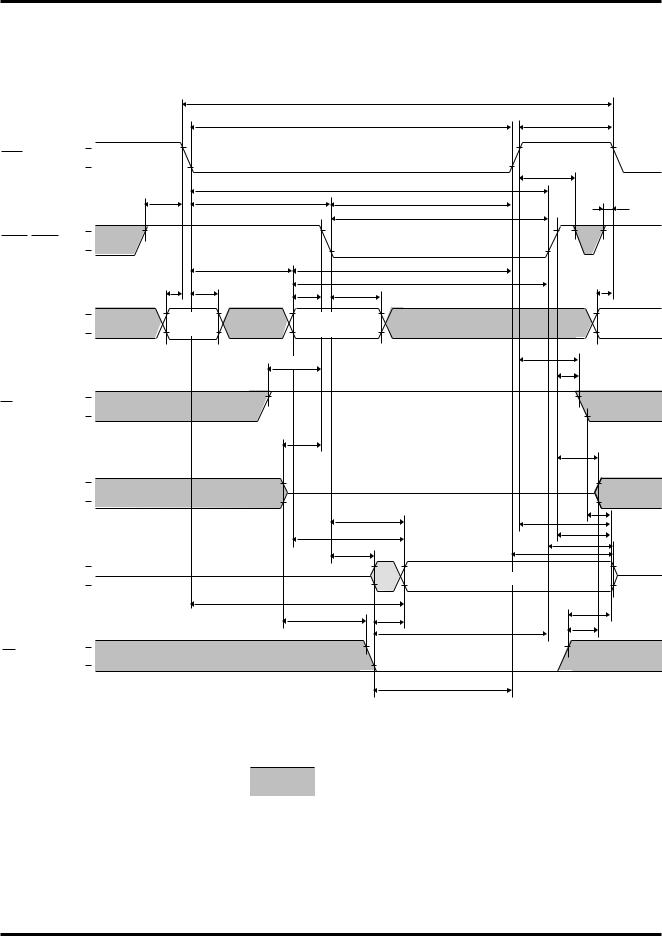
MITSUBISHI LSIs
M5M44265CJ,TP-5,-6,-7,-5S,-6S,-7S
EDO (HYPER PAGE MODE) 4194304-BIT (262144-WORD BY 16-BIT) DYNAMIC RAM
Timing Diagrams (Note 31)
Read Cycle
RAS
LCAS/UCAS
A0~A8
W
DQ1~DQ16 (INPUTS)
DQ1~DQ16
(OUTPUTS)
OE
VIH
VIL
VIH
VIL
VIH
VIL
VIH
VIL
VIH
VIL
VOH
VOL
VIH
VIL
|
|
|
tRC |
|
|
|
|
|
|
tRAS |
|
|
tRP |
|
|
|
|
|
tRPC |
|
tCRP |
|
|
tCSH |
|
|
|
|
tRCD |
|
|
tRSH |
tCRP |
|
|
|
|
|
|
tCAS |
|
|
|
|
|
|
|
|
|
|
tRAD |
|
tRAL |
|
|
tASR |
tRAH |
|
|
|
tCAL |
tASR |
tASC |
tCAH |
|
|
|||
|
|
|
|
|
||
|
ROW |
COLUMN |
|
|
ROW |
|
ADDRESS |
ADDRESS |
|
|
ADDRESS |
||
|
|
tRCS |
|
|
|
tRRH |
|
|
|
|
|
|
tRCH |
|
|
tDZC |
|
|
|
|
|
|
|
|
|
|
tCDD |
|
|
|
|
|
Hi-Z |
|
|
|
|
tCAC |
|
tREZ |
tWEZ |
|
|
|
tAA |
|
|
tOFF |
|
|
|
tCLZ |
|
tOHR |
tOHC |
|
|
|
|
|
||
|
|
Hi-Z |
tOEA |
DATA VALID |
Hi-Z |
|
|
|
|
|
|||
|
|
|
|
|
|
|
|
|
tRAC |
|
|
|
tOEZ |
|
|
tDZO |
|
tOEA |
|
|
|
|
|
|
tODD |
||
|
|
|
|
|
tOCH |
|
|
|
|
|
|
|
|
|
|
|
|
|
tORH |
|
Indicates the don't care input.
Note 31 |
|
VIH(min) ≤ VIN ≤ VIH(max) or VIL(min) ≤ VIN |
≤ VIL(max) |
|
|
||
|
|
Indicates the invalid output. |
|
|
|
|
|
|
|
|
|
8

MITSUBISHI LSIs
M5M44265CJ,TP-5,-6,-7,-5S,-6S,-7S
EDO (HYPER PAGE MODE) 4194304-BIT (262144-WORD BY 16-BIT) DYNAMIC RAM
Byte Read Cycle
|
|
|
|
|
tRC |
|
|
|
|
|
tRAS |
|
tRP |
RAS |
VIH |
|
|
|
tRPC |
|
VIL |
|
|
|
|
||
|
|
|
tCSH |
|
|
|
|
|
|
|
|
|
|
|
tCRP |
|
tRCD |
|
tRSH |
tCRP |
LCAS |
VIH |
|
|
|
|
|
|
|
|
|
|
|
|
(or UCAS) |
VIL |
|
|
|
|
|
|
|
|
|
|
tCAS |
tCPN |
UCAS |
VIH |
|
|
|
|
|
|
|
|
|
|
|
|
(or LCAS) |
VIL |
|
tRAD |
|
tRAL |
|
|
|
|
|
|
||
|
tASR |
tRAH |
|
|
tCAL |
|
|
tASC |
tCAH |
|
tASR |
||
|
|
|
|
|||
A0~A8 |
VIH |
ROW |
COLUMN |
|
ROW |
|
ADDRESS |
ADDRESS |
|
ADDRESS |
|||
|
|
|||||
|
VIL |
|
|
|
|
|
|
|
|
|
|
tRRH |
|
|
|
|
tRCS |
|
|
tRCH |
|
|
|
|
|
|
|
W |
VIH |
|
|
|
|
|
VIL |
|
|
|
|
|
|
|
|
|
|
|
|
|
DQ1~DQ8 |
VIH |
|
|
|
|
|
(or DQ9~DQ16) |
|
|
|
|
|
|
(INPUTS) |
VIL |
|
|
|
|
|
DQ1~DQ8 |
VOH |
|
|
|
Hi-Z |
|
|
|
|
|
|
||
(or DQ9~DQ16) |
|
|
|
|
|
|
(OUTPUTS) VOL |
|
|
|
|
|
|
|
|
|
tDZC |
|
|
tCDD |
|
|
|
|
|
|
|
DQ9~DQ16 |
|
|
|
|
Hi-Z |
|
(or DQ1~DQ8)VIH |
|
|
|
|
||
|
|
|
|
|
||
(INPUTS) |
VIL |
|
|
|
tREZ |
|
|
|
|
|
tCAC |
tWEZ |
|
|
|
|
|
tAA |
tOHR |
|
|
|
|
|
|
tOFF |
|
|
|
|
|
tCLZ |
|
|
|
|
|
|
|
tOHC |
|
DQ9~DQ16 |
VOH |
|
Hi-Z |
|
|
Hi-Z |
(or DQ1~DQ8) |
|
|
|
DATA VALID |
|
|
(OUTPUTS) VOL |
|
tRAC |
|
|
|
|
|
|
|
|
|
tOEZ |
|
|
|
|
tDZO |
|
tOEA |
|
|
|
|
|
|
||
|
|
|
|
|
tOCH |
tODD |
OE |
VIH |
|
|
|
|
|
VIL |
|
|
|
|
|
|
|
|
|
|
|
|
|
|
|
|
|
|
tORH |
|
9
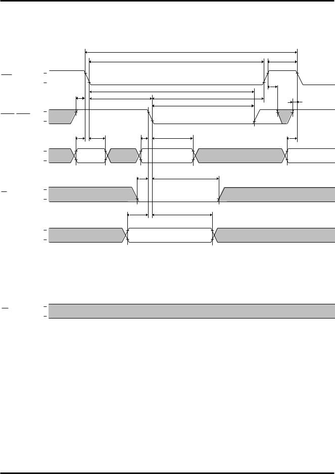
MITSUBISHI LSIs
M5M44265CJ,TP-5,-6,-7,-5S,-6S,-7S
EDO (HYPER PAGE MODE) 4194304-BIT (262144-WORD BY 16-BIT) DYNAMIC RAM
Early Write Cycle
VIH
RAS
VIL
VIH
LCAS/UCAS
VIL
VIH
A0~A8
VIL
VIH
W
VIL
DQ1~DQ16 VIH
(INPUTS) V
IL
|
|
|
tWC |
|
|
|
|
|
tRAS |
|
tRP |
|
|
|
|
|
tRPC |
tCRP |
|
|
tCSH |
|
|
|
tRCD |
|
tRSH |
tCRP |
|
|
|
|
|||
|
|
|
|
tCAS |
|
|
|
|
|
|
|
tASR |
tRAH |
tASC |
tCAH |
|
tASR |
|
|
|
|
|
|
|
ROW |
|
COLUMN |
|
ROW |
ADDRESS |
|
ADDRESS |
|
ADDRESS |
|
|
|
tWCS |
tWCH |
|
|
|
|
tDS |
tDH |
|
|
DATA VALID
DQ1~DQ16 VOH |
|
|
Hi-Z |
|
|||
(OUTPUTS) VOL |
|
|
|
|
|
VIH
OE
VIL
10
 Loading...