


 Loading...
PRELIMINARY |
|||||||
|
|
|
|
|
|
. . |
|
|
|
|
|
|
specification |
change |
|
|
|
|
|
|
|
to |
|
|
|
|
a |
final |
|
subject |
|
|
is |
not |
are |
|
|
||
|
|
|
|
||||
|
limits |
|
|
|
|||
This |
|
|
|
|
|||
|
|
|
|
|
|||
|
|
|
|
|
|
|
|
Notice:parametric |
|
|
|
|
|
||
Some |
|
|
|
|
|
|
|
DESCRIPTION
The 7534 Group is the 8-bit microcomputer based on the 740 family core technology.
The 7534 Group has a USB, 8-bit timers, and an A-D converter, and is useful for an input device for personal computer peripherals.
FEATURES
• Basic machine-language instructions ....................................... |
69 |
• The minimum instruction execution time .......................... |
0.34 μs |
(at 6 MHz oscillation frequency for the shortest instruction) |
|
• Memory size |
|
ROM ............................................... |
8K to 16K bytes |
RAM .............................................. |
256 to 384 bytes |
• Programmable I/O ports ...................................... |
28 (36-pin type) |
............................................................................ |
24 (32-pin type) |
• Interrupts............................................................................ |
33 (42-pin type) |
14 sources, 8 vectors |
|
• Timers ............................................................................ |
8-bit 3 |
PIN CONFIGURATION (TOP VIEW)
P12/SCLK |
|
|
|
|
|
|
|
|
|
|
|
|
|
|
|
|
|
1 |
|
||||
P13/SDATA |
|
|
|
|
|
|
|
|
|||
|
|
|
|
|
|
2 |
|
||||
P14/CNTR0 |
|
|
|
|
|
|
|
|
|||
|
|
|
|
|
|
3 |
|
||||
P20/AN0 |
|
|
|
|
|
|
|
|
|||
|
|
|
|
|
|
|
|
4 |
M37534E8FP |
||
|
|
|
|
|
|
||||||
P21/AN1 |
|
|
|
|
|
|
|
|
|
||
|
|
|
|
|
|
5 |
|
||||
P22/AN2 |
|
|
|
|
|
|
|
|
|||
|
|
|
|
|
|
6 |
|
||||
P23/AN3 |
|
|
|
|
|
|
|
|
|
||
|
|
|
|
|
|
|
7 |
|
|||
P24/AN4 |
|
|
|
|
|
|
|
|
|
||
8 |
|
||||||||||
|
|
|
|
|
|
|
|
||||
P25/AN5 |
|
|
|
|
|
|
|
|
|
|
|
|
|
|
|
|
|
9 |
|
||||
|
|
|
|
|
|
|
|||||
P26/AN6 |
|
|
|
|
|
|
|
|
|
|
|
10 |
|
||||||||||
|
|
|
|
|
|
|
|
|
|||
|
|
|
|
|
|
|
|
|
|
|
|
P27/AN7 |
|
|
|
|
|
|
11 |
|
|||
|
|
|
|
|
|
|
|||||
|
VREF |
|
|
|
|
|
|||||
12 |
|
||||||||||
|
|
|
|
|
|||||||
|
|
|
|
|
|
|
|
|
|
|
|
|
RESET |
|
|
|
|
|
|
|
|
|
|
|
|
|
|
|
|
13 |
|
||||
|
CNVSS |
|
|
|
|
|
|
||||
14 |
|
||||||||||
|
|
|
|
|
|
||||||
|
Vcc |
|
|
||||||||
15 |
|
||||||||||
|
XIN |
|
|
|
|
|
|
||||
16 |
|
||||||||||
|
|
|
|
|
|||||||
|
XOUT |
|
|
|
|
|
|
|
|||
17 |
|
||||||||||
|
|
|
|
|
|
||||||
|
|
|
|
|
|
|
|
|
|
|
|
|
VSS |
18 |
|
||||||||
|
|
|
|
|
|
|
|
|
|
|
|
MITSUBISHI MICROCOMPUTERS
7534 Group
SINGLE-CHIP 8-BIT CMOS MICROCOMPUTER
• Serial I/O1 ................................ |
used only for Low Speed in USB |
|
(based on USBSpec. Rev.1.1) |
• Serial I/O2 |
(USB/UART) |
8-bit 1 |
|
• A-D converter |
(Clock-synchronized) |
10-bit 8 channels |
|
• Clock generating circuit ............................................. |
Built-in type |
(connect to external ceramic resonator or quartz-crystal oscillator )
• Watchdog timer ............................................................ 16-bit 1
•Power source voltage
At 6 MHz XIN oscillation frequency at ceramic resonator
................................ 4.1 to 5.5 V(4.4 to 5.25 V at USB operation)
• Power dissipation ............................................ |
30 mW (standard) |
• Operating temperature range ................................... |
–20 to 85 °C |
|
(0 to 70 °C at USB operation) |
•Built-in USB 3.3 V Regulator + transceiver based on USB Spec. Rev.1.1
APPLICATION
Input device for personal computer peripherals
|
|
|
|
|
|
P11/TXD/D+ |
|
36 |
|
|
|
|
|
|
|
|
|
|
|
P10/RXD/D- |
|
35 |
|
|
|
|
|
|
|
|
|
|
|
P07 |
|
34 |
|
|
|
|
|
|
|
|
|
|
|
P06 |
M37534M4 |
33 |
|
|
|
|
|
|
|
|
|
|
P00 |
|
27 |
|
|
|
|
||
|
32 |
|
|
|
|
P05 |
|
31 |
|
|
|
|
P04 |
|
30 |
|
|
|
|
P03 |
|
|
|
|
|
|
P02 |
|
29 |
|
|
|
|
|
|
|
|
|
|
|
P01 |
- |
28 |
|
|
|
|
|
|
|
|
|
|
|
|
|
|
|
|
|
|
|
|
|
|
|
|
|
|
XXXFP |
26 |
|
|
|
|
USBVREFOUT |
|
|
|
|
|
P37/INT0 |
|
25 |
|
|
|
|
||
|
|
|
|
|
||
|
|
|
|
|
|
P35(LED5) |
|
24 |
|
|
|
|
|
|
|
|
|
|
||
|
|
|
|
|
|
P34(LED4) |
|
23 |
|
|
|
|
|
|
|
|
|
|
|
P33(LED3) |
|
22 |
|
|
|
|
|
|
|
|
|
|
|
P32(LED2) |
|
21 |
|
|
|
|
|
|
|
|
|
|
|
|
|
20 |
|
|
|
|
P31(LED1) |
|
|
|
|
|
|
|
|
19 |
|
|
|
|
P30(LED0) |
|
|
|
|
|
||
|
|
|
|
|
|
|
Package type: 36P2R-A
Fig. 1 Pin configuration of M37534M4-XXXFP, M37534E8FP
|
|
|
|
|
|
Y |
||
PRELIMINAR |
. . |
|||||||
|
|
|
|
|
specification |
change |
||
|
|
|
|
|
|
|
to |
|
|
|
|
a |
final |
|
subject |
|
|
|
is |
not |
are |
|
|
|
||
|
|
|
|
|
||||
|
limits |
|
|
|
|
|||
This |
|
|
|
|
|
|||
|
|
|
|
|
|
|||
|
|
|
|
|
|
|
|
|
Notice:parametric |
|
|
|
|
|
|
||
Some |
|
|
|
|
|
|
|
|
MITSUBISHI MICROCOMPUTERS
7534 Group
SINGLE-CHIP 8-BIT CMOS MICROCOMPUTER
PIN CONFIGURATION (TOP VIEW)
|
|
|
|
|
P06 |
P05 |
P04 |
P03 |
P02 |
|
P01 |
|
P00 |
USBVREFOUT |
|
|
|
|
|
|
|||||||||||||||||
|
|
|
|
|
|
|
|
|
|
|
|
|
|
|
|
|
|
|
|
|
|
|
|
|
|
|
|
|
|
|
|
|
|
|
|
||
|
|
|
|
|
|
|
|
|
|
|
|
|
|
|
|
|
|
|
|
|
|
|
|
|
|
|
|
|
|
|
|
|
|
|
|
|
|
|
|
|
|
|
|
|
|
|
|
|
|
|
|
|
|
|
|
|
|
|
|
|
|
|
|
|
|
|
|
|
|
|
|
|
|
|
|
|
|
|
|
|
|
|
|
|
|
|
|
|
|
|
|
|
|
|
|
|
|
|
|
|
|
|
|
|
|
|
|
|
|
|
|
|
|
|
|
|
|
|
24 |
|
23 |
|
22 |
|
21 |
|
20 |
|
|
19 |
|
18 |
|
17 |
|
|
|
|
|
|
|
|
|||||||||
P07 |
|
|
|
|
|
|
|
|
|
|
|
|
|
|
|
|
|
|
|
|
|
|
|
|
|
|
|
|
|
|
|
|
|
|
|
P34(LED4) |
|
|
|
|
|
|
|
|
|
|
|
|
|
|
|
|
|
|
|
|
|
|
|
|
|
|
|
|
|
|
|
|
|
|
|
|
|||
25 |
|
|
|
|
|
|
|
|
|
|
|
|
|
|
|
|
|
|
|
|
|
|
|
|
|
|
16 |
|
|
|
|
|
|||||
|
|
|
|
|
|
|
|
|
|
|
|
|
|
|
|
|
|
|
|
|
|
|
|
|
|
|
|
|
|||||||||
|
|
|
|
|
|
|
|
|
|
|
|
|
|
|
|
|
|
|
|
|
|
|
|
|
|||||||||||||
P10/RXD/D- |
|
|
26 |
|
|
|
|
|
|
|
|
|
|
|
|
|
|
|
|
|
|
|
|
|
|
|
|
|
|
15 |
|
|
|
|
|
P33(LED3) |
|
|
|
|
|
|
|
|
|
|
|
|
|
|
|
|
|
|
|
|
|
|
|
|
|
|
|
|
|
|
|||||||||
|
|
|
|
|
|
|
|
|
|
|
|
|
|
|
|
|
|
|
|
|
|
|
|
|
|||||||||||||
P11/TXD/D+ |
|
|
27 |
|
|
|
|
|
|
|
|
|
|
|
|
|
|
|
|
|
|
|
|
|
|
|
|
|
14 |
|
|
|
|
|
P32(LED2) |
||
|
|
|
|
|
|
|
|
|
|
|
|
|
|
|
|
|
|
|
|
|
|
|
|
|
|
|
|
||||||||||
|
|
|
|
|
|
|
|
|
|
|
|
|
|
|
|
|
|
|
|
|
|
|
|
|
|||||||||||||
P12/SCLK |
|
|
28 |
M37534M4-XXXGP |
13 |
|
|
|
|
|
P31(LED1) |
||||||||||||||||||||||||||
|
|
|
|||||||||||||||||||||||||||||||||||
|
|
||||||||||||||||||||||||||||||||||||
P13/SDATA |
|
|
29 |
12 |
|
|
|
|
|
P30(LED0) |
|||||||||||||||||||||||||||
|
|
|
|
|
|
|
|
|
|
|
|
|
|
|
|
|
|
|
|
|
|
|
|
|
|
|
|
|
|
|
|
|
|||||
|
|
|
|
|
|
|
|
|
|
|
|
|
|
|
|
|
|
|
|
|
|
|
|
|
|
|
|
|
|
|
|
||||||
P14/CNTR0 |
|
|
|
|
|
|
|
|
|
|
|
|
|
|
|
|
|
|
|
|
|
|
|
|
|
|
|
|
|
|
|
|
|
|
|
VSS |
|
30 |
|
|
|
|
|
|
|
|
|
|
|
|
|
|
|
|
|
|
|
|
|
|
|
|
|
|
11 |
|
|
|
|
|
|||||
|
|
|
|
|
|
|
|
|
|
|
|
|
|
|
|
|
|
|
|
|
|
|
|
|
|
|
|||||||||||
|
|
|
|
|
|
|
|
|
|
|
|
|
|
|
|
|
|
|
|
|
|
|
|
|
|||||||||||||
P20/AN0 |
|
|
31 |
|
|
|
|
|
|
|
|
|
|
|
|
|
|
|
|
|
|
|
|
|
|
|
|
|
|
10 |
|
|
|
|
|
XOUT |
|
|
|
|
|
|
|
|
|
|
|
|
|
|
|
|
|
|
|
|
|
|
|
|
|
|
|
|
|
|
|
|
|
|
|||||
|
|
|
|
|
|
|
|
|
|
|
|
|
|
|
|
|
|
|
|
|
|
|
|
|
|||||||||||||
P21/AN1 |
|
|
32 |
|
|
|
|
|
|
|
|
|
|
|
|
|
|
|
|
|
|
|
|
|
|
|
|
|
|
9 |
|
|
|
|
|
XIN |
|
|
|
|
|
|
|
|
|
|
|
|
|
|
|
|
|
|
|
|
|
|
|
|
|
|
|
|
|||||||||||
|
|
|
|
|
|
|
|
|
|
|
|
|
|
|
|
|
|
|
|
|
|
|
|
|
|
|
|
|
|
|
|
|
|||||
|
|
|
|
|
|
|
|
|
|
|
|
|
|
|
|
|
|
|
|
|
|
|
|
|
|
|
|
|
|
|
|
|
|
|
|
||
|
|
|
|
|
1 |
|
2 |
|
3 |
|
4 |
|
5 |
|
|
6 |
|
7 |
|
8 |
|
|
|
|
|
|
|
|
|||||||||
|
|
|
|
|
|
|
|
|
|
|
|
|
|
|
|
|
|
|
|
|
|
|
|
|
|
|
|
|
|
|
|
|
|
|
|
|
|
|
|
|
|
|
|
|
|
|
|
|
|
|
|
|
|
|
|
|
|
VCC |
|
|
|
|
|
|
|||||||||||
|
|
|
|
|
|
|
|
|
|
|
|
|
|
|
|
|
|
|
|
|
|
|
|
|
|
|
|||||||||||
|
|
|
|
|
|
|
|
|
|
|
|
|
|
|
|
|
|
|
|
|
|
|
|
||||||||||||||
|
|
|
|
|
P22/AN2 |
P23/AN3 |
P24/AN4 |
P25/AN5 |
VREF |
|
RESET |
|
CNVSS |
|
|
|
|
|
|
||||||||||||||||||
|
|
|
|
|
|
|
|
|
|
|
|
|
|||||||||||||||||||||||||
|
|
|
|
|
|
|
|
|
|
|
|
|
|
|
|
|
|
|
|
|
|
|
|
|
|||||||||||||
Outline 32P6U-A
Fig. 2 Pin configuration of M37534M4-XXXGP
2
PRELIMINARY |
|||||||
|
|
|
|
|
|
. . |
|
|
|
|
|
|
specification |
change |
|
|
|
|
|
|
|
to |
|
|
|
|
a |
final |
|
subject |
|
|
is |
not |
are |
|
|
||
|
|
|
|
||||
|
limits |
|
|
|
|||
This |
|
|
|
|
|||
|
|
|
|
|
|||
|
|
|
|
|
|
|
|
Notice:parametric |
|
|
|
|
|
||
Some |
|
|
|
|
|
|
|
PIN CONFIGURATION (TOP VIEW)
MITSUBISHI MICROCOMPUTERS
7534 Group
SINGLE-CHIP 8-BIT CMOS MICROCOMPUTER
P14/CNTR0 
 1
1
P15 

 2
2
P16 

 3
3
P20/AN0 

 4
4
P21/AN1 

 5 NC 6 P22/AN2

 7 P23/AN3

 8 P24/AN4

 9 P25/AN5

 10 P26/AN6

 11 P27/AN7

 12
12
P40 

 13
13
P41 

 14
14
VREF 
 15
15
RESET 
 16
16
CNVSS 
 17
17
Vcc 18
XIN  19
19
XOUT 
 20
20
VSS 21
M37534RSS XXXSP-M37534M4 M37534E8SP
|
|
|
|
|
|
|
P13/SDATA |
|
42 |
|
|
|
|
|
|
||
|
|
|
|
|
|
|||
|
|
|
|
|
|
|
P12/SCLK |
|
41 |
|
|
|
|
|
|
||
|
|
|
|
|
|
|||
|
|
|
|
|
|
|
P11/TXD/D+ |
|
40 |
||||||||
|
|
|
|
|
|
|||
|
|
|
|
|
|
|
P10/RXD/D- |
|
39 |
||||||||
|
|
|
|
|
|
|||
|
|
|
|
|
|
|
P07 |
|
38 |
||||||||
|
|
|
|
|
|
|||
|
|
|
|
|
|
|
P06 |
|
37 |
||||||||
|
|
|
|
|
|
|||
|
|
|
|
|
|
|
P05 |
|
36 |
|
|
|
|
|
|
||
|
|
|
|
|
|
|
P04 |
|
35 |
|
|
|
|
|
|
||
|
|
|
|
|
|
|
P03 |
|
34 |
|
|
|
|
|
|
||
|
|
|
|
|
|
|
P02 |
|
33 |
|
|
|
|
|
|
||
|
|
|
|
|
|
|
P01 |
|
32 |
||||||||
|
|
|
|
|
|
|||
|
|
|
|
|
|
|
P00 |
|
31 |
|
|
|
|
|
|
||
|
|
|
|
|
|
|||
|
|
|
|
|
|
|
USBVREFOUT |
|
30 |
||||||||
|
|
|
|
|
|
|||
|
|
|
|
|
|
|
P37/INT0 |
|
29 |
||||||||
|
|
|
|
|
|
|||
|
|
|
|
|
|
|
P36(LED6)/INT1 |
|
28 |
|
|
|
|
|
|
||
|
|
|
|
|
|
|
P35(LED5) |
|
27 |
|
|
|
|
|
|
||
|
|
|
|
|
|
|
|
|
26 |
|
|
|
|
|
|
P34(LED4) |
|
|
|
|
|
|
|
|||
|
|
|
|
|
|
|
P33(LED3) |
|
25 |
|
|
|
|
|
|
||
|
|
|
|
|
|
|||
|
|
|
|
|
|
|
P32(LED2) |
|
24 |
|
|
|
|
|
|
||
|
|
|
|
|
|
|||
|
|
|
|
|
|
|
P31(LED1) |
|
23 |
|
|
|
|
|
|
||
|
|
|
|
|
|
|||
|
|
|
|
|
|
|
P30(LED0) |
|
22 |
|
|
|
|
|
|
||
|
|
|
|
|
|
|
|
Outline 42S1M, 42P4B
Fig. 3 Pin configuration of M37534RSS, M37534M4-XXXSP, M37534E8SP
3
PRELIMINARY |
|||||||
|
|
|
|
|
|
. . |
|
|
|
|
|
|
specification |
change |
|
|
|
|
|
|
|
to |
|
|
|
|
a |
final |
|
subject |
|
|
is |
not |
are |
|
|
||
|
|
|
|
||||
|
limits |
|
|
|
|||
This |
|
|
|
|
|||
|
|
|
|
|
|||
|
|
|
|
|
|
|
|
Notice:parametric |
|
|
|
|
|
||
Some |
|
|
|
|
|
|
|
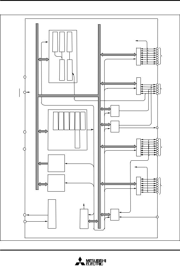
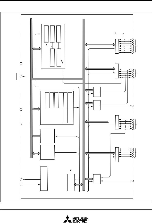
FUNCTIONAL BLOCK
MITSUBISHI MICROCOMPUTERS
7534 Group
SINGLE-CHIP 8-BIT CMOS MICROCOMPUTER
FUNCTIONAL BLOCK DIAGRAM (Package: 36P2R)
|
|
|
(8) |
(8) |
(8) |
|
Key-onwakeup |
|
|
|
|
|
Timer 1 |
Timer 2 |
Timer X |
|
|
27 |
I/O port P0 |
|
|
|
|
12 (8) |
|
|
P0(8) |
32 31 30 29 28 |
|
|
|
|
|
X (8) |
|
|
34 33 |
|
|
|
CNVSS |
14 |
|
Prescaler |
Prescaler |
|
|
|
|
Reset input |
RESET |
13 |
|
|
|
|
P1(5) |
3 2 1 36 35 |
I/O port P1 |
|
|
|
|
|
|
SI/O2(8) |
|
|
|
|
VCC |
15 |
|
|
|
SI/O1(8) USB(LS) |
USBVREFOUT |
4 |
|
|
|
|
|
|
|
|
|
26 |
|
|
|
|
|
|
|
|
P2(8) |
6 5 |
P2 |
|
VSS |
18 |
|
|
|
|
10 9 8 7 |
I/O port |
|
|
|
|
|
|
|
|
|
11 |
|
|
|
|
|
|
|
|
INT0 |
|
|
|
|
|
|
|
|
|
P3(7) |
24 23 22 21 20 19 |
I/O port P3 |
|
|
|
|
|
|
|
|
25 |
|
Clock input Clock output |
XIN XOUT |
16 17 |
Clock generating circuit |
|
Watchdog timer Reset |
A-D converter (10) |
|
12 |
VREF |
Fig. 4 Functional block diagram (36P2R package type)
4
|
|
|
|
|
|
Y |
||
PRELIMINAR |
. . |
|||||||
|
|
|
|
|
specification |
change |
||
|
|
|
|
|
|
|
to |
|
|
|
|
a |
final |
|
subject |
|
|
|
is |
not |
are |
|
|
|
||
|
|
|
|
|
||||
|
limits |
|
|
|
|
|||
This |
|
|
|
|
|
|||
|
|
|
|
|
|
|||
|
|
|
|
|
|
|
|
|
Notice:parametric |
|
|
|
|
|
|
||
Some |
|
|
|
|
|
|
|
|
MITSUBISHI MICROCOMPUTERS
7534 Group
SINGLE-CHIP 8-BIT CMOS MICROCOMPUTER
|
|
Timer1(8) |
Timer2(8) |
TimerX(8) |
|
CNVSS |
7 |
Prescaler12(8) |
PrescalerX(8) |
Resetinput |
RESET |
6 |
|
|
VCC |
8 |
32P6U-A) |
|
VSS |
11 |
|
|
FUNCTIONALBLOCKDIAGRAM(Package: |
Clockinput Clockoutput |
XXINOUT |
9 10 |
Clockgeneratingcircuit |
Watchdogtimer Reset |
Fig. 5 Functional block diagram (32P6U-A package type)
Key-onwakeup |
|
|
P0(8) |
232221201918 |
I/OportP0 |
|
2524 |
|
P1(5) |
282726 |
portP1 |
|
3029 |
I/O |
SI/O2(8)
SI/O1(8) |
USB(LS) |
USBVREFOUT
 P2(6)
P2(6)
17 |
|
3231 |
P2 |
2 1 |
port |
4 3 |
I/O |
P3(5) |
1615141312 |
I/OportP3 |
A-D converter (10) |
5 |
VREF |
5

PRELIMINARY |
|||||||
|
|
|
|
|
|
. . |
|
|
|
|
|
|
specification |
change |
|
|
|
|
|
|
|
to |
|
|
|
|
a |
final |
|
subject |
|
|
is |
not |
are |
|
|
||
|
|
|
|
||||
|
limits |
|
|
|
|||
This |
|
|
|
|
|||
|
|
|
|
|
|||
|
|
|
|
|
|
|
|
Notice:parametric |
|
|
|
|
|
||
Some |
|
|
|
|
|
|
|
MITSUBISHI MICROCOMPUTERS
7534 Group
SINGLE-CHIP 8-BIT CMOS MICROCOMPUTER
|
CNVSS |
17 |
Reset input |
RESET |
16 |
VCC |
18 |
VSS |
21 |
wakeup on-Key |
|
|
P0(8) |
35 34 33 32 31 |
port P0 |
|
37 36 |
I/O |
|
38 |
|
|
39 |
|
P1(7) |
2 1 42 41 40 |
I/O port P1 |
|
3 |
|
SI/O2(8) |
|
|
SI/O1(8) USB(LS) |
30 |
USBVREFOUT |
|
4 |
|
|
5 |
I/O port P2 |
P2(8) |
11 10 9 8 7 |
|
|
12 |
|
INT1 |
|
|
INT0 |
|
|
P3(8) |
28 27 26 25 24 23 22 |
I/O port P3 |
|
29 |
|
Clock input Clock output X IN X OUT |
19 20 |
Clock generating circuit |
Watchdog timer Reset |
A-D converter (10) |
P4(2) |
13 14 15 |
VREF |
I/O port P4 |
Fig. 6 Functional block diagram (42P4B package type)
6

PRELIMINARY |
|||||||
|
|
|
|
|
|
. . |
|
|
|
|
|
|
specification |
change |
|
|
|
|
|
|
|
to |
|
|
|
|
a |
final |
|
subject |
|
|
is |
not |
are |
|
|
||
|
|
|
|
||||
|
limits |
|
|
|
|||
This |
|
|
|
|
|||
|
|
|
|
|
|||
|
|
|
|
|
|
|
|
Notice:parametric |
|
|
|
|
|
||
Some |
|
|
|
|
|
|
|
MITSUBISHI MICROCOMPUTERS
7534 Group
SINGLE-CHIP 8-BIT CMOS MICROCOMPUTER
PIN DESCRIPTION
Table 1 Pin description
|
Pin |
Name |
|
|
|
Function |
|
|
||
|
|
|
|
|
Function expect a port function |
|||||
|
Vcc, Vss |
Power source |
•Apply voltage of 4.1 to 5.5 V to Vcc, and 0 V to Vss. |
|
||||||
|
|
|
|
|
|
|
|
|||
|
VREF |
Analog reference |
•Reference voltage input pin for A-D converter |
|
||||||
|
|
|
voltage |
|
|
|
|
|
|
|
|
|
|
|
|
|
|
|
|||
|
USBVREFOUT |
USB reference |
•Output pin for pulling up a D- line with 1.5 kΩ external resistor |
|
||||||
|
|
|
voltage output |
|
|
|
|
|
|
|
|
|
|
|
|
|
|
|
|||
|
CNVss |
CNVss |
•Chip operating mode control pin, which is always connected to Vss. |
|
||||||
|
|
|
|
|
|
|
|
|||
|
|
|
Reset input |
•Reset input pin for active “L” |
|
|||||
|
RESET |
|
||||||||
|
|
|
|
|
|
|
|
|||
|
XIN |
Clock input |
•Input and output pins for main clock generating circuit |
|
||||||
|
|
|
|
•Connect a ceramic resonator or quartz crystal oscillator between the XIN and XOUT pins. |
||||||
|
XOUT |
Clock output |
||||||||
|
•If an external clock is used, connect the clock source to the XIN pin and leave the XOUT pin open. |
|||||||||
|
|
|
|
|||||||
|
|
|
|
|
|
|
||||
|
P00–P07 |
I/O port P0 |
•8-bit I/O port. |
|
•Key-input (key-on wake up |
|||||
|
|
|
|
•I/O direction register allows each pin to be individually pro- |
|
interrupt input) pins |
||||
|
|
|
|
|
|
|||||
|
|
|
|
grammed as either input or output. |
|
|
||||
|
|
|
|
•CMOS compatible input level |
|
|
||||
|
|
|
|
•CMOS 3-state output structure |
|
|
||||
|
|
|
|
•Whether a built-in pull-up resistor is to be used or not can be |
|
|
||||
|
|
|
|
determined by program. |
|
|
||||
|
|
|
|
|
|
|
||||
|
P10/RxD/D- |
I/O port P1 |
•7-bit I/O port |
|
•Serial I/O1 function pin |
|||||
|
P11/TxD/D+ |
|
•I/O direction register allows each pin to be individually pro- |
|
|
|||||
|
|
|
|
grammed as either input or output. |
|
|
||||
|
P12/SCLK |
|
|
•Serial I/O2 function pin |
||||||
|
|
•CMOS compatible input level |
|
|||||||
|
P13/SDATA |
|
|
|
||||||
|
|
|
|
|
|
|
|
|
||
|
|
|
|
•CMOS 3-state output structure |
|
|
||||
|
P14/CNTR0 |
|
|
•Timer X function pin |
||||||
|
|
•CMOS/TTL level can be switched for P10, P12, P13. |
|
|||||||
|
|
|
|
|
|
|||||
|
|
|
|
•When using the USB function, input level of ports P10 and |
|
|
||||
|
|
|
|
P11 becomes USB input level, and output level of them |
|
|
||||
|
P15, P16 |
|
|
|
||||||
|
|
becomes USB output level. |
|
|
||||||
|
|
|
|
|
|
|||||
|
|
|
|
|
|
|
||||
|
P20/AN0– |
I/O port P2 |
•8-bit I/O port having almost the same function as P0 |
|
•Input pins for A-D converter |
|||||
|
P27/AN7 |
|
•CMOS compatible input level |
|
|
|||||
|
|
|
|
|
|
|||||
|
|
|
|
•CMOS 3-state output structure |
|
|
||||
|
|
|
|
|
|
|
||||
|
P30–P35 |
I/O port P3 |
•8-bit I/O port |
|
||||||
|
|
|
|
•I/O direction register allows each pin to be individually programmed as either input or output. |
||||||
|
|
|
|
•CMOS compatible input level (CMOS/TTL level can be switched for P36, P37). |
||||||
|
|
|
|
•CMOS 3-state output structure |
|
|||||
|
|
|
|
•P30 to P36 can output a large current for driving LED. |
|
|||||
|
|
|
•Whether a built-in pull-up resistor is to be used or not can be |
|
|
|
||||
|
P36/INT1 |
|
|
•Interrupt input pins |
||||||
|
P37/INT0 |
|
determined by program. |
|
|
|||||
|
|
|
|
|||||||
|
P40, P41 |
I/O port P4 |
•2-bit I/O port |
|
||||||
|
|
|
|
•I/O direction register allows each pin to be individually programmed as either input or output. |
||||||
|
|
|
|
|
|
|
|
|
|
|
|
|
|
|
|
|
|
|
|
|
|
|
|
|
|
|
|
|
|
|
|
|
|
|
|
|
|
|
|
|
|
|
|
7
|
|
|
|
|
|
Y |
||
PRELIMINAR |
. . |
|||||||
|
|
|
|
|
specification |
change |
||
|
|
|
|
|
|
|
to |
|
|
|
|
a |
final |
|
subject |
|
|
|
is |
not |
are |
|
|
|
||
|
|
|
|
|
||||
|
limits |
|
|
|
|
|||
This |
|
|
|
|
|
|||
|
|
|
|
|
|
|||
|
|
|
|
|
|
|
|
|
Notice:parametric |
|
|
|
|
|
|
||
Some |
|
|
|
|
|
|
|
|
MITSUBISHI MICROCOMPUTERS
7534 Group
SINGLE-CHIP 8-BIT CMOS MICROCOMPUTER
GROUP EXPANSION
Mitsubishi plans to expand the 7534 group as follow:
Memory type
Support for Mask ROM version, One Time PROM version, and Emulator MCU .
Memory size |
|
ROM/PROM size .................................................. |
8 K to 16 K bytes |
RAM size ................................................................ |
256 to 384 bytes |
Package |
|
36P2R-A |
..................................... 0.8 mm-pitch plastic molded SOP |
32P6U-A ................................... |
0.8 mm-pitch plastic molded LQFP |
42P4B ................................................... |
42 pin plastic molded SDIP |
42SIM ...................................... |
42 pin shrink ceramic PIGGY BACK |
ROM size (Byte)
16K |
M37534E8 |
8K |
M37534M4 |
0 |
128 |
256 |
384 RAM size |
|
|
|
(Byte) |
Fig. 7 Memory expansion plan
Currently supported products are listed below.
Table 2 List of supported products
Product |
(P) ROM size (bytes) |
RAM size |
|
Package |
Remarks |
|||||
ROM size for User () |
(bytes) |
|
||||||||
M37534M4-XXXFP |
8192 |
(8062) |
256 |
|
36P2R-A |
Mask ROM version |
||||
M37534M4-XXXGP |
8192 |
(8062) |
256 |
|
32P6U-A |
Mask ROM version |
||||
|
|
|
|
|
|
|
|
|
|
|
M37534M4-XXXSP |
8192 |
(8062) |
256 |
|
|
42P4B |
Mask ROM version |
|||
|
|
|
|
|
|
|
|
|
||
M37534E8FP |
16384 |
(16254) |
384 |
|
36P2R-A |
One Time PROM version (blank) |
||||
|
|
|
|
|
|
|
|
|||
M37534E8SP |
16384 |
(16254) |
384 |
|
|
42P4B |
One Time PROM version (blank) |
|||
|
|
|
|
|
|
|
|
|
|
|
M37534RSS |
|
|
|
|
384 |
|
|
42S1M |
Emulator MCU |
|
|
|
|
|
|
|
|||||
|
|
|
|
|
|
|
|
|
|
|
|
|
|
|
|
|
|
|
|
|
|
|
|
|
|
|
|
|
|
|
|
|
8
PRELIMINARY |
|||||||
|
|
|
|
|
|
. . |
|
|
|
|
|
|
specification |
change |
|
|
|
|
|
|
|
to |
|
|
|
|
a |
final |
|
subject |
|
|
is |
not |
are |
|
|
||
|
|
|
|
||||
|
limits |
|
|
|
|||
This |
|
|
|
|
|||
|
|
|
|
|
|||
|
|
|
|
|
|
|
|
Notice:parametric |
|
|
|
|
|
||
Some |
|
|
|
|
|
|
|
MITSUBISHI MICROCOMPUTERS
7534 Group
SINGLE-CHIP 8-BIT CMOS MICROCOMPUTER
FUNCTIONAL DESCRIPTION |
[CPU Mode Register] CPUM |
Central Processing Unit (CPU)
The 7534 Group uses the standard 740 family instruction set. Refer to the table of 740 family addressing modes and machine-language instructions or the 740 Family Software Manual for details on each instruction set.
Machine-resident 740 family instructions are as follows:
1.The FST and SLW instructions cannot be used.
2.The MUL and DIV instructions cannot be used.
3.The WIT instruction can be used.
4.The STP instruction can be used.
The CPU mode register contains the stack page selection bit. This register is allocated at address 003B16.
b7 |
b0 |
CPU mode register (CPUM: address 003B 16)
Processor mode bits
b1 |
b0 |
|
|
0 |
0 |
Single-chip mode |
|
0 |
1 |
|
|
|
|
||
1 |
0 |
|
Not available |
1 |
1 |
|
|
|
|
||
Stack page selection bit |
|||
0 |
: 0 page |
||
1 |
: 1 page |
||
Not used (returns “0” when read) (Do not write “1” to these bits )
Main clock division ratio selection bits
b7 |
b6 |
: f(φ) = f(XIN)/2 (High-speed mode) |
0 |
0 |
|
0 |
1 |
: f(φ) = f(XIN)/8 (Middle-speed mode) |
1 |
0 |
: applied from ring oscillator |
1 |
1 |
: f(φ) = f(XIN) (Double-speed mode) |
Fig. 8 Structure of CPU mode register
Switching method of CPU mode register
Switch the CPU mode register (CPUM) at the head of program after releasing Reset in the following method.
After releasing reset
Wait until establish ceramic oscillator clock.
Switch the clock division ratio selection bits (bits 6 and 7 of CPUM)
Start with a built-in ring oscillator (Note)
Switch to other mode except a ring oscillator (Select one of 1/1, 1/2, and 1/8)
Main routine
Note. After releasing reset the operation starts by starting a ring oscillator automatically.
Do not use a ring oscillator at ordinary operation.
Fig. 9 Switching method of CPU mode register
9

PRELIMINARY |
|||||||
|
|
|
|
|
|
. . |
|
|
|
|
|
|
specification |
change |
|
|
|
|
|
|
|
to |
|
|
|
|
a |
final |
|
subject |
|
|
is |
not |
are |
|
|
||
|
|
|
|
||||
|
limits |
|
|
|
|||
This |
|
|
|
|
|||
|
|
|
|
|
|||
|
|
|
|
|
|
|
|
Notice:parametric |
|
|
|
|
|
||
Some |
|
|
|
|
|
|
|
MITSUBISHI MICROCOMPUTERS
7534 Group
SINGLE-CHIP 8-BIT CMOS MICROCOMPUTER
Memory
Special function register (SFR) area
The SFR area in the zero page contains control registers such as I/O ports and timers.
RAM
RAM is used for data storage and for a stack area of subroutine calls and interrupts.
Zero page
The 256 bytes from addresses 000016 to 00FF16 are called the zero page area. The internal RAM and the special function registers (SFR) are allocated to this area.
The zero page addressing mode can be used to specify memory and register addresses in the zero page area. Access to this area with only 2 bytes is possible in the zero page addressing mode.
Special page
ROM
The first 128 bytes and the last 2 bytes of ROM are reserved for device testing and the rest is a user area for storing programs.
Interrupt vector area
The interrupt vector area contains reset and interrupt vectors.
The 256 bytes from addresses FF0016 to FFFF16 are called the special page area. The special page addressing mode can be used to specify memory addresses in the special page area. Access to this area with only 2 bytes is possible in the special page addressing mode.
|
|
|
|
|
000016 |
SFR area |
|
|
|
||
|
|
|
|
|
|
|
|
|
|
|
|
|
|
|
|
|
|
|
|
|
|
|
Zero page |
|
|
|
|
|
004016 |
|
|
|
|||
|
|
|
|
|
|
|
|
|
|||
|
|
|
|
RAM |
010016 |
|
|
|
|
||
|
|
|
|
|
|
|
|
||||
|
|
|
|
|
|
|
|
|
|
|
|
|
|
RAM area |
|
|
|
|
|
|
|
|
|
|
|
|
|
|
|
|
|
|
|
|
|
|
|
RAM capacity |
address |
|
|
|
XXXX16 |
|
|
|
|
|
|
(bytes) |
XXXX16 |
|
|
|
|
|
|
|
|
|
|
|
|
|
|
|
|
|
|
|
|
|
|
256 |
013F16 |
|
|
|
|
Reserved area |
|
|
|
|
|
384 |
01BF16 |
|
|
|
|
|
|
|
|
|
|
|
|
|
044016 |
|
|
|
|
||
|
|
|
|
|
Not used |
|
|
|
|||
|
|
|
|
|
|
|
|
|
|
|
|
|
|
|
|
|
|
|
YYYY16 |
|
|
|
|
|
|
|
|
|
|
|
Reserved ROM area |
|
|
|
|
|
|
|
|
|
|
|
|
|
|
|
|
|
|
|
|
|
|
|
|
(128 bytes) |
|
|
|
|
|
|
|
ROM |
|
|
ZZZZ16 |
|
|
|
|
|
|
|
|
|
|
|
|
|
|
||
|
|
|
|
|
|
|
|
|
|
|
|
ROM area |
|
|
|
|
|
FF0016 |
|
|
|
|
|
|
|
|
|
|
|
|
|
|
|||
|
|
|
|
|
|
|
|
|
|
||
ROM capacity |
|
address |
address |
|
|
|
|
|
|
|
|
(bytes) |
|
YYYY16 |
ZZZZ16 |
|
|
|
FFEC16 |
|
|
|
Special page |
|
|
|
|
|
|
|
|
|
|
||
8192 |
|
E00016 |
E08016 |
|
|
|
Interrupt vector area |
|
|
|
|
|
|
|
|
|
|
|
|
||||
16384 |
|
C00016 |
C08016 |
|
|
|
FFFE16 |
|
|
|
|
|
|
|
|
|
|
|
Reserved ROM area |
|
|
|
|
|
|
|
|
|
|
|
|
||||
|
|
|
|
|
|
|
FFFF16 |
|
|
|
|
Fig. 10 Memory map diagram
10
PRELIMINARY |
|||||||
|
|
|
|
|
|
. . |
|
|
|
|
|
|
specification |
change |
|
|
|
|
|
|
|
to |
|
|
|
|
a |
final |
|
subject |
|
|
is |
not |
are |
|
|
||
|
|
|
|
||||
|
limits |
|
|
|
|||
This |
|
|
|
|
|||
|
|
|
|
|
|||
|
|
|
|
|
|
|
|
Notice:parametric |
|
|
|
|
|
||
Some |
|
|
|
|
|
|
|
MITSUBISHI MICROCOMPUTERS
7534 Group
SINGLE-CHIP 8-BIT CMOS MICROCOMPUTER
000016
000116
000216
000316
000416
000516
000616
000716
000816
000916
000A16
000B16
000C16
000D16
000E16
000F16
001016
001116
001216
001316
001416
001516
001616
001716
001816
001916
001A16
001B16
001C16
001D16
001E16
001F16
Port P0 (P0) |
002016 |
|
|
Port P0 direction register (P0D) |
002116 |
|
|
Port P1 (P1) |
002216 |
|
|
Port P1 direction register (P1D) |
002316 |
|
|
Port P2 (P2) |
002416 |
|
|
Port P2 direction register (P2D) |
002516 |
|
|
Port P3 (P3) |
002616 |
|
|
Port P3 direction register (P3D) |
002716 |
|
|
Port P4 (P4) |
002816 |
|
|
Port P4 direction register (P4D) |
002916 |
|
002A16 |
|
|
|
002B16 |
|
|
|
002C16 |
|
|
|
002D16 |
|
|
|
002E16 |
|
|
|
002F16 |
|
|
|
003016 |
|
|
|
003116 |
|
|
|
003216 |
|
|
|
003316 |
|
|
|
003416 |
|
|
|
003516 |
|
|
|
|
Pull-up control register (PULL) |
003616 |
|
|
Port P1P3 control register (P1P3C) |
003716 |
|
|
Transmit/Receive buffer register (TB/RB) |
003816 |
|
|
USB status register (USBSTS)/UART status register (UARTSTS) |
003916 |
|
|
Serial I/O1 control register (SIO1CON) |
003A16 |
|
|
UART control register (UARTCON) |
003B16 |
|
|
Baud rate generator (BRG) |
003C16 |
|
|
USB data toggle synchronization register ( TRSYNC) |
003D16 |
|
|
USB interrupt source discrimination register 1 (USBIR1) |
003E16 |
|
|
USB interrupt source discrimination register 2 (USBIR2) |
003F16 |
|
|
USB interrupt control register (USBICON)
USB transmit data byte number set register 0 (EP0BYTE)
USB transmit data byte number set register 1 (EP1BYTE)
USBPID control register 0 (EP0PID)
USBPID control register 1 (EP1PID)
USB address register (USBA)
USB sequence bit initialization register (INISQ1)
USB control register (USBCON)
Prescaler 12 (PRE12)
Timer 1 (T1)
Timer 2 (T2)
Timer X mode register (TM)
Prescaler X (PREX)
Timer X (TX)
Timer count source set register (TCSS)
Serial I/O2 control register (SIO2CON)
Serial I/O2 register (SIO2)
A-D control register (ADCON)
A-D conversion register (low-order) (ADL)
A-D conversion register (high-order) (ADH)
MISRG
Watchdog timer control register (WDTCON)
Interrupt edge selection register (INTEDGE)
CPU mode register (CPUM)
Interrupt request register 1 (IREQ1)
Interrupt control register 1 (ICON1)
Fig. 11 Memory map of special function register (SFR)
11

PRELIMINARY |
|||||||
|
|
|
|
|
|
. . |
|
|
|
|
|
|
specification |
change |
|
|
|
|
|
|
|
to |
|
|
|
|
a |
final |
|
subject |
|
|
is |
not |
are |
|
|
||
|
|
|
|
||||
|
limits |
|
|
|
|||
This |
|
|
|
|
|||
|
|
|
|
|
|||
|
|
|
|
|
|
|
|
Notice:parametric |
|
|
|
|
|
||
Some |
|
|
|
|
|
|
|
MITSUBISHI MICROCOMPUTERS
7534 Group
SINGLE-CHIP 8-BIT CMOS MICROCOMPUTER
I/O Ports
[Direction registers] PiD
The I/O ports have direction registers which determine the input/output direction of each pin. Each bit in a direction register corresponds to one pin, and each pin can be set to be input or output.
When “1” is set to the bit corresponding to a pin, this pin becomes an output port. When “0” is set to the bit, the pin becomes an input port. When data is read from a pin set to output, not the value of the pin itself but the value of port latch is read. Pins set to input are floating, and permit reading pin values.
If a pin set to input is written to, only the port latch is written to and the pin remains floating.
[Pull-up control] PULL
By setting the pull-up control register (address 001616), ports P0 and P3 can exert pull-up control by program. However, pins set to output are disconnected from this control and cannot exert pull-up control.
[Port P1P3 control] P1P3C
By setting the port P1P3 control register (address 001716), a CMOS input level or a TTL input level can be selected for ports P10, P12,
P13, P36 and P37 by program.
Then, as for the 36-pin version, set “1” to each bit 6 of the port P3 direction register and port P3 register.
As for the 32-pin version, set “1” to respective bits 5, 6, 7 of the port P3 direction register and port P3 register.
|
|
b7 |
|
b0 |
|
|
|
|
|||||||||||||||||||
|
|
|
|
|
|
|
|
|
|
|
|
|
|
|
|
|
|
|
Pull-up control register |
|
|
||||||
|
|
|
|
|
|
|
|
|
|
|
|
|
|
|
|
|
|
|
(PULL: address 0016 16) |
|
|
||||||
|
|
|
|
|
|
|
|
|
|
|
|
|
|
|
|
|
|
|
|
|
|
P00 pull-up control bit |
|
|
|||
|
|
|
|
|
|
|
|
|
|
|
|
|
|
|
|
|
|
|
|
|
|
|
|
||||
|
|
|
|
|
|
|
|
|
|
|
|
|
|
|
|
|
|
|
|
|
|
|
|||||
|
|
|
|
|
|
|
|
|
|
|
|
|
|
|
|
|
|
|
|
|
|
P01 pull-up control bit |
|
|
|||
|
|
|
|
|
|
|
|
|
|
|
|
|
|
|
|
|
|
|
|
|
|
|
|||||
|
|
|
|
|
|
|
|
|
|
|
|
|
|
|
|
|
|
|
|
|
|
P02, P03 pull-up control bit |
|
|
|||
|
|
|
|
|
|
|
|
|
|
|
|
|
|
|
|
|
|
|
|
|
|
|
|||||
|
|
|
|
|
|
|
|
|
|
|
|
|
|
|
|
|
|
|
|
|
|
P04 – P07 pull-up control bit |
|
|
|||
|
|
|
|
|
|
|
|
|
|
|
|
|
|
|
|
|
|
|
|
|
|
|
|||||
|
|
|
|
|
|
|
|
|
|
|
|
|
|
|
|
|
|
|
|
|
|
P30 – P33 pull-up control bit |
|
|
|||
|
|
|
|
|
|
|
|
|
|
|
|
|
|
|
|
|
|
|
|
|
|
|
|||||
|
|
|
|
|
|
|
|
|
|
|
|
|
|
|
|
|
|
|
|
|
|
P34 pull-up control bit |
0: Pull-up off |
||||
|
|
|
|
|
|
|
|
|
|
|
|
|
|
|
|
|
|
|
|
|
|||||||
|
|
|
|
|
|
|
|
|
|
|
|
|
|
|
|
|
|
|
|
|
|
P35, P36 pull-up control bit |
|||||
|
|
|
|
|
|
|
|
|
|
|
|
|
|
|
|
|
|
|
|
|
|||||||
|
|
|
|
|
|
|
|
|
|
|
|
|
|
|
|
|
|
|
|
|
|
|
|
|
|
1: Pull-up on |
|
|
|
|
|
|
|
|
|
|
|
|
|
|
|
|
|
|
|
|
|
|
|
P37 pull-up control bit |
Initial value: FF16 |
||||
|
|
|
|
|
|
|
|
|
|
|
|
|
|
|
|
|
|
|
|
|
|||||||
|
|
|
Note : Pins set to output ports are disconnected from pull-up control. |
|
|
||||||||||||||||||||||
|
|
|
|
|
|
|
|
|
|
|
|
|
|
|
|
|
|
|
|
|
|
|
|
|
|
|
|
Fig. 12 |
Structure of pull-up control register |
|
|
|
|
|
|
|
|
|
|
|
|
|
|||||||||||||
|
|
|
|
|
|
|
|
|
|
|
|
|
|
|
|
|
|
|
|
|
|
|
|
|
|
||
|
|
b7 |
|
b0 |
|
|
|
|
|||||||||||||||||||
|
|
|
|
|
|
|
|
|
|
|
|
|
|
|
|
|
|
|
Port P1P3 control register |
|
|
||||||
|
|
|
|
|
|
|
|
|
|
|
|
|
|
|
|
|
|
|
|
|
|||||||
|
|
|
|
|
|
|
|
|
|
|
|
|
|
|
|
|
|
|
(P1P3C: address 0017 16) |
|
|
||||||
|
|
|
|
|
|
|
|
|
|
|
|
|
|
|
|
|
|
|
|
|
|
|
|
|
|||
|
|
|
|
|
|
|
|
|
|
|
|
|
|
|
|
|
|
|
|
|
|
|
|
|
|||
|
|
|
|
|
|
|
|
|
|
|
|
|
|
|
|
|
|
|
|
|
P37/INT0 input level selection bit |
|
|
||||
|
|
|
|
|
|
|
|
|
|
|
|
|
|
|
|
|
|
|
|
|
|
|
|||||
|
|
|
|
|
|
|
|
|
|
|
|
|
|
|
|
0 |
: CMOS level |
|
|
||||||||
|
|
|
|
|
|
|
|
|
|
|
|
|
|
|
|
1 |
: TTL level |
|
|
||||||||
|
|
|
|
|
|
|
|
|
|
|
|
|
|
|
|
|
|
|
|
|
|
P36/INT1 input level selection bit |
|
|
|||
|
|
|
|
|
|
|
|
|
|
|
|
|
|
|
|
|
|
|
|
|
|
|
|||||
|
|
|
|
|
|
|
|
|
|
|
|
|
|
|
|
0 |
: CMOS level |
|
|
||||||||
|
|
|
|
|
|
|
|
|
|
|
|
|
|
|
|
1 |
: TTL leve |
|
|
||||||||
|
|
|
|
|
|
|
|
|
|
|
|
|
|
|
|
|
|
|
|
|
|
P10,P12,P13 input level selection bit |
|
|
|||
|
|
|
|
|
|
|
|
|
|
|
|
|
|
|
|
|
|
|
|
|
|
|
|||||
|
|
|
|
|
|
|
|
|
|
|
|
|
|
|
|
0 |
: CMOS level |
|
|
||||||||
|
|
|
|
|
|
|
|
|
|
|
|
|
|
|
|
1 |
: TTL level |
|
|
||||||||
|
|
|
|
|
|
|
|
|
|
|
|
|
|
|
|
|
|
|
|
|
|
Not used |
|
|
|||
|
|
|
|
|
|
|
|
|
|
|
|
|
|
|
|
|
|
|
|
|
|
|
|||||
|
|
|
|
|
|
|
|
|
|
|
|
|
|
|
|
|
|
|
|
|
|
|
|
|
|
|
|
Fig. 13 |
Structure of port P1P3 control register |
|
|
|
|
|
|
|
|
|
|
|
|
|
|||||||||||||
|
|
|
|
|
|
|
|
|
|
|
|
|
|
|
|
|
|
|
|
|
|
|
|
|
|
|
|
|
|
|
|
|
|
|
|
|
|
|
|
|
|
|
|
|
|
|
|
|
|
|
|
|
|
|
|
|
|
|
|
|
|
|
|
|
|
|
|
|
|
|
|
|
|
|
|
|
|
|
|
|
|
|
|
12

PRELIMINARY |
|||||||
|
|
|
|
|
|
. . |
|
|
|
|
|
|
specification |
change |
|
|
|
|
|
|
|
to |
|
|
|
|
a |
final |
|
subject |
|
|
is |
not |
are |
|
|
||
|
|
|
|
||||
|
limits |
|
|
|
|||
This |
|
|
|
|
|||
|
|
|
|
|
|||
|
|
|
|
|
|
|
|
Notice:parametric |
|
|
|
|
|
||
Some |
|
|
|
|
|
|
|
MITSUBISHI MICROCOMPUTERS
7534 Group
SINGLE-CHIP 8-BIT CMOS MICROCOMPUTER
Table 3 I/O port function table
Pin |
Name |
Input/output |
I/O format |
|
Non-port function |
Related SFRs |
Diagram No. |
||
P00–P07 |
I/O port P0 |
I/O individual |
•CMOS compatible input level |
Key input interrupt |
Pull-up control register |
(1) |
|||
|
|
bits |
•CMOS 3-state output |
|
|
|
|
||
|
|
|
|
|
|
|
|||
|
|
|
|
|
|
|
|
||
0 |
I/O port P1 |
|
•USB input/output level when |
Serial I/O1 function |
Serial I/O1 control |
(2) |
|||
P1 /RxD/D- |
|
|
|||||||
P11/TxD/D+ |
|
|
selecting USB function |
input/output |
register |
(3) |
|||
P12/SCLK |
|
|
•CMOS compatible input level |
Serial I/O2 function |
Serial I/O2 control |
(4) |
|||
P13/SDATA |
|
|
•CMOS 3-state output |
input/output |
register |
(5) |
|||
P14/CNTR0 |
|
|
(Note) |
Timer X function input/output |
Timer X mode register |
(6) |
|||
P15, P16 |
|
|
|
|
|
|
|
|
(10) |
|
|
|
|
|
|
|
|
||
P20/AN0– |
I/O port P2 |
|
|
|
A-D conversion input |
A-D control register |
(7) |
||
P27/AN7 |
|
|
|
|
|
|
|
|
|
|
|
|
|
|
|
|
|
|
|
P30–P35 |
I/O port P3 |
|
|
|
|
|
|
|
(8) |
|
|
|
|
|
|
|
|
||
P36/INT1 |
|
|
|
|
External interrupt input |
Interrupt edge selection |
(9) |
||
P37/INT0 |
|
|
|
|
|
|
|
register |
|
|
|
|
|
|
|
|
|
||
P40, P41 |
I/O port P4 |
|
|
|
|
|
|
|
(10) |
Note: Port P10, P12, P13, P36, P37 is CMOS/TTL level. |
|
|
|
|
|
||||
|
|
|
|
|
|
|
|
|
|
|
|
|
|
|
|
|
|
|
|
|
|
|
|
|
|
|
|
|
|
13

PRELIMINARY |
|||||||
|
|
|
|
|
|
. . |
|
|
|
|
|
|
specification |
change |
|
|
|
|
|
|
|
to |
|
|
|
|
a |
final |
|
subject |
|
|
is |
not |
are |
|
|
||
|
|
|
|
||||
|
limits |
|
|
|
|||
This |
|
|
|
|
|||
|
|
|
|
|
|||
|
|
|
|
|
|
|
|
Notice:parametric |
|
|
|
|
|
||
Some |
|
|
|
|
|
|
|
MITSUBISHI MICROCOMPUTERS
7534 Group
SINGLE-CHIP 8-BIT CMOS MICROCOMPUTER
(1) Port P0
Pull-up control |
|
Direction |
|
register |
Data bus |
Port latch |
To key input interrupt generating circuit
(3) Port P11
P-channel output disable bit
Serial I/O1 mode selection bit (b7) 
Serial I/O1 mode selection bit (b6) 
Serial I/O1 mode selection bit (b7) 
Serial I/O1 mode selection bit (b6) 
Transmit enable bit
Direction register
Data bus |
Port latch |
|
Serial I/O1 output
D+ input
D+ output
USB output enable (internal signal)
(2) Port P10
Serial I/O1 mode selection bit (b7)
Serial I/O1 mode selection bit (b6) 

Receive enable bit
Serial I/O1 mode selection bit (b7) 
Serial I/O1 mode selection bit (b6) 
|
Direction |
|
register |
Data bus |
Port latch |
Serial I/O1 input
D- input
D- output
USB output enable (internal signal)
P10,P12,P13 input level selection bit
*
- |
USB differential input |
|
+ |
||
|
(4) Port P12
SCLK pin selection bit
|
Direction |
|
register |
Data bus |
Port latch |
Serial I/O2 clock output 

P10,P12,P13 input level selection bit
Serial I/O2 clock input

*
(5) Port P13 |
|
Signals during the |
|
SDATA output action |
|
SDATA pin selection bit |
|
|
Direction |
|
register |
|
SDATA pin |
|
selection bit |
Data bus |
Port latch |
|
P10,P12,P13 input |
|
level selection bit |
Serial I/O2 clock output 

Serial I/O2 clock input 
*
*: P10, P12, P13, P36, P37 input levels are switched to the CMOS/TTL level by the port P1P3 control register. When the TTL level is selected, there is no hysteresis characteristics.
Fig. 14 Block diagram of ports (1)
14
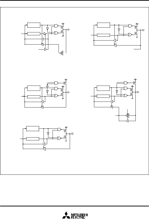
PRELIMINARY |
|||||||
|
|
|
|
|
|
. . |
|
|
|
|
|
|
specification |
change |
|
|
|
|
|
|
|
to |
|
|
|
|
a |
final |
|
subject |
|
|
is |
not |
are |
|
|
||
|
|
|
|
||||
|
limits |
|
|
|
|||
This |
|
|
|
|
|||
|
|
|
|
|
|||
|
|
|
|
|
|
|
|
Notice:parametric |
|
|
|
|
|
||
Some |
|
|
|
|
|
|
|
MITSUBISHI MICROCOMPUTERS
7534 Group
SINGLE-CHIP 8-BIT CMOS MICROCOMPUTER
(6) Port P14
|
Direction |
|
register |
Data bus |
Port latch |
Pulse output mode 
Timer output
CNTR0 interrupt input


(7) Ports P20 – P27 |
|
|
Direction |
|
register |
Data bus |
Port latch |
A-D conversion input 


Analog input pin selection bit
(8) Ports P30 – P35
Pull-up control |
|
Direction |
|
register |
Data bus |
Port latch |
(10) Ports P15, P16, P40, P41
|
Direction |
|
register |
Data bus |
Port latch |
(9) Port P36, P37
Pull-up control
|
Direction |
|
register |
Data bus |
Port latch |
INT interrupt input
P37/INT0 input level selection bit
*
*: P10, P12, P13, P36, P37 input levels are switched to the CMOS/TTL level by the port P1P3 control register. When the TTL level is selected, there is no hysteresis characteristics.
Fig. 15 Block diagram of ports (2)
15

PRELIMINARY |
|||||||
|
|
|
|
|
|
. . |
|
|
|
|
|
|
specification |
change |
|
|
|
|
|
|
|
to |
|
|
|
|
a |
final |
|
subject |
|
|
is |
not |
are |
|
|
||
|
|
|
|
||||
|
limits |
|
|
|
|||
This |
|
|
|
|
|||
|
|
|
|
|
|||
|
|
|
|
|
|
|
|
Notice:parametric |
|
|
|
|
|
||
Some |
|
|
|
|
|
|
|
MITSUBISHI MICROCOMPUTERS
7534 Group
SINGLE-CHIP 8-BIT CMOS MICROCOMPUTER
Interrupts
Interrupts occur by 14 different sources : 4 external sources, 9 internal sources and 1 software source.
Interrupt control
All interrupts except the BRK instruction interrupt have an interrupt request bit and an interrupt enable bit, and they are controlled by the interrupt disable flag. When the interrupt enable bit and the interrupt request bit are set to “1” and the interrupt disable flag is set to “0”, an interrupt is accepted.
The interrupt request bit can be cleared by program but not be set. The interrupt enable bit can be set and cleared by program.
It becomes usable by switching CNTR0 and A-D interrupt sources with bit 7 of the interrupt edge selection register, timer 2 and serial I/ O2 interrupt sources with bit 6, timer X and key-on wake-up interrupt sources with bit 5, and serial I/O transmit and INT1 interrupt sources with bit 4.
The reset and BRK instruction interrupt can never be disabled with any flag or bit. All interrupts except these are disabled when the interrupt disable flag is set.
When several interrupts occur at the same time, the interrupts are received according to priority.
Interrupt operation
Upon acceptance of an interrupt the following operations are automatically performed:
1.The processing being executed is stopped.
2.The contents of the program counter and processor status register are automatically pushed onto the stack.
3.The interrupt disable flag is set and the corresponding interrupt request bit is cleared.
4.Concurrently with the push operation, the interrupt destination address is read from the vector table into the program counter.
Notes on use
When the active edge of an external interrupt (INT0, INT1, CNTR0) is set, the interrupt request bit may be set.
Therefore, please take following sequence:
1.Disable the external interrupt which is selected.
2.Change the active edge in interrupt edge selection register. (in case of CNTR0: Timer X mode register)
3.Clear the set interrupt request bit to “0”.
4.Enable the external interrupt which is selected.
Table 6 Interrupt vector address and priority
|
Interrupt source |
Priority |
Vector addresses (Note 1) |
|
|
Interrupt request generating conditions |
|
|
|
|
|
|
|
|
|
|
Remarks |
||||||||||||||||||||||||||||||||||||||||||||||
|
|
|
|
|
|
|
|
|
|
|
|
|
|
|
|||||||||||||||||||||||||||||||||||||||||||||||||
High-order |
Low-order |
|
|
|
|
|
|
|
|
|
|
|
|
||||||||||||||||||||||||||||||||||||||||||||||||||
|
|
|
|
|
|
|
|
|
|
|
|
|
|
|
|
|
|
|
|
|
|
|
|
|
|
|
|
|
|
|
|
|
|
|
|
|
|
|
|
|
|
|
|
|
|
|
|
|
|
|
|
|
|
|
|
|
|
|
|
|
|
||
Reset (Note 2) |
1 |
FFFD16 |
FFFC16 |
At reset input |
|
|
|
Non-maskable |
|||||||||||||||||||||||||||||||||||||||||||||||||||||||
UART receive |
2 |
FFFB16 |
FFFA16 |
At completion of UART data receive |
|
|
|
Valid in UART mode |
|||||||||||||||||||||||||||||||||||||||||||||||||||||||
|
|
|
|
|
|
|
|
|
|
|
|
|
|
|
|
|
|
|
|
|
|
|
|
|
|
|
|
|
|
|
|
|
|
|
|
|
|
|
|
||||||||||||||||||||||||
USB IN token |
|
|
|
At detection of IN token |
|
|
|
Valid in USB mode |
|||||||||||||||||||||||||||||||||||||||||||||||||||||||
|
|
|
|
|
|
|
|
|
|
|
|
|
|
|
|
|
|
|
|
|
|
|
|
|
|
|
|
|
|
|
|
|
|
|
|
|
|
|
|
|
|
|
|
|
|
|
|
|
|
|
|
|
|
|
|
|
|
|
|
|
|
|
|
UART transmit |
3 |
FFF916 |
FFF816 |
At completion of UART transmit shift or |
|
|
|
Valid in UART mode |
|||||||||||||||||||||||||||||||||||||||||||||||||||||||
|
|
|
|
|
|
|
|
|
|
|
|
|
|
when transmit buffer is empty |
|
|
|
|
|
|
|
|
|
|
|
|
|
|
|
|
|
|
|
|
|
||||||||||||||||||||||||||||
|
|
|
|
|
|
|
|
|
|
|
|
|
|
|
|
|
|
|
|
|
|
|
|
|
|
|
|
|
|
|
|
|
|
|
|
|
|
|
|
|
|
|
|
|
|
|
|
|
|
|
|
|
|
|
|
|
|
|
|
|
|
|
|
USB SETUP/OUT token |
|
|
|
At detection of SETUP/OUT token or |
|
|
|
Valid in USB mode |
|||||||||||||||||||||||||||||||||||||||||||||||||||||||
Reset/Suspend/Resume |
|
|
|
At detection of Reset/ Suspend/ Resume |
|
|
|
|
|
|
|
|
|
|
|
|
|
|
|
|
|
|
|
|
|
||||||||||||||||||||||||||||||||||||||
|
|
|
|
|
|
|
|
|
|
|
|
|
|
|
|
|
|
|
|
|
|
|
|
|
|
|
|
|
|
|
|
|
|
|
|
|
|
|
|
|
|
|
|
|
|
|
|
|
|
|
|
|
|
|
|
|
|
|
|
|
|
|
|
INT1 |
|
|
|
At detection of either rising or falling edge |
|
|
|
External interrupt |
|||||||||||||||||||||||||||||||||||||||||||||||||||||||
|
|
|
|
|
|
|
|
|
|
|
|
|
|
of INT1 input |
|
|
|
(active edge selectable) |
|||||||||||||||||||||||||||||||||||||||||||||
|
|
|
|
|
|
|
|
|
|
|
|
|
|
|
|
|
|
|
|
|
|
|
|
|
|
|
|
|
|
|
|
|
|
|
|
|
|
|
|
||||||||||||||||||||||||
INT0 |
4 |
FFF716 |
FFF616 |
At detection of either rising or falling edge |
|
|
|
External interrupt |
|||||||||||||||||||||||||||||||||||||||||||||||||||||||
|
|
|
|
|
|
|
|
|
|
|
|
|
|
of INT0 input |
|
|
|
(active edge selectable) |
|||||||||||||||||||||||||||||||||||||||||||||
|
|
|
|
|
|
|
|
|
|
|
|
|
|
|
|
|
|
|
|
|
|
|
|
|
|
|
|
|
|
|
|
|
|
|
|
|
|
|
|
|
|
|
|
|
|
|
|
|
|
|
|
|
|
|
|
|
|||||||
Timer X |
5 |
FFF516 |
FFF416 |
At timer X underflow |
|
|
|
|
|
|
|
|
|
|
|
|
|
|
|
|
|
|
|
|
|
||||||||||||||||||||||||||||||||||||||
|
|
|
|
|
|
|
|
|
|
|
|
|
|
|
|
|
|
|
|
|
|
|
|
|
|
|
|
|
|
|
|
|
|
|
|
|
|
|
|
|
|
|
|
|
|
|
|
|
|
|
|
|
|
|
|
|
|
|
|
|
|
|
|
Key-on wake-up |
|
|
|
|
|
|
|
|
|
|
|
|
|
|
|
|
|
|
|
|
|
|
|
|
|
|
|
|
|
|
|
|
|
|
|
|
|
|
|
|
|
|
|
|
|
|
|
|
|
|
|
|
|
||||||||||
|
|
|
At falling of conjunction of input logical |
|
|
|
External interrupt (valid at falling) |
||||||||||||||||||||||||||||||||||||||||||||||||||||||||
|
|
|
|
|
|
|
|
|
|
|
|
|
|
level for port P0 (at input) |
|
|
|
|
|
|
|
|
|
|
|
|
|
|
|
|
|
|
|
|
|
||||||||||||||||||||||||||||
|
|
|
|
|
|
|
|
|
|
|
|
|
|
|
|
|
|
|
|
|
|
|
|
|
|
|
|
|
|
|
|
|
|
|
|
|
|
|
|
||||||||||||||||||||||||
Timer 1 |
6 |
FFF316 |
FFF216 |
At timer 1 underflow |
|
|
|
STP release timer underflow |
|||||||||||||||||||||||||||||||||||||||||||||||||||||||
Timer 2 |
7 |
FFF116 |
FFF016 |
At timer 2 underflow |
|
|
|
|
|
|
|
|
|
|
|
|
|
|
|
|
|
|
|
|
|
||||||||||||||||||||||||||||||||||||||
|
|
|
|
|
|
|
|
|
|
|
|
|
|
|
|
|
|
|
|
|
|
|
|
|
|
|
|
|
|
|
|
|
|
|
|
|
|
|
|
|
|
|
|
|
|
|
|
|
|
|
|
|
|
|
|
|
|
|
|
|
|
|
|
Serial I/O2 |
|
|
|
At completion of transmit/receive shift |
|
|
|
|
|
|
|
|
|
|
|
|
|
|
|
|
|
|
|
|
|
||||||||||||||||||||||||||||||||||||||
|
|
|
|
|
|
|
|
|
|
|
|
|
|
|
|
|
|
|
|
|
|
|
|
|
|
|
|
|
|
|
|
|
|
|
|
|
|
|
|
||||||||||||||||||||||||
CNTR0 |
8 |
FFEF16 |
FFEE16 |
At detection of either rising or falling edge |
|
|
|
External interrupt (active edge |
|||||||||||||||||||||||||||||||||||||||||||||||||||||||
|
|
|
|
|
|
|
|
|
|
|
|
|
|
of CNTR0 input |
|
|
|
selectable) |
|||||||||||||||||||||||||||||||||||||||||||||
|
|
|
|
|
|
|
|
|
|
|
|
|
|
|
|
|
|
|
|
|
|
|
|
|
|
|
|
|
|
|
|
|
|
|
|
|
|
|
|
|
|
|
|
|
|
|
|
|
|
|
|
|
|
|
|
|
|
|
|
|
|
|
|
A-D conversion |
|
|
|
At completion of A-D conversion |
|
|
|
|
|
|
|
|
|
|
|
|
|
|
|
|
|
|
|
|
|
||||||||||||||||||||||||||||||||||||||
|
|
|
|
|
|
|
|
|
|
|
|
|
|
|
|
|
|
|
|
|
|
|
|
|
|
|
|
|
|
|
|
|
|
|
|
|
|
|
|
|
|
|
|
|
|
|
|||||||||||||||||
BRK instruction |
9 |
FFED16 |
FFEC16 |
At BRK instruction execution |
|
|
|
Non-maskable software interrupt |
|||||||||||||||||||||||||||||||||||||||||||||||||||||||
|
|
|
|
|
|
|
|
|
|
|
|
|
|
|
|
|
|
|
|
|
|||||||||||||||||||||||||||||||||||||||||||
Note 1: Vector addressed contain internal jump destination addresses.
2: Reset function in the same way as an interrupt with the highest priority.
16
Loading...