


KDV-MP-5032
Table of contents
 Loading...
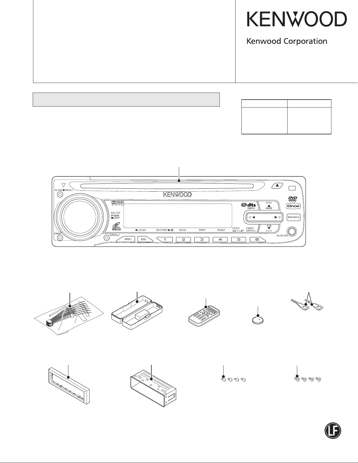
This product uses Lead Free solder.
This product complies with the
RoHS directive for the European market.
© 2008-5 PRINTED IN JA PAN
B53-0651-00
(
N
)
429
SERVICE MANUAL
KDV-3241Y/MP4339
/MP4439/MP5032
DVD RECEIVER
Illustrations is KDV-MP4339
KDV-MP4339
Panel assy
(A64-4707-08): KDV-MP4339
(A64-4708-08): KDV-MP4439
(A64-4709-08): KDV-3241Y
(A64-4710-08): KDV-MP5032
MODEL TDF PANEL No.
KDV-MP4339 A64-4703-08
KDV-MP4439 A64-4704-08
KDV-3241Y A64-4705-08
KDV-MP5032 A64-4706-08
DC cord assy
(E30-6855-08)
Panel escutcheon
(B01-0950-08)
Mounting hardware assy
(J22-0795-08)
Remote controller assy
without battery
(A70-2094-08)
Lever
(D10-7048-08) x2
Screw
(N09-6756-08)
x4
Screw
(N09-6757-08) x4
RC-DV460
Plastic cabinet
(A02-2758-08)
TDF SPARE-PANEL
Lithium battery
(Not supplied)
Mechanical parts in the DVD mechanism are not supplied.
2
KDV-3241Y/MP4339
/MP4439/MP5032
BLOCK DIAGRAM
FRONT BOARD
DVD/CD MECHA BOARD
SEE DVD BOARD BLOCK DIAGRAM
MAIN BOARD
MPX/ST DECODER
TUNER
AM & FM IF/PLL/
RDS OPTION
PROGRAM
E2PROM
AUTO ALIGMENT
TU101
DEMODULATOR
RDS
TUNER PACK
IC601
E-VOL
RSE OPTION
IC201
OPTION
AUX LINE MUTE
DOWN
FLIPDETA-
S/W S/W
CHABLE
CN503
KEY LIGHTING BL
5mA PER NODE
LCD B/LIGHTING
B
5mA PER NODE
DRIVER
LCD
IC901
NEGATIVE
LCD 14SEG
LCD1
BU302
KEY BLOCK
VOLUME
IR RECEIVER
VIDEO OUT
FRONT AUX IN &
CN902
CN901
CN502
RMC1
EV901
DVD DRIV IC 8V
DVD DVN CORE 1.2V
DVD LOADING MOTOR DRV IC 8V
DVD DIGITAL IC 3.3V
DVD PU 5V
LCD8.4V
POWER5V
LED8.4V
OP AMP
IC401
14 SEG
RDS DATA
RDS CLK
VCC +5V
RDS QUAL
SDA
SCL
SDA
SCL
AM AF/MPX
VCC +5V
TUNER 8.4V
POWER 5V
MAIN CLK
1187.5kHz
TUNER RDS
TUNER E2PROM
960kHz
MAIN CLK
TUNER INPUT
DVD/CD INPUT
AUX INPUT
SELECT
MAIN
REAR
SELECT
IN4
IN3
IN2
IN1
LOUDNESS
SOFT MUTE
VOLUME
TREBLE
MIDOLE
BASE
HPF
SUBWOOFER
15dB
R
L
SPECTRUM
ANALYZER
SACLKSAOUT
I2CBUS
SDACLK SMUTE
FAD
E
15dB
R
L
ACOUTRACOUTL
TUNER PART
4
55
56
65
68
71
70
69
67
72
83
29
AGND
CVBS
VGND
AUDIOL
DGND
PGND
23
84
85
86
CD/DVD PART
AUDIOR
SPDIF
1.2VD
5VPU
3.3VD
5V
8V
54
9
1
6
2
E-VR PART
RAM
FLASH E2PROM
FLMOD
REGC
RESET
SYSTEM CONTROL
VSS
EVDD
VDD
CMOS I/O : 86
CMOS OUTPUT : 1
N-ch 0.0 I/O : 4
TOTAL : 71
I/O PORT
AD CONVERTER
SERIAL INTERFACE
16BIT/8BIT/WATCH
TIMER
OPERATION
1.8V to 5.5V
78KO CPU
M
C
S
W
88
81/90
93/82
89
DLOAD PORT
CE2(TUNER)
SD/ST IND
CE1
DATA IN
RDS CLK
DATA OUT
CLK
RDS DATA
AF MUTE
QUALITY OUT
S-METER
SCLK
SOFT MUTE
SDA
SA OUT
SA IN(CLK)
MRESET
SPI TXD
SPI RXD
SPI CLK
SPI CE
RESET
DLOAD CLK
DLOAD DATA
FLMOD
VOLTAGE
61 AUDIO MUTE
50 AUX MUTE
DVD SPI CLK
480kHz
MAIN
X402X401
95
94
91
92
73
FRT-DET
5
GND
1
AUX L I
N
4
3
VIDEO
O
AUX R I
N
5 RMC
40 VOL DOWN
41
52
VOL UP
KEY 1
53 KEY 2 79 LCD CE
75
78
77
76
LCD RST
LCD CLK
LCD DATAI
LCD DATAO LED8.4V
LCD8.4V
PWR5V
BUZZER 80BEEP ON
SPDIF OUT
FLAT CABLE
MAIN u-COM
SYSTEM 5V
FCI 19PIN CONNECTOR(MALE)
FCI 19PIN CONNECTOR(FEMALE)
LCD CLK
MAIN
2.4MHz
LCD DR IC
3
2
1
3
KDV-3241Y/MP4339
/MP4439/MP5032
LINE MUTE
Q705-710
IC702
OP AMP CONTROL
MUTE
IC703
OP AMP
R/R
R/L
SW
SW
Q701-704
IC801
ISO
A.ANT
IC302
ZD302
ZD301
D301
D302
Q306
Q305
HAND-BRAKE
OPTION
IC501
CN403
JK501
DIGITAL
OUT
OPTION
VIDEO OUT
1Vp-p
5Vp-p
SPDIF OUT
CN801
Q308
Q301
Q302
IN
DIMMER
BATT CHECK
D305
D306
MULTI REGULATORIC301
DIODE
OPTION
D401-409
LOW
VOLTAGE
IC402
IC304IC305IC306
IC307
IC303
Q321
Q319
ZD304
Q322
CONTROL
FAN CONTROL
CN402
Q401
Q402
HTING BLK
R NODE
IGHTING BLK
R NODE
UT
UX IN &
JK703
ACC IN
ZD303
ZD306
TEL MUTE
IC403
VIDEO MUTE
FRONT LED/BACK LIGHTING
LINE/OUT
4V
FAN
E
E
HPF
SUBWOOFER
FADER
FADER
FADER
SMUTE
FADER
FADER
FADER
ACINL ACINR
OUTFL
OUTFR
OUTSW
OUTRL
OUTRR
MIXER
MIXER
AC GND
MUTE
SVR
11 9
25
8
3
5
2
4
12
22
10
HSD
2314
1
15
TAB
17
19
21
18
PW GND
24
S GND
13
16
ST BY
620
VCC1 VCC2
7
F/L
OUT FL-
OUT FL+
OUT FR+
OUT FR-
F/R
R/ROUT RR+
OUT RR-
OUT RL-
OUT RL+ R/L
A/ANT
REMOTE
T/MUTE
DIMMER
GND
HAND-BRAKE
BACK/UP
ACC
VCC
CTL
VOUT
N.C
C
GND
POWER ON
BACK UP(B+)
TER
ERFACE
ATCH
MAIN CLOCK : 8MHz
CLOCK
SUB CLOCK : 32.768kHz
WDT CLOCK : 240kHz
PORT
45
46
ART CHECK
44
ESET
LOAD CLK
LOAD DATA I/O
LMOD
ENABLE IN
UART IN
UART OUT
ANT ON63
59 DIMMER OUT
58 BLIGHT ON
66 DIMMER IN
38 ACC IN
16 MUTE
62 TEL MUTE
14 PWR ON
39 ACC OUT
87 ON
17 CONTROL
64 ON
61 AUDIO MUTE
MUTE3
10 ST BY
LINE OUT MUTE48
BAT CHK
42
REMOTE
HAND BRAKE DET
13
+
+
3.3V
PULL UP
VREF
14
12 7
410
6
2
3
VREF
CTL4
CTL3
CTL2
CTL1
BIAS TSD
VOLT
SENSE OVER
REAR
M2
S1
S2
M1
X402
94
91
92
OUT
CONT
IN
GND
43
1
2
1
4
2
OUT
CONT
IN
GND
3
CONT
2
OUT
4
IN
1
GND
3
2
CONT
4
GND
1
OUT
IN
3
POWER ON
V OUT
2
3
V IN
ADJ/GND
1
FAN 7.5V
POWER 5V(PULL UP,FRONT)
MAIN u-COM STANDBY 5V
TUNER VOL IC 8.4V
DVD DRIV IC 5V
DVD DVN CORE 1.2V
DVD DIGITAL IC 3.3VD
DVD LOADING MOTOR DRV IC 8V
DVD PU 5V
ILL 8.4V
FAN 7.5V
GND
AUX L IN
VIDEO OUT
AUX R IN
POWER
FAN
REMOTE
DVD/CD
VIDEO
AUTO
15/
81
RESET
REMOTE
ILL 8.4V
DRV IC 8V
STANDBY 5V
VOL IC 8.4V
MOTOR
DVD
TUNER
MAIN u-COM
BACK/UP
32-37
VOL IC 8.4V
BACK/UP
VB
CTL2
CTL3
CTL4
+
BLOCK DIAGRAM
4
KDV-3241Y/MP4339
/MP4439/MP5032
BLOCK DIAGRAM
Q1102
Q1101
CONTROL
LP
IC1201
DRIVER IC
MOTOR
STEPPING
SLED
BLDC
MOTOR
SPINDLE
DC MOTOR
LOADING
CN1203
CN1202
CN1201
DRIVER IC
IC1202
CN1301
MECH SWITCH
PICKUP UNIT
32MBIT
FLASH ROM
IC1502
SDRAM
IC1501
128MBIT
SERIAL E2PROM
8kBIT
IC1503
DVN
Q1401
MODULE
INTERFACE
CN1601
IC1402
MUTE
IC1401
AUDIO
DAC
FILTER
IC1603
VIDEO
6dB
X-TAL
27MHz
X1301
CLOCK
SYSTEM
REG
IC1601
REG
IC1602
CN1101
IC1301
AMP
VCC
HFM
RF
CD/DVD SW
A,B,C,D
E,F
CD-LD
DVD-LD
LPC
TRACK ACT
FOCUS ACT
LPCO1,LPCO2
LPC1,2
HFMDRV
RF,A,B,C,D,E,F
CD/DVD SW
MOS
POWER
MOS
POWER
MOS
POWER
ABS
POWER
MOS
ABS
ABSLOGIC
BRIDGE
3-PH
AMP
HALL
MATRIX
FODRV
TRDRV
SIN2
SIN1
FG
SPDRV
PHASE-B
PHASE-A
H1,H2,H3
A1,A2,A3
MOT-
MOT+ LMC1
LMC2
INNER SW
LDIN SW
DISC OUT SW
DISC IN SW
DISC IN
STBY
SERVO
APC FE
5V PU
5V
3.3VD
1.2VD
3.3VA
WE
OE
CE
BA1
WE
BA0RAS
CS
CAS
8V
8.4VA
5V
3.3VD
1.2VD
5V PU
SPI TX,SPI RX,SPI CE,SPI CLK
SPI SPI
R
LADOUT3
MD,MD,ML
DACCK,SRLK,BCK
DMUTE
A/V INTERFACE
BLOCK
AUDIO
VIDEO
BLOCK
3.3VD
5VA
8.4VA
RESET IN
VIDEO OUT
RESET
MEMORY INTERFACE
3.3V
8V
DISC IN
8.4VA
5V PU
5VA
3.3VA
A0-A17
D0-D15
MCLK
A0-A11
D0-D15
SCL
SDA
3.3VD 3.3VD 3.3VD
CONTROL
I2S
SPDIF
DAC4OUT
DISC IN
ZERO MUTE
RESET
CVBS
SPDIF
AUDIO L
AUDIO R
8.4VA
6dB
+
5
KDV-3241Y/MP4339
/MP4439/MP5032
TROUBLESHOOTING
1. System Control Error Correction Flow Chart
YES
YES
NO
Inside of CN802, F801
NO
CN801(16, 15)
NO
IC301(15, 14)
NO
IC401(100, 99, 81, 30, 50, 47, 97, 20, 51)
NO
NO
IC402, IC401(90)
X401, X402
NO
F301, Q301, Q302, IC401(38), CN801(14)
NO
CN901(19), IC401(74)
NO
CN901(14), IC401(21), Q316, Q317
NO
IC401(52, 53)
No power?
YES
Checked the Fuse?
YES
Checked the Back up Vdd and Gnd, Acc?
YES
Checked the Main Micom Back up Vdd?
YES
Checked the Main Micom Back up Gnd?
YES
Checked the Main Micom Reset?
YES
Checked the Main Micom X-tal?
YES
Checked the ACC in?
Checked the detachable switch?
YES
Checked the Front Panel VDD?
YES
Checked the Front Panel KEY input?
YES
OK
Something wrong with the system control?
YES
YES
NO
RMC1, R905
NO
CN901(5), IC401(5)
YES
Checked the Remocon Sens Vdd?
YES
Checked the Remocon Sens line?
OK
Something wrong with the system control?
Not available to Remocon?
YES
YES
NO
EV901, CN901(6, 7), IC401(40, 41)
NO
IC401(1, 2), IC601(22, 23)
YES
Checked the Encoder Volume?
YES
Checked the Volume IC control?
OK
Something wrong with the system control?
Not available to Volume control?
YES
YES
NO
SW901 ~ SW917, EV901
NO
CN901(8, 9), IC401(52, 53)
YES
Checked the Tact switch?
YES
Checked the Key line?
OK
Something wrong with the system control?
Not available to Key Control?
YES
YES
NO
CN801(5), Q305, Q306, IC401(62)
NO
IC401(1, 2, 3, 6, 61), IC601(21, 22, 23),
IC801(22), Q706, Q707, Q709, Q710
YES
Checked the tel mute input?
YES
Checked the Mute Control?
OK
Something wrong with the system control?
Not available to Telephone Mute?
YES
YES
NO
CN801(10), IC302, IC401(63)
Checked the ANT control?
YES
OK
Something wrong with the system control?
Not available to ANT(Motor Type) Control?
YES
YES
NO
CN801(6), IC301(12), IC401(87)
Checked the Remote control?
YES
OK
Something wrong with the system control?
Not available to Remote(Power AMP) control?
YES
YES
NO
IC601(24)
No sounds of All Functions?
YES
Checked the E-VR Vdd?
NO
IC601(15)
YES
Checked the E-VR Ground?
NO
IC601(22, 23), IC401(1, 2)
YES
Checked the E-VR control?
NO
IC601(21), IC401(6)
YES
Checked the E-VR Mute Control?
NO
IC601(5, 6, 7, 8, 11, 13, 16, 17, 18, 19, 20)
YES
Checked the E-VR Signal in/out?
NO
IC801(6, 20)
YES
Checked the Power IC Vdd?
NO
IC801(1, 2, 8, 13, 18, 24)
YES
Checked the Power IC Ground?
NO
IC801(4, 22), IC401(3, 10)
YES
Checked the Power IC Control?
NO
IC801(3, 5, 7, 9, 11, 12, 14, 15, 17, 19, 21, 23)
YES
Checked the Power IC Signal in/out?
NO
CN801(1, 2, 3, 4, 8, 9, 12, 13)
YES
Checked the main connector?
OK
Something wrong With the Sound?
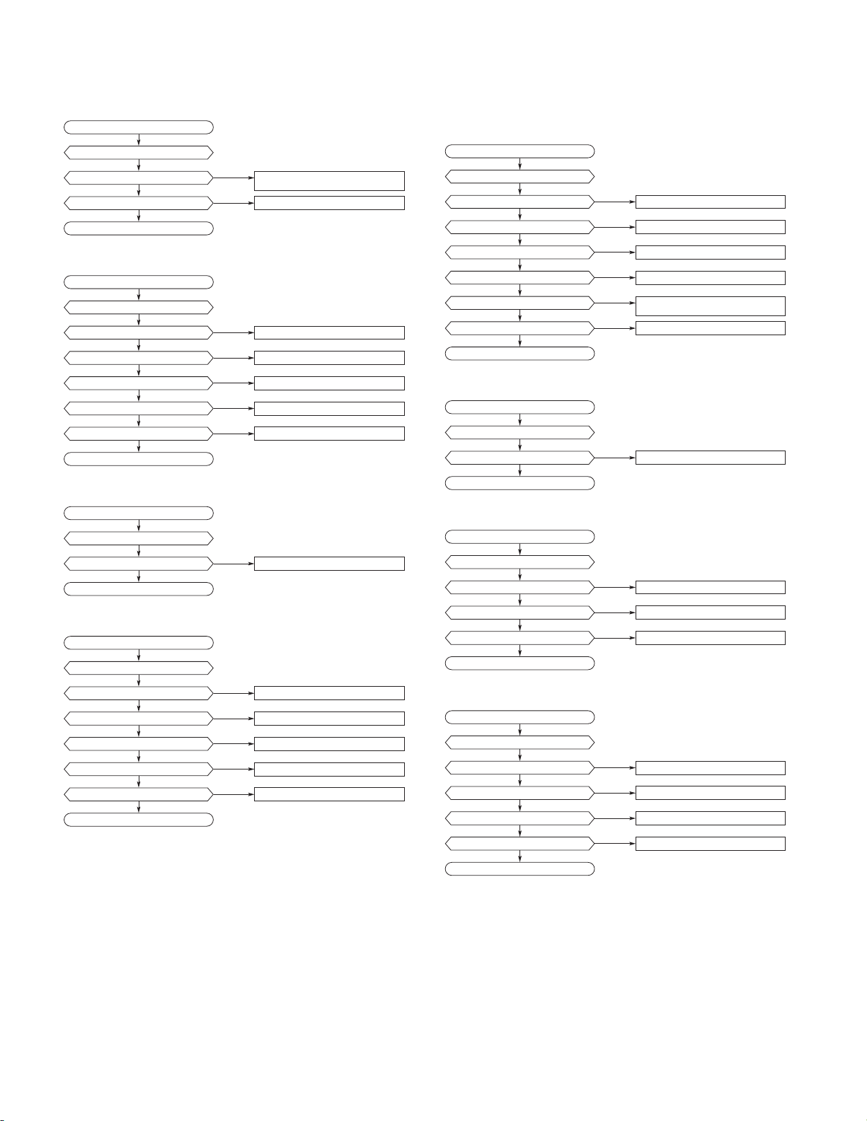
2. Sound Error Correction Flow Chart
6
KDV-3241Y/MP4339
/MP4439/MP5032
YES
YES
NO
IC401(1, 2, 3, 6, 61), IC601(21, 22, 23),
IC801(22), Q706, Q707, Q709, Q710
YES
Checked the Mute Control?
NO
TU101(19), IC401(4)
YES
Checked the AF mute?
OK
Something wrong With the Sound?
Hearing the Pop Noise?
YES
YES
NO
Q308, F303, IC701(8)
YES
Checked the Line Out AMP Vdd?
NO
Q309, IC401(64)
YES
Checked the Line Out AMP Vdd control?
YES
NO
IC701(4)
Checked the Line Out AMP Ground?
YES
NO
IC401(48), Q705, Q701, Q703
Checked the Line Out AMP Mute Contorl?
YES
NO
IC701(1, 2, 3, 5, 6, 7)
Checked the Line Out AMP Signal in/out?
OK
Something wrong With the Sound?
No REAR Line out signal?
YES
YES
NO
IC401(80), BU302
YES
Checked the Beep Control?
OK
Something wrong With the Sound?
No output Beep sound?
YES
YES
NO
Q308, F303, IC702(8)
YES
Checked the Line Out AMP Vdd?
NO
Q309, IC401(64)
YES
Checked the Line Out AMP Vdd control?
YES
NO
IC702(4)
Checked the Line Out AMP Ground?
YES
NO
IC401(48), Q705, Q701, Q703
Checked the Line Out AMP Mute Contorl?
YES
NO
IC702(1, 2, 3, 5, 6, 7)
Checked the Line Out AMP Signal in/out?
OK
Something wrong With the Sound?
No Subwoofer Line out signal?
YES
YES
NO
IC901(56)
YES
Checked the LCD Driver Vdd?
NO
IC901(59)
YES
Checked the LCD Driver Ground?
NO
IC901(61), CN901(11), IC401(75)
NO
IC901(60)
NO
IC401(76, 78, 79), CN901(3, 4, 10),
IC901(62, 63, 64)
NO
IC901(1 ~ 55), LCD
Checked the LCD Driver RESET?
YES
Checked the LCD Driver OSC?
YES
Checked the LCD Driver data interface?
YES
Checked the LCD to LCD Driver line?
YES
OK
Something wrong with the Display?
No Display or Some Display is broken?
YES
YES
NO
IC601(25, 26), IC401(9, 54)
YES
Checked the Level Meter Signal Input?
OK
Something wrong with the Display?
Don't moved Level dancing bar?
YES
YES
NO
F302, CN801(11), IC401(66), IC301(9)
YES
Checked the Dimmer control input?
NO
IC301(4), CN901(13)
YES
Checked the LED Vdd?
NO
LD901 ~ LD919, LD922 ~ LD926
Checked the LED?
YES
OK
Something wrong with the Display?
Not available to illumination with button?
YES
YES
NO
F302, CN801(11), IC401(66), IC301(9)
YES
Checked the Dimmer control input?
NO
IC301(4), Q320, Q322, CN901(12)
YES
Checked the LCD Vdd?
NO
IC401(58, 59), Q319, Q321
NO
LD920 ~ LD921
Checked the LCD Vdd control?
Checked the LED?
YES
YES
OK
Something wrong with the Display?
Not avaliable to LCD Lighting control?
3. Display Error Correction Flow Chart
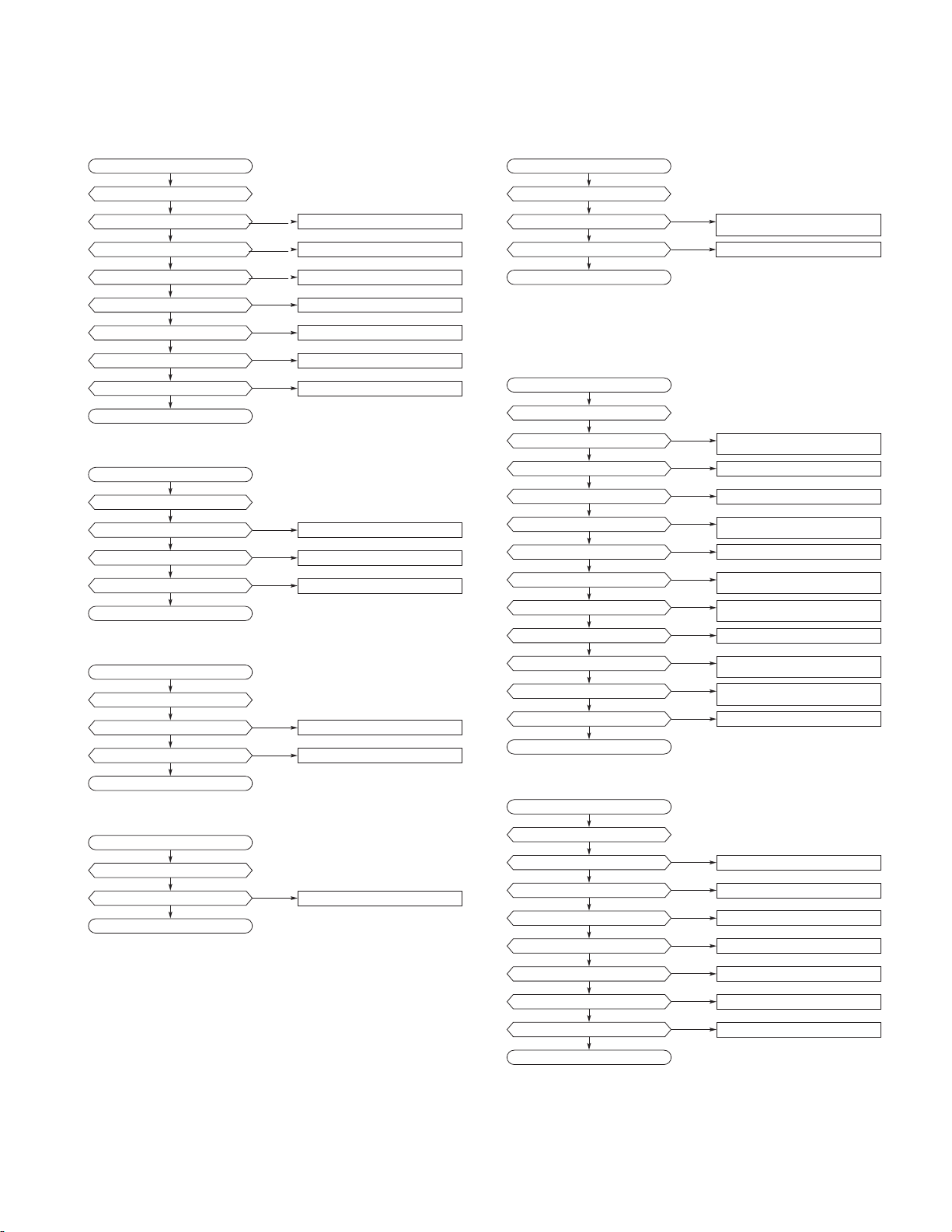
TROUBLESHOOTING
7
KDV-3241Y/MP4339
/MP4439/MP5032
YES
YES
NO
TU101(6, 17), Q307, IC301(10, 14)
YES
Checked the Tuner Vdd?
NO
IC401(39, 64), Q318, IC301(11)
YES
Checked the Tuner Vdd control?
NO
TU101(3, 7, 12, 16)
NO
TU101(14, 15), IC401(1, 2)
NO
TU101(1, 2)
NO
TU101(8), IC401(4)
NO
TU101(5), IC401(67)
Checked the Tuner Ground?
YES
Checked the I2C data?
YES
Checked the RF signal in?
YES
Checked the Mute Control?
Checked the SD level(RDS model)?
YES
YES
OK
Something wrong With the Tuner system?
Not available to Tuner?
YES
YES
NO
TU101(10, 11), IC601(5, 6)
YES
Checked the Tuner Signal out?
NO
TU101(8), IC401(4)
YES
Checked the mute?
NO
See the Sound Error correction Process.
Checked the E-VR & Power AMP?
YES
OK
Something wrong With the Tuner system?
Tuner no sound?
YES
YES
NO
TU101(4), IC401(55)
YES
Checked the S-METER level?
NO
TU101(19, 20), IC401(65, 83)
YES
Checked the RDS data?
OK
Something wrong With the Tuner system?
Not available to AF?
YES
YES
NO
TU101(19, 20), IC401(65, 83)
YES
Checked the RDS data?
OK
Something wrong With the Tuner system?
Not available to RDS function?
YES
YES
NO
JK901, CN910, CN503, CN901(15, 17),
IC601(11, 13)
YES
Checked the AUX Signal input?
NO
See the Sound Error correction Process.
YES
Checked the E-VR & Power AMP?
OK
Something wrong With the Tuner system?
AUX no sound?
YES
YES
NO
See the System error correction
Process with the key control.
YES
Checked the Eject Key defect?
NO
IC1202(1, 6)
NO
IC1202(7, 8, 2, 3). See Fig.9.
NO
CN1301(2, 4), SW1301, CN1202(13).
See Fig.9~12.
NO
IC1301(VDD33, VDD12, +3VA). See Fig.13.
NO
IC1301 VSS (1, 23, 35, 46, 63, 81, 100,
171, 180, 198, 208, 220, 245)
NO
IC401(23), IC203(5, 6) CN902(10),
IC1301 NRST(101), CN1601 M_RESET(10)
NO
X1301(1, 3). See Fig.14.
NO
IC401(84, 85, 86, 29), CN902(4, 5, 6, 7)
IC1301(84, 85, 86, 87)
NO
CN902(4, 5, 6, 7) CN1601(4, 5, 6, 7).
See Fig.15.
NO
CN1301(2, 4)
Checked the Loading Motor IC Vdd?
YES
Checked the Load/Unload Control?
YES
Checked the Load/Unload SW?
YES
Checked the MPEG VDD?
YES
Checked the MPEG Ground?
YES
Checked the MPEG Reset?
YES
Checked the MPEG X-tal?
YES
Checked the Main Micom Data Interface?
YES
Checked the Main Micom Data Interface?
YES
Checked the Disc in load switch?
YES
OK
Something wrong With the DVD system?
No Loading/Unloading?
YES
YES
NO
IC1301(161)
YES
Checked the MPEG Video Signal out?
NO
IC1603(3, 5). See Fig.30.
Check the 6dB Amplifier Vcc, GND?
YES
NO
IC1603(2, 4). See Fig.30.
Check the 6dB Amplifider In, Out?
YES
NO
IC403(6, 7, 8). See Fig.31.
Check the IC403’s Vcc & GND?
YES
NO
IC403(3, 4, 5). See Fig.31, 32.
Check the IC403’s IN, Out, Mute Signal?
YES
NO
TM1(1, 2)
Check the Brake Line?
YES
NO
CN403(1, 2)
Check the RCA Cable?
OK
YES
Something wrong With the DVD system?
Can hear the sound but not display on monitor?
4. Tuner Error Correction Flow Chart 5. AUX Error Correction Flow Chart
6. DVD Error Correction Flow Chart
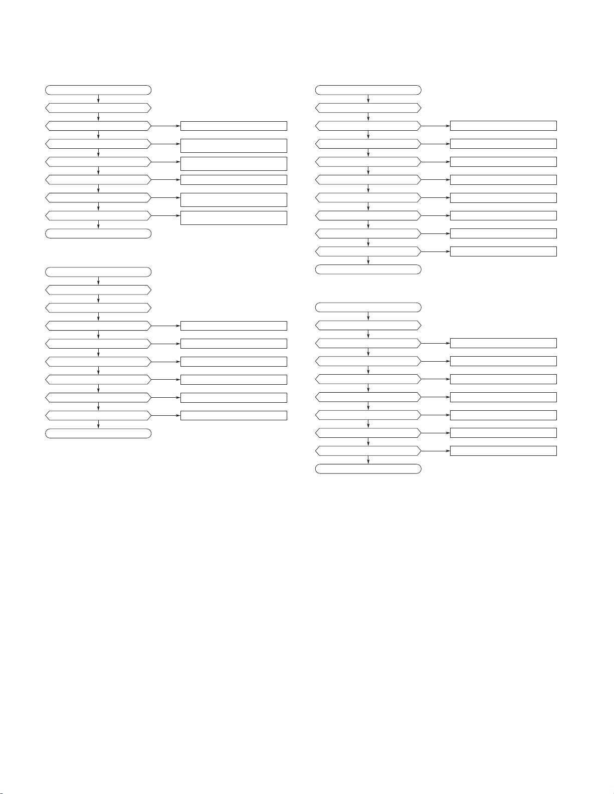
TROUBLESHOOTING
8
KDV-3241Y/MP4339
/MP4439/MP5032
YES
YES
NO
IC1301(VDD33,VDD12,+3VA). See Fig.13.
YES
Checked the Input voltage of MPEG IC?
NO
IC1301 VSS (1, 23, 35, 46, 63, 81, 100,
171, 180, 198, 208, 220, 245)
Checked the GND Condition of MPEG IC?
YES
NO
IC401(23), IC203(5, 6) CN902(10), IC1301
NRST(101), CN1601 M_RESET(10)
Checked the MPEG RESET?
YES
NO
X1301(1, 3). See Fig.14.
Check the MPEG X-tal?
YES
NO
IC401(84, 85, 86, 29), CN902(4, 5, 6, 7)
IC1301(84, 85, 86, 87)
Checked the Main Micom Data Interface?
YES
NO
CN902(4, 5, 6, 7), CN1601(4, 5, 6, 7).
See Fig.15.
Checked the Main Micom Data Interface?
YES
OK
Something wrong With the DVD system?
Front LCD : “INIT” Display?
YES
YES
YES
No Spindle Motor Operating?
NO
IC1201(22, 27, 43)
Checked the Spindle Driver IC Vdd?
YES
NO
IC1201(4, 16)
Checked the Spindle Driver IC VHALF?
YES
NO
IC1201(36, 38, 41)
Checked the Spindle Driver IC GND?
YES
NO
IC1201(37, 39, 40). See Fig.16.
Checked the A1, A2, A3 of The Driver IC?
YES
NO
IC1201(27~33). See Fig.17.
NO
IC1201(5). See Fig.17.
Checked the Hall Bias Signals?
Checked the spindle motor control?
YES
YES
OK
Something wrong With the DVD system?
No Reading & “FILE CHECK” DISPLAY?
YES
YES
YES
Checked the Limit SW?
NO
IC1201(18). See Fig.19.
NO
CN1202(13), IC1301(75). See Fig.18.
Checked the Motor DRV mute control?
YES
NO
IC1201(10). See Fig.20.Checked the focus control?
YES
NO
FMON0. See Fig.20.
Checked the focus error level out.(FE Mon)?
YES
NO
IC1201(9). See Fig.21.
Checked the tracking control?
YES
NO
FMON1. See Fig.21.
NO
IC1301(117). See Fig.22.
NO
IC1201(6, 7). See Fig.23, 24.
Checked the Tracking error level out.(TE Mon)?
Checked the RF signal out check?
Checked the sled motor control?
YES
YES
YES
OK
Something wrong With the DVD system?
No Reading & “FILE CHECK” DISPLAY?
YES
YES
YES
Checked the MPEG Audio DATA out?
NO
IC1401(4, 5, 6, 9, 10). See Fig.25.
NO
IC1301(172, 173, 174,175)
Checked the DAC Vcc,Vdd, GND?
YES
NO
IC1401(1, 2, 3, 7, 8, 16). See Fig.26, 27.
Checked the DAC signal In/out?
YES
NO
IC1301(178), IC1401(11, 12). See Fig.28.
Checked the DAC Mute?
YES
NO
IC1402(4, 8). See Fig.29.
Checked the OP AMP VDD, GND?
YES
NO
IC1402(1, 2, 6, 7). See Fig.29.
NO
See a Sound Error correction Process.
Checked the OP AMP Signal in/out?
Checked the E-VR & Power AMP?
YES
YES
OK
Something wrong With the DVD system?
DVD/CD no sound?
TROUBLESHOOTING
9
KDV-3241Y/MP4339
/MP4439/MP5032
●
MAIN MICROCOMPUTER: EAN36171501 (MAIN UNIT IC401)
Pin No Pin Name I/O Description
1 PPLL_SCL O Clock output for interface with PLL IC & EEPROM (TU101 15pin)
2 PPLL_DO O Data for PLL IC & EEPROM (TU101 14pin)
3 PPWR_MUTE O Power AMP. Direct Mute Control Output (IC801 27pin)
4 PAF_MUTE O For TUNER AF Mute (TU101 8pin)
5 PRMC I Remote controller input
6 PSOFT_MUTE O Volume I.C Direct volume mute signal output (IC601 15pin)
7 N.C. O Not to be used
8 N.C. O Not to be used
9 PEV_SACLK O Volume I.C Spectrum Analyzer Clock output (IC601 16pin)
10 PSTANDBY O Power AMP. Standby Control Output (IC801 27pin)
11 N.C. O Not to be used
12 PDVD_PICKUP_PWR O DVD Vdd Control. 1. DVD Pickup 5V control output. 2. DVD Motor 8V control output
13 PHAND_BREAK I Hand Break signal input. Active : High Level.
14 PDVD_POWER O DVD system Vdd control output (IC304 4pin)
15 N.C. O Not to be used
16 PVIDEO_R_MUTE O Rear Video Signal mute control output
17 PFAN O Fan control output (Q402)
18,19 N.C. O Not to be used
20 EVss1 Connect to GND
21 PFRT_PWR O Front 5V control output (Q313). Power control output for front panel
22 N.C. O Not to be used
23 PDVD_RST O DVD MPEG reset control (IC203 5pin)
24 PZERO_MUTE I DVD/CD zero mute signal input
25~28 N.C. O Not to be used
29 PDVD_CE O DVD MPEG CE control (IC203 2pin)
30 EVdd1 I Positive power supply (+5V)
31 PDVD33 O DVD MPEG 3.3V Vdd on/off control output (Q304)
32 POPT_IN0 I For diode option check, signal 1 or 2 input 0 (See Tuner band option)
33 POPT_IN1 I For diode option check, signal 1 or 2 input 1 (See Tuner band option)
34 POPT_IN2 I For diode option check, signal 1 or 2 input 2 (See Tuner band option)
35 POPT_OUT0 O For diode option check, signal 1 output (See Tuner band option)
36 POPT_OUT1 O For diode option check, signal 2 output (See Tuner band option)
37 POPT_OUT2 O For diode option check, signal 3 output (See Tuner band option)
38 PACC I ACC Control Input (Q301)
39 PAUDIO_PWR O Regulator Audio (Tuner and E-VR) 8.4V ON Control Output (IC301 11pin)
40 PVOLA I Volume rotary encoder A terminal signal input
41 PVOLB I Volume rotary encoder B terminal signal input
42 PBAT_CHK I Backup level detect input
43 N.C. I Not to be used
44 N.C. O Not to be used
MICROCOMPUTER’S TERMINAL DESCRIPTION
10
KDV-3241Y/MP4339
/MP4439/MP5032
Pin No Pin Name I/O Description
45 PEV_DO O To volume controller, data output (IC601 12pin)
46 PEV_CLK O Clock for interface with volume controller (IC601 13pin)
47 Avref I Reference voltage applied to A/D converter
48 PLINE_MUTE O LINE-OUT MUTE ON/OFF Control (Q705)
49 N.C. O Not to be used
50 Avref0 I Reference voltage applied to D/A converter
51 Avss - GND
52 PKEY1 I Key 1st line signal input
53 PKEY2 I Key 2nd line signal input
54 PLVL_METER I Volume I.C Spectrum Analyzer Analog Level Input (IC601 26pin)
55 PS_MTR I Radio station's strength signal input (TU101 4pin)
56 PQUALTY I Radio station's strength signal input (TU101 9pin)
57 N.C. O Not to be used
58 PLIGHT O Front LCD back light On/Off Control Output (Q319)
59 PDIMMER O Dimmer Control output for LCD back light
60 PAUX_MUTE O Not to be used
61 PAUDIO_MUTE O System Audio Mute Control Output (Q706). Active : HIGH Level.
62 PTEL_MUTE I Tuner Signal Out Mute Control (Q305). Active : Low Level.
63 PANT O Antenna control output (IC302 1pin). Active : HIGH Level.
64 PPWR O
Power on control. 1. Line out B+ on/off control (Q309)
2. Illumination On/off control (IC301 9Pin). 3. Tuner 5V control control (Q318)
65 PRDS_DI I From tuner pack, RDS data input (TU101 19Pin)
66 PDIM_IN I Dimmer input
67 PSSTOP O TUNER seek stop signal out (TU101 5Pin)
68 PRDS_RST O RDS decoder reset control ouput (TU101 18Pin)
69 N.C. I Not to be used
70 PART_EN I ART Enable input, only Auto test equipment
71 PART_RX I Data input for ART, only Auto test equipment
72 PART_TX O Data output for ART, only Auto test equipment
73 N.C. O Not to be used
74 PFRT_DETECT I Front Panel detaching or attaching detect
75 PFRT_RST O Front LCD driver reset
76 PFRT_DO O Data output to Front LCD driver
77 PDISC_IN I Wake up signal input from DVD Mecha with Disc in
78 PFRT_CLK O CLK output to Front LCD driver
79 PFRT_CE O Data enable output to Front LCD driver
80 PBEEP O Buzzer output
81 PEXLVI I Low voltage detector (Connect to Vdd)
82 N.C. I Not to be used
83 PRDS_CLK I From tuner pack, RDS clock input (TU101 20Pin)
84 PDVD_DO O Data output for DVD
MICROCOMPUTER’S TERMINAL DESCRIPTION
11
KDV-3241Y/MP4339
/MP4439/MP5032
Pin No Pin Name I/O Description
85 PDVD_DI I Data input of DVD
86 PDVD_CLK O CLK output of DVD
87 PREMOTE O External amp on (IC301 13Pin)
88 Download_CLK - CLK for Program upgrade
89 Download_IO - Data I/O for fl ash memory programmer (Pull-up register)
90 RESET - System reset input
91 SUB CLK I Sub clock 32.768 kHz
92 SUB CLK O Sub clock 32.768 kHz
93 FLMOD - Flash memory programming mode setting
94 MAIN CLK I X’tal 19.2 MHz
95 MAIN CLK O X’tal 19.2 MHz
96 REGC - Connect to VSS via a capacitor.
97 Vss - Ground
98 Evss - Ground Potential for Ports
99 Vdd I Positive power supply (+5V)
100 Evdd I Positive power supply (+5V) For Ports
TUNER BAND OPTION
D401 D402 D403 AREA STEP
X X X OIRT 50K/9K
X O X LATINE/R 100K/10K
O X X ASIA/M/X 100K/9K
O O X EUROPE/E2 50K/9K
X X O EUROPE(LW)
X O O USA
D404 O RDS SEEK PI
D405 O Not Used
D406 O RDS ON
D407 O Not Used
MICROCOMPUTER’S TERMINAL DESCRIPTION
12
KDV-3241Y/MP4339
/MP4439/MP5032
CIRCUIT DESCRIPTION
INTERNAL BLOCK DIAGRAM OF IC’S
OIPMG78431A (MAIN UNIT IC301)
• PIN FUNCTION (Note1)
Pin No. Pin name Function
Protection function
Normal
operation
TSD On
(Note2)
VB=24V
(Note3)
VB=50V
(Note3)
1 GND Ground - - - -
2 FREG_B External Trs bass drive (Note4) On/Off On/Off Off Off
3 FREG_F FREG feedback terminal On/Off On/Off Off Off
4 ILMOUT 8.4V output for JLM/500mAmax On/Off Off Off Off
5 CTL4 FREG control terminal - - - -
6 CDOUT 8.0V output for CD/1.3Amax (Note4) On/Off Off Off Off
7 DSPOUT 3.3V output for DSP/250mAmax (Note4) On/Off Off Off Off
8 VB Battery - - - -
9 CTL3 ILM control terminal - - - -
10 AUDIOOUT 8.4V output for AUDIO/500mAmax (Note4) On/Off Off Off Off
11 CTL1 DSP, CD, Audio control terminal - - - -
12 EXTOUT High side output/600mAmax (Note4) On/Off Off Off Off
13 CTL2 EXT control terminal - - - -
14 VDDOUT 5.7V output for micro controller (Note4) On On On Off
15 VBUP Back up - - - -
GND
BIAS
VB
+B
VDDOUT
AUDIOOUT
ILMOUT
CTL 1
GND
TAB
V
REF
1.5V
Over voltage detect
TSD
V
REF
CDOUT
V
REF
EXTOUT
VBUP
DSPOUT
CTL 2
2.5V
CTL 3
2.5V
CTL 4
2.5V
15
FREG F
RFREG3
FREG B
13
12
11
10
9
8
7
6
5
4
3
2
1
14
3.5V
DBUP
CBUP
100uF
CVDD
10uF
CDSP
10uF
CAUDIO
10uF
CCD
0.1uF
CEXT
10uF
CILM
0.1uF
CFREG
10uF
QFREG
RFREG1
RFREG2
DEXT1
DEXT2
C1
100uF
C2
0.1uF
• BLOCK DIAGRAM
Note1.
In the uper table. “On” means always On. “Off” means
compulsory Off and “On/Off” means that it can con-
trol by control terminal.
Note2.
Thermal protection circuit
A built-in thermal protection circuit (TSD:Thermal shut
down) prevents thermal damage to the IC. All outputs
except VDD (pin14) and FREG (pin2&3) are switched
off when the circuit operates, revert to the original
state when the temperature drops to a certain level.
Note3.
Overvoltage protection circuit
The overvoltage protection circuit (surge protector)
turns off all outputs without Vdd, when VB voltage
is more than about 21V. And the overvoltage protec-
tion circuit (surge protector) turns off Vdd output with
other all outputs, when VB voltage is more than about
26V. When the overvoltage protection operates on
VB>=18V condition, the stand by current increases.
Note 4.
Overcurrent protection circuit
FREG_B (pin2), ILMOUT (pin4), CDOUT (pin6),
DSPOUT (pin7), AUDIOOUT (pin10), EXITOUT (pin12),
VDDOUT (pin14) output circuits are built-in overcur-
rent protection circuit based on the respective output
current. These overcurrent protection circuits limit
the current with a curve shape of “7” in the voltage-
current graph. This prevents IC destruction due to
overcurrent.
13
KDV-3241Y/MP4339
/MP4439/MP5032
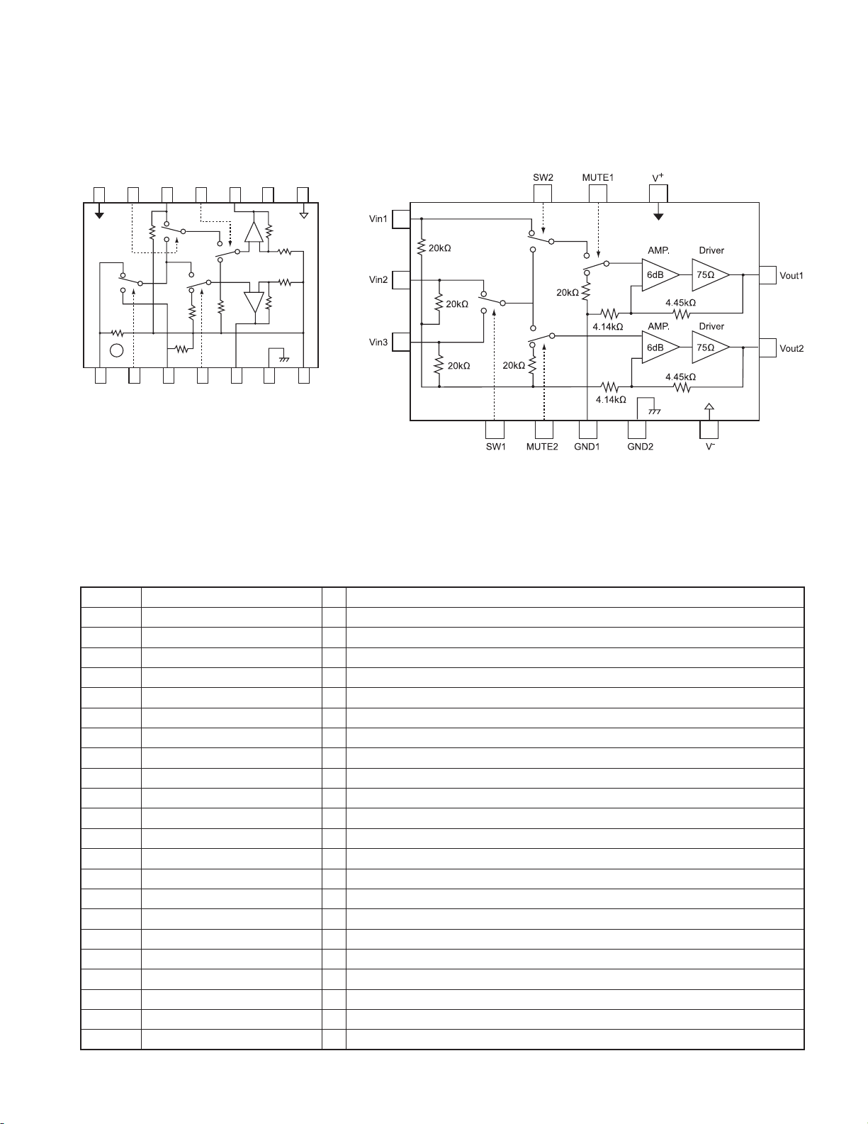
OIPRPJR004A (MAIN UNIT IC403)
• PIN CONFIGURATION • BLOCK DIAGRAM
14 13 12 11 10
1
2
98
123456
7
PIN FUNCTION
1. Vin3
2. SW1
3. Vin2
4. MUTE2
5. Vout2
6. GND2
7. GND1
8. V
+
9. N. C.
10. Vout1
11. MUTE1
12. Vin1
13. SW2
14. V
-
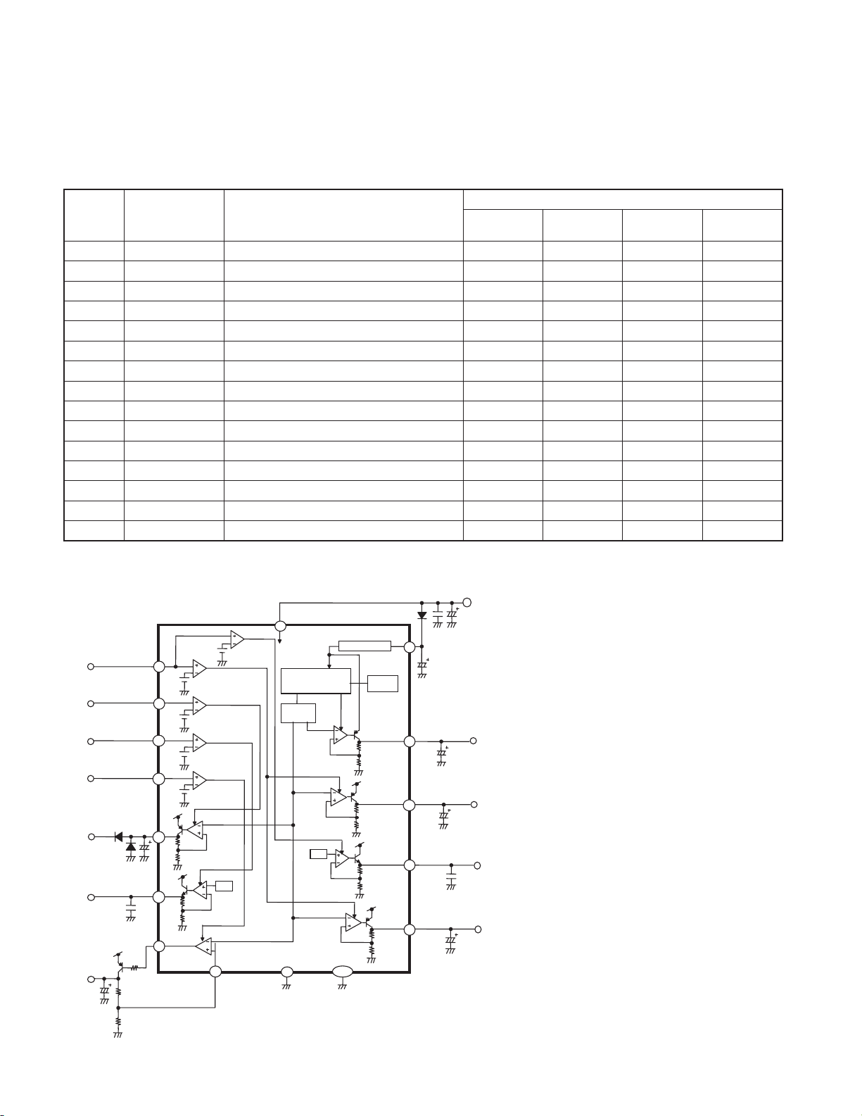
E-TDA7419 (MAIN UNIT IC601)
• PIN DESCRIPTION
Pin No. Pin Name I/O Function
1 ACOUTR / AC2OUTR O AC coupling right output / HPF fi lter AC2OUT right channel
2 ACINR / FILOR I/O AC coupling right input / HPF fi lter FILO right channel
3 ACINL / FILOL I/O AC coupling left input / HPF fi lter FILO left channel
4 ACOUTL / AC2OUTL O AC coupling left output / HPF fi lter AC2OUT left channel
5 SE3L / ACINL I Single-ended input 3 left channel / AC coupling left input
6 SE3R / ACINR I Single-ended input 3 right channel / AC coupling right input
7 SE2L I Single-ended input 2 left channel
8 SE2R I Single-ended input 2 right channel
9 SE1L I Single-ended input 1 left channel
10 SE1R I Single-ended input 1 Right channel
11 DIFFL I Pseudo differential stereo input left
12 DIFFG I Pseudo differential stereo input common
13 DIFFR I Pseudo differential stereo input right
14 CREF O Reference capacitor
15 GND S Ground
16 OUTSW / OUTLR2 O Subwoofer output / 2nd rear left output
17 OUTRF O Front right output
18 OUTRR O Rear right output
19 OUTLR O Rear left output
20 OUTLF O Front left output
21 MUTE I External mute pin
22 SCL I I2C bus clock
CIRCUIT DESCRIPTION
14
KDV-3241Y/MP4339
/MP4439/MP5032
OUTL F
OUTRF
OUTLR
OUTRR
INPUT
MULTIPLEXE
R
InGain
AutoZero
I
2
C BUSDIGITAL CONTROL
OUTSW/
OUTLR2
MUTE
Loudness MiddleTreble BassSoftMute
Softstep
Volume
Softstep
MonoFader
Softstep
MonoFader
Softstep
MonoFader
SUPPLY
VDD CREFGND
SDASCL
DIFFG
DIFFL
SE1R
SE1L
DIFFR
SE2L
SE2R
Spectrum
Analyzer
Softstep
MonoFader
Subwoofer
LPF
Mix
Mix
MIX/
OUTSW/
OU
TRR2
HPF
HPF
Softstep
MonoFader
Softstep
MonoFader
AC2INL/
SE3L
AC2INR/
SE3R
ACOUTL/
AC2OUTL
ACOUTR/
AC2OUTR
ACINL/
FILOL
ACINR/
FILOR
VREFOUTF
SAOU T SACL K
InGain
OUTL F
OUTRF
OUTLR
OUTRR
INPUT
MULTIPLEXER
InGain
AutoZero
I
2
C BUSDIGITAL CONTROL I
2
C BUSDIGITAL CONTROL
OUTSW/
OUTLR2
MUTE
Loudness MiddleTreble BassSoftMute
Softstep
Volume
Softstep
MonoFader
Softstep
MonoFader
Softstep
MonoFader
SUPPLY
VDD CREFGND
SDASCL
DIFFG
DIFFL
SE1R
SE1L
DIFFR
SE2L
SE2R
Spectrum
Analyzer
Softstep
MonoFader
Subwoofer
LPF
Mix
Mix
MIX/
OUTSW/
OU
TRR2
HPF
HPF
Softstep
MonoFader
Softstep
MonoFader
AC2INL/
SE3L
AC2INR/
SE3R
ACOUTL/
AC2OUTL
ACOUTR/
AC2OUTR
ACINL/
FILOL
ACINR/
FILOR
VREFOUTF
SAOU T SACL K
InGain
Pin No. Pin Name I/O Function
23 SDA I/O I2C bus data
24 VDD S Supply
25 SAIN I Spectrum analyzer clock input
26 SAOUT O Spectrum analyzer output
27 VREF O Vref output
28 MIX / OUTSW / OUTRR2 I/O Mix input / Additional subwoofer output / 2nd rear right output
• BLOCK DIAGRAM
CIRCUIT DESCRIPTION
Loading...