


 Loading...
KENWOOD KDC-W4031, KDC-W4031Y, KDC-W409, KDC-W409Y, KDC-W431GY Service Manual
...
CD RECEIVER
KDC-W4031/Y
KDC-W409/Y
KDC-W431GY
KDC-W4531/Y
KDC-WF431A
SERVICE MANUAL
© 2004-12 PRINTED IN JAPAN B53-0230-00 (N) 1813
PANEL ASSY |
PANEL ASSY |
KDC-W4031/Y (A64-3455-02) |
KDC-W409/Y (A64-3456-02) |
VOL |
|
|
|
|
|
VOL |
|
|
|
|
|
AUD |
|
|
|
|
/PTY |
AUD |
|
|
|
|
/PTY |
SET UP |
|
|
|
|
SET UP |
|
|
|
|
||
MENU |
FF |
SCAN |
RDM |
REP |
F.SEL |
MENU |
FF |
SCAN |
RDM |
REP |
F.SEL |
PANEL ASSY |
|
|
|
|
PANEL ASSY |
|
|
|
KDC-W431GY (A64-3457-02) |
|
|
KDC-W4531/Y |
(A64-3454-02) |
|
|||
|
|
|
|
|
|
|
|
External Media Control |
VOL |
|
|
|
|
|
VOL |
|
|
AUD |
|
|
|
|
|
AUD |
|
/PTY |
SET UP |
|
|
|
|
|
SET UP |
|
|
MENU |
FF |
SCAN |
RDM |
REP |
F.SEL |
MENU FF |
SCAN RDM REP |
F.SEL M.RDM |
PANEL ASSY |
|
|
|
|
|
|
|
|
KDC-WF431A (A64-3466-02) |
|
|
SPARE TDF PANEL |
|
|
|||
|
|
|
|
|
|
|
|
|
|
|
|
|
|
|
MAIN UNIT NAME |
TDF PARTS No. |
TDF NAME |
|
|
|
|
|
|
KDC-W4031/Y |
Y33-2140-60 |
TDF-W4531 |
|
|
|
|
|
|
KDC-W409/Y |
Y33-2140-65 |
TDF-W409 |
AUD |
|
|
|
|
|
KDC-W431GY |
Y33-2140-61 |
TDF-W431GY |
VOL |
|
|
|
|
|
|
|
|
SET UP |
|
|
|
|
|
/PIY |
Y33-2140-60 |
TDF-W4531 |
MENU |
FF |
SCAN |
RDM |
REP |
F.SEL |
KDC-W4531/Y |
||
|
|
|
|
|
|
KDC-WF431A |
Y33-2140-63 |
TDF-WF431 |
LEVER |
DC CORD |
PLASTIC CABINET ASSY |
MOUNTING HARDWARE ASSY |
(D10-4589-04) x2 |
(E30-6413-05) |
(A02-2736-03) |
(J21-9716-03) |
ANTENNA ADAPTOR |
* ESCUTCHEON |
(T90-0523-05) |
(B07-xxxx-xx) |
* Depends on the model. Refer to the parts list.
This product uses Lead Free solder.
KDC-W4031/W4031Y/W409/W409Y
KDC-W431GY/W4531/W4531Y/WF431A
|
|
|
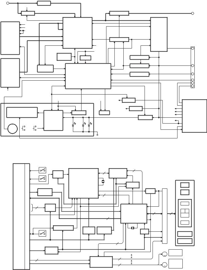
BLOCK DIAGRAM |
|
|
|
|
J4 |
L506 |
|
ELECTRIC UNIT (X34-) |
|
|
|
|
FM AGC |
|
|
|
|
|
|
|
ANT |
|
|
|
|
|
|
|
|
AM+B |
|
|
|
|
|
|
|
Q501 |
|
|
Q351,352 |
J6 |
|
|
|
AM AGC |
|
|
PRE MUTE |
|
|
|
|
|
IC10 |
|
PRE OUT |
|||
|
|
|
IC4 |
FM (J/K Type) |
: 1800mV |
||
|
|
|
|
|
|||
|
|
|
|
|
FM (E Type) |
: 1372mV |
|
|
SERVO |
MPX OUT |
|
AM (J/K Type) |
: |
600mV |
|
CD or MD |
|
|
|
AM (E Type) |
: |
855mV |
|
A8V |
|
|
|
||||
MECHA |
MPX IN |
|
|
CD/MD RECEIVER : 3600mV |
|||
BU5V |
|
POWER IC |
|||||
|
|
|
CHANGER |
: 3600mV |
|||
AUDIO OUT |
800mV |
|
E-VOL |
IC6 |
|
|
|
1200mV |
|
& |
|
|
|
|
|
|
|
MUTE LOGIC |
|
|
|
||
|
|
TUNER |
|
|
|
||
|
|
|
|
|
|
|
|
|
|
|
A8V |
|
J1 |
|
|
|
IC11 |
|
|
|
|
SP OUT |
|
|
|
BU5V |
Q51 |
|
|
|
|
J2 |
E2PROM |
IC8 |
|
|
|
||
RST IC |
SURGE DET |
|
|
|
|||
|
|
|
|
|
|
||
CHANGER |
IC7 |
|
IC1 |
Q52 |
|
|
|
|
|
BU DET |
|
BACK-UP |
|||
|
RDS |
|
|
|
|||
|
|
|
Q53 |
|
|
|
|
AUDIO OUT |
DECODER |
|
|
|
|
|
|
|
|
|
ACC DET |
|
ACC |
|
|
|
|
|
|
|
|
||
|
|
|
SYSTEM u-COM |
|
|
TEL MUTE |
|
|
|
|
|
|
|
||
|
|
|
|
|
|
P-ANT |
|
|
|
|
|
|
|
P-CON |
|
BACK-UP |
|
|
|
|
|
|
|
|
|
|
|
|
|
|
|
|
|
|
IC3 |
|
|
|
|
|
|
|
|
|
|
|
|
|
Q151 |
|
|
|
|
|
|
|
|
|
|
PAN5V |
|
|
|
BU5V |
|
|
|
|
|
|
|
|
|
POWER SUPPLY IC |
|
SWITCH UNIT (X16-) |
|
|
|
|
PAN5 |
PAN5V |
|
|
|
|
|
||||||||
|
|
|
|
|
|
|
|
|
|
||||||||||
|
|
|
|
|
|
|
|
|
|
|
P-CON |
||||||||
ED1 |
|
|
|
|
|
|
|
|
|
|
|
|
Q72,73 |
|
|
|
|
|
|
|
|
|
|
|
|
|
|
|
|
|
|
|
|
|
|
|
P-ANT |
||
|
|
IC1 |
|
|
|
|
|
|
|
|
|
SERVO |
|
|
|
|
|||
|
|
|
|
|
IC3 |
|
|
Q155 |
SERVO |
|
|
SW5V |
SW5V |
||||||
VFD |
|
|
|
|
REMOTE |
|
DSI |
|
|
|
|
|
IC15 |
|
|
AM+B |
AM+B |
||
|
|
|
|
|
|
|
|
|
|
|
|
A8V |
AUDIO+B |
||||||
|
|
|
|
|
|
|
|
|
|
|
|
|
|
|
|
|
|||
|
|
|
VFD DRIVER |
|
|
|
|
|
|
|
|
|
|
|
|
|
|||
|
|
|
|
|
|
|
|
|
|
|
|
VFD REG |
|
|
|
VCC |
|||
S11 |
|
|
|
with |
KEY ILLUMI |
|
|
|
|
|
|
|
|
|
|
|
|
BU5V |
|
....... |
KEY MATRIX |
|
|
|
|
|
|
|
|
|
|
|
|
|
ILLUMI |
||||
|
|
|
|
....... |
|
|
|
|
|
|
|
|
|
|
|
|
BU5V |
||
|
|
|
|
|
|
|
|
|
|
|
|
|
|
|
|
|
|
|
|
VOL |
|
|
|
|
|
|
|
|
|
|
|
|
|
|
|
|
|
|
|
CD PLAYER UNIT (X32-5500-00) |
|
|
|
|
|
|
|
|
|
|
|
|
|
|
|
||||
CN1 |
|
|
|
|
|
|
|
|
|
|
|
|
|
|
|
|
|
|
|
DOUT |
24 |
OPEN |
|
|
IC1 |
|
|
|
IC3 |
|
|
|
|
|
|
|
|
|
|
|
|
S2 |
|
Q1,4 |
|
|
|
|
|
4 |
|
|
|
|
|
|
|||
12EJE |
23 |
|
|
|
|
8 |
|
MP3/WMA |
|
|
|
|
|
|
|||||
|
|
LEVEL |
|
|
|
|
|
|
|
|
|
|
|
||||||
|
|
|
|
|
|
|
|
|
|
|
|
|
|
|
|||||
|
|
|
|
|
|
|
|
|
DECODER |
|
|
|
|
|
DPU1 |
||||
|
|
S1 |
|
SHIFT |
|
|
|
|
16.00MHz |
|
|
|
|
|
|||||
|
|
|
|
|
|
|
|
|
|
|
|
|
|
|
|||||
DATA |
20 |
|
|
MICROPROCESSOR |
X2 |
|
|
|
BUFFER |
|
|
|
|
|
LD |
||||
LOS |
22 |
|
|
|
MECHANISM |
|
|
|
|
|
|
IC8 |
|
|
|
|
(OPTICAL PICKUP) |
||
CLK |
21 |
|
|
|
CONTROL |
|
|
|
|
|
|
|
|
|
|
|
|
|
|
|
|
IC9 |
|
|
|
|
|
|
|
|
|
|
|
Q9,10 |
CN2 |
|
|
||
A8V |
19 |
A8V |
DAC 3.3V |
A3.3V |
|
|
|
|
|
|
|
|
|
|
SW |
|
|
|
PD |
|
AVR |
|
|
|
|
1 |
|
|
|
|
|
|
|
|
|
|
|||
L |
18 |
|
|
|
|
|
|
|
|
|
|
|
|
|
|
|
|
||
|
|
|
|
|
|
|
|
|
|
|
|
|
|
|
|
|
|
||
AGND |
17 |
|
|
|
|
|
|
|
|
|
|
|
|
|
|
|
|
|
|
R |
16 |
|
Q3,5,6 |
|
|
BU3.3V |
|
|
|
IC2 |
|
|
|
|
|
|
|
||
|
|
|
|
|
|
|
|
|
|
|
|
|
|
E |
|||||
MUTER |
15 |
3 |
LEVEL |
|
|
|
|
|
|
|
|
|
|
|
|
|
|
||
|
|
|
|
|
|
|
|
|
|
|
|
|
|
|
|||||
MUTEL |
14 |
|
|
|
|
|
|
|
|
|
|
|
|
|
|
|
|||
|
SHIFT |
|
|
|
|
|
|
|
|
|
|
|
|
|
|
|
|||
MRST |
13 |
|
|
|
|
|
|
|
|
RF AMP/SERVO |
|
5 |
|
16 |
A B |
||||
|
|
|
|
|
|
|
|
|
|
|
|
||||||||
|
|
|
|
|
|
|
|
|
|
|
|
CD SIGNAL |
|
|
|
|
|||
MSTOP |
12 |
|
|
|
|
|
|
|
|
|
|
|
|
|
|
|
C |
||
|
|
|
|
|
|
|
3 |
|
|
PROCESSOR |
|
|
|
|
|||||
|
|
|
|
|
|
|
|
|
|
|
|
|
|
|
|
||||
|
|
|
|
LEVEL SHIFT |
BU 3.3V |
DAC 3.3V |
|
BU2.5V |
|
|
|
VREF |
|
|
|
F |
|||
|
|
|
|
Q7 |
|
IC6 |
|
IC7 |
|
|
|
|
X1 |
|
|
|
|
|
|
|
|
|
|
|
|
|
|
|
|
|
Q8 |
|
|
|
|
|
|||
|
|
|
|
|
|
|
|
|
|
|
|
|
|
|
|
|
|
|
|
LOE/LIM |
10 |
S3 |
|
|
|
AVR |
|
AVR |
|
|
|
|
16.898MHz |
APC |
|
|
TR COIL |
||
|
|
|
|
|
|
|
|
|
|
|
|
|
|
|
|
||||
BU5 |
9 |
BU5V |
|
|
|
|
|
|
|
|
|
|
|
|
|
|
|
|
|
|
|
|
|
|
|
|
|
|
4 |
|
|
|
|
|
|
FO COIL |
|||
DGND |
8 |
|
|
|
|
|
|
|
|
|
|
|
|
|
|
|
|||
|
IC5 |
|
|
|
|
|
|
|
|
|
|
|
|
|
|
|
|
||
DGND |
7 |
|
|
SW3.3V |
|
|
|
|
|
|
|
|
|
|
|
|
|
||
D5 |
6 |
D5V |
SW 3.3V |
|
|
|
|
|
|
|
|
|
|
DM1 SPINDLE |
|
||||
|
|
|
|
|
|
|
|
|
|
|
|
|
|||||||
D5 |
5 |
|
AVR |
|
PON |
|
|
|
|
|
|
|
|
|
|
|
|||
LO/EJ |
4 |
|
|
|
|
IC4 |
|
|
|
|
|
FCS |
|
|
|
M |
MOTOR |
|
|
|
|
|
|
|
|
|
|
4 |
|
|
|
|
|
||||||
|
|
2 |
|
|
|
|
|
|
|
|
|
TRK |
|
|
|
|
|
|
|
MOTOR |
3 |
|
|
|
|
4ch BTL |
|
|
|
SPD |
|
|
|
DM2 |
LOADING |
|
|||
|
|
S7V |
|
|
|
|
|
|
|
|
|
||||||||
S7V |
2 |
|
|
|
|
DRIVER |
|
4 |
|
SLD |
|
|
|
M |
& SLED |
|
|||
|
|
|
|
|
|
|
|
|
|
|
|||||||||
SGND |
1 |
|
|
|
|
|
|
|
|
|
|
|
|
|
|
|
MOTOR |
|
|
|
|
|
|
|
|
|
|
|
|
|
|
|
|
|
|
|
|||
|
|
|
|
|
|
|
|
|
|
|
|
|
|
|
|
|
|
||
2
KDC-W4031/W4031Y/W409/W409Y
KDC-W431GY/W4531/W4531Y/WF431A
COMPONENTS DESCRIPTION
● ELECTRIC UNIT (X34-3402-7x)
Ref. No. |
Application / Function |
Operation / Condition |
|
|
|
IC1 |
SYSTEM -COM |
System control. |
|
|
|
IC3 |
POWER SUPPLY |
DC5Vx2, 7.9Vx1, 8.1Vx1, 10.3V, P.CON, P-ANT output. |
|
|
|
IC4 |
POWER IC |
Audio signal amplifier. |
|
|
|
IC6 |
MUTE LOGIC |
Mute control. |
|
|
|
IC7 |
RDS DECODER |
RDS decode. |
|
|
|
IC8 |
RESET |
“L” when detection voltage goes below 3.6V. |
|
|
|
IC10 |
E-VOL & TUNER |
E-VOL, Tuner, Stereo decode. |
|
|
|
IC11 |
E2PROM |
Saves and writes tuner adjustment data. |
|
|
|
IC15 |
VFD REGULATOR |
11.3V output voltage for LED and VFD. |
|
|
|
Q51 |
SERGE DET |
“ON” when the base goes “H”. |
|
|
|
Q52 |
BU DET |
“ON” when the base goes “H”. |
|
|
|
Q53 |
ACC DET |
“ON” when the base goes “H”. |
|
|
|
Q71 |
SERVO+B CONTROL SW |
“ON” when the base goes “H”. |
|
|
|
Q72,73 |
SERVO+B AVR |
Output voltage level : 7.5V. |
|
|
|
Q74 |
IC3 CONTROL SW |
“ON” when the base goes “H” (Output voltage : 10.3V). |
|
|
|
Q151 |
PANEL 5V SW |
“ON” when the base goes “L”. |
|
|
|
Q155 |
DSI ILLUMI SW |
“ON” when the base goes “L”. |
|
|
|
Q252 |
IC4 STBY SW |
“ON” when the base goes “L”. |
|
|
|
Q330 |
Q351, 352 MUTE DRIVER |
“ON” when the base goes “L”. |
|
|
|
Q351 |
Lch PRE MUTE SW |
Pre-output is muted when the base goes “H”. |
|
|
|
Q352 |
Rch PRE MUTE SW |
Pre-output is muted when the base goes “H”. |
|
|
|
Q501 |
AM RF AMP |
Adjusts for AM-RF gain. |
|
|
|
● CD PLAYER UNIT (X32-5500-00)
Ref. No. |
Application / Function |
Operation / Condition |
|
|
|
|
|
|
|
Focusing, tracking, sled and spindle servo processing. |
|
IC1 |
MECHANISM CONTROL |
Automatic adjustment (Focusing, tracking, gain, offset and balance) operations. |
|
MICROPROCESSOR |
Digital signal processing (DSP, PLL, sub-codes, CIRC error correction, audio data |
||
|
|||
|
|
interpolation) operations, and microcomputer function. |
|
|
|
|
|
|
|
Generation of RF signal based on the signals from the APC circuit and pickup, and |
|
IC2 |
RF AMP/SERVO CD |
generation of servo error (Focusing error and tracking error) signals. |
|
SIGNAL PROCESSOR |
Detection of dropout, anti-shock, track crossing and off-track conditions, included |
||
|
|||
|
|
gain control function during CD-RW. |
|
|
|
|
|
IC3 |
MP3/WMA DECODER |
|
|
|
|
|
|
IC4 |
4ch BTL DRIVER |
Focusing coil, tracking coil, spindle motor and sled motor driver, disc loading and |
|
eject operation. |
|||
|
|
||
|
|
|
|
IC5 |
SW 3.3V AVR |
|
|
|
|
|
|
IC6 |
BU 3.3V AVR |
3.3V power supply for back-up. |
|
|
|
|
|
IC7 |
BU 2.5V AVR |
2.5V power supply for back-up. |
|
|
|
|
3
KDC-W4031/W4031Y/W409/W409Y
KDC-W431GY/W4531/W4531Y/WF431A
COMPONENTS DESCRIPTION
Ref. No. |
Application / Function |
Operation / Condition |
|
|
|
IC8 |
SELECTOR (SERIAL DATA) |
Serial audio data switch. |
|
|
|
IC9 |
DAC 3.3V AVR |
3.3V power supply for IC2. |
|
|
|
Q1 |
LEVEL SHIFT |
3.3V to 5.0V. |
|
|
|
Q3~7 |
LEVEL SHIFT |
3.3V to 5.0V. |
|
|
|
Q8 |
AUTOMATIC POWER CONTROL |
LD driver. |
|
|
|
Q9,10 |
SWITCH |
Switch for anticipation sub-beam delay. |
|
|
|
● SWITCH UNIT (X16-2932-7x)
Ref. No. |
Application / Function |
Operation / Condition |
|
|
|
IC1 |
VFD DRIVER |
|
|
|
|
IC3 |
REMOTE SENSOR |
|
|
|
|
Q1 |
GREEN LED SW |
“ON” when the base goes “H”. |
|
|
|
Q2 |
RED LED SW |
“ON” when the base goes “H”. |
|
|
|
Q21 |
PAN SW5V |
“ON” when the base goes “H”. |
|
|
|
MICROCOMPUTER’S TERMINAL DESCRIPTION
● SYSTEM -COM : IC1 on X34- (ELECTRIC UNIT)
Pin No. |
Active |
Pin Name |
I/O |
Application |
Processing Operation |
|
(H/L) |
||||||
|
|
|
|
|
||
|
|
|
|
|
|
|
1 |
|
DC ERR |
I |
DC offset detection input |
|
|
|
|
|
|
|
|
|
2 |
|
LINE MUTE |
I |
Phone detection |
NAVI MUTE : Over 2.5V, TEL MUTE : Below 1V |
|
|
|
|
|
|
|
|
3 |
|
ROTARY CW |
I |
Rotary encoder input |
|
|
|
|
|
|
|
|
|
4 |
|
AVSS |
- |
|
|
|
|
|
|
|
|
|
|
5 |
|
TUN TYPE1 |
I |
E-VOL setting switch |
Refer to “TUN TYPE” on the TRUTH TABLE |
|
|
|
|
|
|
|
|
6 |
|
TUN TYPE2 |
I |
E-VOL setting switch |
Refer to “TUN TYPE” on the TRUTH TABLE |
|
|
|
|
|
|
|
|
7 |
|
AVREF1 |
- |
|
|
|
|
|
|
|
|
|
|
8 |
|
VFD DATAF |
I |
Data input from VFD driver |
|
|
|
|
|
|
|
|
|
9 |
|
VFD DATAS |
O |
Data output to VFD driver |
|
|
|
|
|
|
|
|
|
10 |
|
VFD CLK |
O |
Clock output to VFD driver |
|
|
|
|
|
|
|
|
4
KDC-W4031/W4031Y/W409/W409Y KDC-W431GY/W4531/W4531Y/WF431A
MICROCOMPUTER’S TERMINAL DESCRIPTION
Pin No. |
Active |
Pin Name |
I/O |
Application |
Processing Operation |
|
(H/L) |
||||||
|
|
|
|
|
||
|
|
|
|
|
|
|
11 |
L |
VFD RST |
O |
Reset output to VFD driver |
Display OFF, Key reset, TDF panel OFF : L |
|
Display ON, Key scan : H |
||||||
|
|
|
|
|
||
|
|
|
|
|
|
|
12 |
|
VFD CE |
O |
Chip enable output to VFD driver |
|
|
|
|
|
|
|
|
|
13 |
|
ROTARY CCW |
I |
Rotary encoder input |
|
|
|
|
|
|
|
|
|
14 |
L |
TDF DET |
I |
TDF panel detection |
TDF panel OFF : H, TDF panel ON : L |
|
|
|
|
|
|
|
|
15 |
|
PWIC BEEP |
O |
Beep output |
|
|
|
|
|
|
|
|
|
16 |
|
LX DATA S |
I |
Data from slave unit |
|
|
|
|
|
|
|
|
|
17 |
|
LX DATA M |
O |
Data to slave unit |
|
|
|
|
|
|
|
|
|
18 |
|
LX CLK |
I/O |
LX-BUS clock |
|
|
|
|
|
|
|
|
|
19 |
|
RDS AFSL |
O |
Tuner RDS mute output |
Refer to “RDS AFSL” on the TRUTH TABLE |
|
|
|
|
|
|
|
|
20 |
L |
TUN ADJ |
I |
For adjusting IC10 |
Adjustment=H, PS1-1,2=L, PS1-3=Hi-Z, |
|
PS2-1,2=Hi-Z, TUN DATA, CLK=Hi-Z |
||||||
|
|
|
|
|
||
|
|
|
|
|
|
|
21 |
|
TUN SD |
I |
Tuner search stop output |
H : Station exists, L : Station does not exist |
|
|
|
|
|
|
|
|
22 |
H |
LX RST |
O |
Hard reset to slave unit |
H : Reset, L : Normal condition |
|
|
|
|
|
|
|
|
23 |
H |
LX CON |
O |
Start-up request to slave unit |
H : Slave unit ON, L : Slave unit OFF |
|
|
|
|
|
|
|
|
24 |
|
LX REQ M |
O |
Communication request to slave unit |
|
|
|
|
|
|
|
|
|
25 |
|
AUD SDA |
I/O |
Volume + tuner I2C data input and output |
|
|
|
|
|
|
|
|
|
26 |
|
AUD SCL |
I/O |
Volume + tuner I2C clock input and output |
|
|
|
|
|
|
|
|
|
27 |
H |
PWIC STBY |
O |
Power IC standby output |
Power IC ON : H, Power IC OFF : L |
|
|
|
|
|
|
|
|
28 |
H |
VOL MUTE |
O |
E-VOL mute output |
L : Mute OFF, Hi-Z : Mute ON |
|
|
|
|
|
|
|
|
29 |
L |
PWIC MUTE |
O |
Power IC mute output |
Power OFF : L, Standby : L, Tel mute : L |
|
|
|
|
|
|
|
|
30 |
|
TUN FANC OUT |
O |
Tuner block (inside the -com) check |
OK : L, NG : H |
|
|
|
|
|
|
|
|
31 |
|
RESET2 |
O |
Mute for reset |
Output L |
|
|
|
|
|
|
|
|
32 |
|
RDS DATA |
I |
RDS decoder data input |
|
|
|
|
|
|
|
|
|
33 |
|
VSS1 |
- |
|
|
|
|
|
|
|
|
|
|
34 |
|
RDS QUAL |
I |
RDS decoder QUAL input |
|
|
|
|
|
|
|
|
|
35 |
L |
ACC DET |
I |
ACC detection |
ACC exists : L, ACC does not exist : H |
|
|
|
|
|
|
|
|
36 |
L |
BU DET |
I |
Momentary power-down detection |
BU exists : L |
|
BU does not exist (Momentary power-down) : H |
||||||
|
|
|
|
|
||
|
|
|
|
|
|
|
37 |
|
NC |
- |
|
|
|
|
|
|
|
|
|
|
38 |
|
PS2-2 |
O |
Power supply control output |
Refer to “POWER IC CONTROL” on the TRUTH TABLE |
|
|
|
|
|
|
|
|
39 |
|
PS2-1 |
O |
Power supply control output |
Refer to “POWER IC CONTROL” on the TRUTH TABLE |
|
|
|
|
|
|
|
|
40 |
|
PS1-1 |
O |
Power supply control output |
Refer to “POWER IC CONTROL” on the TRUTH TABLE |
|
|
|
|
|
|
|
|
41 |
|
PS1-2 |
O |
Power supply control output |
Refer to “POWER IC CONTROL” on the TRUTH TABLE |
|
|
|
|
|
|
|
|
42 |
|
PS1-3 |
O |
Power supply control output |
Refer to “POWER IC CONTROL” on the TRUTH TABLE |
|
|
|
|
|
|
|
|
43,44 |
|
NC |
- |
|
|
|
|
|
|
|
|
|
|
45 |
|
CD MUTE |
I |
CD mute request |
L : Mute request |
|
|
|
|
|
|
|
|
46 |
L |
CD MSTOP |
O |
CD mecha u-com stop |
H : mecha -com operates, L : mecha -com is stopped |
|
|
|
|
|
|
|
|
47 |
|
CD LOE LIM SW |
I |
CD detection (chucking switch) |
H : Loading is finished, L : Disc does not exist |
|
|
|
|
|
|
|
5
KDC-W4031/W4031Y/W409/W409Y KDC-W431GY/W4531/W4531Y/WF431A
MICROCOMPUTER’S TERMINAL DESCRIPTION
Pin No. |
Active |
Pin Name |
I/O |
Application |
Processing Operation |
|
(H/L) |
||||||
|
|
|
|
|
||
|
|
|
|
|
|
|
48 |
|
CD LOEJ |
I/O |
CD motor control |
Refer to “CD MECHA CONTROL OPERATION” |
|
|
on the TRUTH TABLE |
|||||
|
|
|
|
|
||
|
|
|
|
|
|
|
49 |
|
CD MOTOR |
O |
CD motor control |
Refer to “CD MECHA CONTROL OPERATION” |
|
|
on the TRUTH TABLE |
|||||
|
|
|
|
|
||
|
|
|
|
|
|
|
50 |
|
NC |
- |
|
|
|
|
|
|
|
|
|
|
51 |
L |
CD MRST |
O |
CD mecha -com reset |
H : Normal condition, L : Reset |
|
|
|
|
|
|
|
|
52 |
|
CD SCL |
I/O |
CD mecha I2C clock output |
|
|
|
|
|
|
|
|
|
53 |
|
CD DISC12 SW |
I |
12cm CD detection |
|
|
|
|
|
|
|
|
|
54 |
|
CD LOS SW |
I |
CD loading detection |
|
|
|
|
|
|
|
|
|
55 |
|
CD SDA |
I/O |
CD mecha I2C data input and output |
|
|
|
|
|
|
|
|
|
56 |
|
OEM DISP CE |
I/O |
External display chip enable |
External display |
|
|
|
|
|
|
|
|
57 |
|
OEM DISP CLK |
I/O |
External display clock |
External display |
|
|
|
|
|
|
|
|
58 |
|
OEM DISP DATA |
I/O |
External display chip data |
External display |
|
|
|
|
|
|
|
|
59 |
|
DSI |
O |
DSI control |
DSI ON : H, DSI OFF : L, TDF DET=H (DSI blinks) |
|
|
|
|
|
|
|
|
60 |
L |
RESET |
I |
|
|
|
|
|
|
|
|
|
|
61 |
|
NC |
- |
|
|
|
|
|
|
|
|
|
|
62 |
L |
PON FL |
O |
VFD power supply ON |
VFD ON : H, VFD OFF : L |
|
TDF DET H (DSI blinks) : L, TDF DET L : H |
||||||
|
|
|
|
|
||
|
|
|
|
|
|
|
63 |
|
KEY REQ |
I |
Communication request from VFD driver |
L : Key input |
|
|
|
|
|
|
|
|
64 |
|
RDS CLK |
I |
RDS decoder clock input |
|
|
|
|
|
|
|
|
|
65 |
|
REMOTE |
I |
Remote control input |
|
|
|
|
|
|
|
|
|
66 |
|
LX REQ S |
I |
Communication request from slave unit |
|
|
|
|
|
|
|
|
|
67 |
|
VSS0 |
- |
|
|
|
|
|
|
|
|
|
|
68 |
|
VDD1 |
- |
|
|
|
|
|
|
|
|
|
|
69 |
|
X2 |
- |
|
|
|
|
|
|
|
|
|
|
70 |
|
X1 |
- |
|
|
|
|
|
|
|
|
|
|
71 |
|
TEST |
- |
|
|
|
|
|
|
|
|
|
|
72 |
|
XT2 |
- |
|
|
|
|
|
|
|
|
|
|
73 |
|
XT1 |
- |
|
|
|
|
|
|
|
|
|
|
74 |
|
VDD0 |
- |
|
|
|
|
|
|
|
|
|
|
75 |
|
AVDD |
- |
|
|
|
|
|
|
|
|
|
|
76~78 |
|
TYPE 3~TYPE 1 |
I |
Destination switch |
|
|
|
|
|
|
|
|
|
79 |
|
RDS NOISE |
I |
Tuner quality (Noise) input |
|
|
|
|
|
|
|
|
|
80 |
|
TUN SMETER |
I |
Tuner S-meter input |
|
|
|
|
|
|
|
|
6

KDC-W4031/W4031Y/W409/W409Y KDC-W431GY/W4531/W4531Y/WF431A
MICROCOMPUTER’S TERMINAL DESCRIPTION
● TRUTH TABLE
• TUN TYPE
TYPE 1 TYPE 2
General models commercially-designated as pure KENWOOD brand (Initial value)
L L
Initial value setting
• RDS AFSL (AF search)
Normal condition communication (IC10 side : High)
High
(Quality time constant long / Stereo Decoder PLL : Not hold)
AF search (IC10 side : Middle)
Low
(Quality time constant short / Stereo Decoder PLL : Hold)
• POWER SUPPLY IC (IC3) CONTROL
SEL1 (Pin No. 11)
PS1-2 |
PS1-3 |
PS2-1 |
ILLUMI |
P-CON |
P-ANT |
|
|
|
|
|
|
L |
L |
L |
OFF |
OFF |
OFF |
|
|
|
|
|
|
L |
L |
H |
ON |
OFF |
OFF |
|
|
|
|
|
|
H |
L |
H |
ON |
ON |
OFF |
|
|
|
|
|
|
H |
H |
H |
ON |
ON |
ON |
|
|
|
|
|
|
SEL2 (Pin No. 12) |
|
|
|
|
|
|
|
|
|
|
|
PS1-1 |
PS2-2 |
AUDIO |
SW5 |
AM |
|
|
|
|
|
|
|
L |
L |
OFF |
OFF |
OFF |
|
|
|
|
|
|
|
H |
L |
ON |
ON |
OFF |
|
|
|
|
|
|
|
H |
H |
ON |
ON |
ON |
|
|
|
|
|
|
|
• CD MECHA CONTROL OPERATION
CD LOEJ |
CD MOTOR |
CD MECHA OPERATION |
|
|
|
L |
H |
Load |
|
|
|
H |
H |
Eject |
|
|
|
Hi-Z |
L |
Stop |
|
|
|
Hi-Z |
H |
Brake |
|
|
|
7
KDC-W4031/W4031Y/W409/W409Y KDC-W431GY/W4531/W4531Y/WF431A
MICROCOMPUTER’S TERMINAL DESCRIPTION
● CD MECHANISM -COM : IC1 on X32- (CD PLAYER UNIT)
Pin No. |
Active |
Pin Name |
I/O |
Application |
Processing Operation |
|
(H/L) |
||||||
|
|
|
|
|
||
|
|
|
|
|
|
|
1 |
|
VREFL |
- |
Reference power supply input terminal for ADC (L). |
GND |
|
|
|
|
|
|
|
|
2 |
|
AVSS |
- |
GND terminal for ADC. |
GND |
|
|
|
|
|
|
|
|
3 |
|
AVCC |
- |
Power supply terminal for ADC. |
Back-up 3.3V |
|
|
|
|
|
|
|
|
4 |
|
NC |
- |
|
|
|
|
|
|
|
|
|
|
5 |
L |
20RST |
O |
Reset control (Decoder). |
L : Reset, H : Normal condition |
|
|
|
|
|
|
|
|
6 |
|
20ACK |
I |
Acknowledge signal input (Decoder). |
|
|
|
|
|
|
|
|
|
7 |
|
20STBY |
O |
Standby control (Decoder). |
H : Standby, L : Normal condition |
|
|
|
|
|
|
|
|
8,9 |
|
NC |
- |
|
|
|
|
|
|
|
|
|
|
10 |
|
20INT |
I |
Interrupt signal input (Decoder). |
|
|
|
|
|
|
|
|
|
11 |
|
FOGUP |
I |
Focus gain-up interrupt. |
H : Focus gain-up, L : Normal condition |
|
|
|
|
|
|
|
|
12 |
|
LZM |
I |
0 bit mute detection (Lch). |
L : MUTE OFF, H : MUTE ON |
|
|
|
|
|
|
|
|
13 |
|
RZM |
I |
0 bit mute detection (Rch). |
L : MUTE OFF, H : MUTE ON |
|
|
|
|
|
|
|
|
14,15 |
|
NC |
- |
|
|
|
|
|
|
|
|
|
|
16 |
L |
20CS |
O |
Chip select signal output (Decoder). |
|
|
|
|
|
|
|
|
|
17 |
L |
20LP |
O |
Latch pulse signal output (Decoder). |
|
|
|
|
|
|
|
|
|
18 |
|
20TXD0 |
I/O |
Data output for serial data (Decoder). |
Input condition is kept except in output condition. |
|
|
|
|
|
|
|
|
19 |
|
20RXD0 |
I |
Data input for serial data (Decoder). |
|
|
|
|
|
|
|
|
|
20 |
|
20SCLK0 |
O |
Clock output for serial data (Decoder). |
|
|
|
|
|
|
|
|
|
21 |
|
DSPTXD1 |
O |
Data output for serial data (DSP). |
|
|
|
|
|
|
|
|
|
22 |
|
DSPRXD1 |
I |
Data input for serial data (DSP). |
|
|
|
|
|
|
|
|
|
23 |
|
DSPSCLK1 |
O |
Clock output for serial data (DSP). |
|
|
|
|
|
|
|
|
|
24 |
|
AM0 |
- |
ROM mode selection terminal. |
H : Normal condition, L : External ROM mode |
|
|
|
|
|
|
|
|
25 |
|
DVCC |
- |
Back-up 3.3V. |
|
|
|
|
|
|
|
|
|
26 |
|
X2 |
O |
Resonator terminal. |
16MHz |
|
|
|
|
|
|
|
|
27 |
|
DVSS |
- |
GND. |
|
|
|
|
|
|
|
|
|
28 |
|
X1 |
I |
Resonator terminal. |
16MHz |
|
|
|
|
|
|
|
|
29 |
|
AM1 |
I |
“H” condition is fixed. |
Back-up 3.3V |
|
|
|
|
|
|
|
|
30 |
L |
RESET |
I |
Reset detection. |
L : Reset, H : Normal condition |
|
|
|
|
|
|
|
|
31~34 |
|
NC |
- |
|
|
|
|
|
|
|
|
|
|
35 |
L |
DSPSTB |
O |
Data strobe signal output (DSP). |
|
|
|
|
|
|
|
|
|
36 |
|
DSPA0 |
O |
Command/Parameter identification signal output |
H : Parameter data output, |
|
|
(DSP). |
L : Command data output |
||||
|
|
|
|
|||
|
|
|
|
|
|
|
37 |
L |
DSPRST |
O |
Reset control (DSP). |
|
|
|
|
|
|
|
|
|
38 |
|
DSPINT |
I |
Interrupt signal input (DSP). |
H : Interrupt |
|
|
|
|
|
|
|
|
39 |
|
NC |
- |
|
|
|
|
|
|
|
|
|
|
40 |
|
SEARCH |
O |
Search condition output. |
H : Search, L : Normal condition |
|
|
|
|
|
|
|
|
41 |
|
LOE/LIM SW |
I |
Loading-end detection/Pick-up inner circumference detection |
H : Inner circumference |
|
|
|
|
|
|
|
|
42~49 |
|
NC |
- |
|
|
|
|
|
|
|
|
|
8

KDC-W4031/W4031Y/W409/W409Y KDC-W431GY/W4531/W4531Y/WF431A
MICROCOMPUTER’S TERMINAL DESCRIPTION
Pin No. |
Active |
Pin Name |
I/O |
Application |
Processing Operation |
|
(H/L) |
||||||
|
|
|
|
|
||
|
|
|
|
|
|
|
50 |
|
FLAGIN |
I |
C2Err impossibility detection. |
L : Correction is possible. |
|
|
H : Correction is impossible. |
|||||
|
|
|
|
|
||
|
|
|
|
|
|
|
51~61 |
|
NC |
- |
|
|
|
|
|
|
|
|
|
|
62 |
|
DVSS |
- |
GND. |
|
|
|
|
|
|
|
|
|
63 |
L |
NMI |
I |
Non-maskable interrupt request. |
|
|
|
|
|
|
|
|
|
64 |
|
DVCC |
- |
Power supply terminal. |
|
|
|
|
|
|
|
|
|
65~77 |
|
NC |
- |
|
|
|
|
|
|
|
|
|
|
78 |
|
NC/BOOT |
I |
Mask : Not connected. Flash : For writing (Active “L”). L : Write, H : Nomal condition |
||
|
|
|
|
|
|
|
79,80 |
|
NC |
- |
|
|
|
|
|
|
|
|
|
|
81 |
|
POND3.3 |
O |
Digital 3.3V power-on control terminal. |
H : POWER ON |
|
|
|
|
|
|
|
|
82 |
L |
MUTEL |
O |
Lch audio mute control. |
|
|
|
|
|
|
|
|
|
83 |
L |
MUTER |
O |
Rch audio mute control. |
|
|
|
|
|
|
|
|
|
84 |
|
SDA |
I/O |
I2C data (Main -com). |
|
|
|
|
|
|
|
|
|
85 |
|
SCL |
I/O |
I2C clock (Main -com). |
|
|
|
|
|
|
|
|
|
86 |
L |
MSTOP |
I |
Stand-by comeback interrupt. |
L : Stop, H : Stop is released. |
|
|
|
|
|
|
|
|
87 |
|
NC |
- |
|
|
|
|
|
|
|
|
|
|
88 |
L |
DMUTE |
O |
Driver mute. |
L : MUTE ON, H : MUTE OFF |
|
|
|
|
|
|
|
|
89 |
|
DVCC |
- |
Power supply terminal. |
|
|
|
|
|
|
|
|
|
90 |
|
NC |
- |
|
|
|
|
|
|
|
|
|
|
91 |
|
DVSS |
- |
GND. |
|
|
|
|
|
|
|
|
|
92,93 |
|
NC |
- |
GND. |
|
|
|
|
|
|
|
|
|
94 |
|
MSEL |
I |
Memory capacity switching terminal. |
H : Capacity size down, L : Capacity size up |
|
|
|
|
|
|
|
|
95 |
|
NC |
- |
GND. |
|
|
|
|
|
|
|
|
|
96 |
|
ASEL |
I |
Audio output polarity switch. |
H : Reverse output, L : Non-reverse output |
|
|
|
|
|
|
|
|
97 |
|
CHSEL |
I |
Changer destination terminal. |
H : Changer, L : Other source |
|
|
|
|
|
|
|
|
98 |
|
SEL0 |
I |
-com destination terminal 0. |
|
|
|
|
|
|
|
|
|
99 |
|
SEL1 |
I |
-com destination terminal 1. |
|
|
|
|
|
|
|
|
|
100 |
|
VREFH |
I |
Reference power supply input terminal for ADC (H). |
Back-up 3.3V |
|
|
|
|
|
|
|
|
9

KDC-W4031/W4031Y/W409/W409Y KDC-W431GY/W4531/W4531Y/WF431A
TEST MODE
How to enter the test mode
While simultaneously press PRESET “1” key and PRESET “3” key, press “RESET” button.
How to release the test mode
Press “RESET” button. (The release cannot be achieved in the conditions of POWER OFF and ACC OFF.)
Initial conditions of the test mode
•The source is “STANDBY”.
•The displays all lit up.
•The volume is at –10dB (The display shows “30”.)
•LOUD is “OFF”.
•CRSC is “OFF”.
•SYSTEM Q is “NATURAL”.
•BEEP is sounded at all time with the key depressed for less than 1 second.
Special displays when all indicator lights are lighted
When “PRESET” keys are pressed while all indicators for the
STANDBY sources are lighted, the following displays will ap-
pear.
PRESET |
• Version display (8 digits : month, date, hour, minute) |
|
“1” key |
(Display) : x x x x x x x x |
|
|
|
|
PRESET |
• Serial number display (8 digits) |
|
“2” key |
(Display) : x x x x x x x x |
|
|
|
|
PRESET |
• When pressed for less than 1 second : POWER ON |
|
“3” key |
time display (STANDBY source time is not counted.) |
|
|
(Display) : PON x x x x x |
MAX 60,000 (hours) |
|
* The display is cleared by pressing the key for more |
|
|
than 2 seconds. |
|
|
|
|
PRESET |
• When pressed for less than 1 second : CD operation |
|
“4” key |
time display |
|
|
(Display) : PLY x x x x x |
MAX 60,000 (hours) |
|
* The display is cleared by pressing the key for more |
|
|
than 2 seconds. |
|
|
|
|
PRESET |
• When pressed for less than 1 second : CD EJECT |
|
“5” key |
number display |
|
|
(Display) : EJC x x x x x |
MAX 60,000 (times) |
|
* The display is cleared by pressing the key for more |
|
|
than 2 seconds. |
|
|
|
|
PRESET |
• When pressed for less than 1 second : Panel open/ |
|
“6” key |
close number display |
|
|
(Display) : PNL x x x x x |
MAX 600,000 (times) |
|
* The display is cleared by pressing the key for more |
|
|
than 2 seconds. |
|
|
|
|
“FM” |
• ROM CORRECTION version display |
|
key |
(Display) |
|
|
Effective : ROM _ Rxxx (x : number) |
|
|
Not effective (When not able to read) : ROM _ R – – – |
|
|
Not effective (When version is different) : ROM _ R |
|
|
|
|
“AM” |
• IC10 adjustment status (Refer to “ADJUSTMENT” on |
|
key |
the following page.) |
|
|
(Display) |
|
|
Adjustment complete : E2P _ OK _ _ |
|
|
Adjustment not completed : E2P _ ER _ _ |
|
|
Communication error : I2C _ ER _ _ |
|
|
* When other than “E2P _ OK _ _” , Pin No. 30 will |
|
|
become “H”. |
|
|
|
|
“ ” |
• Mechanism error detection status |
|
key |
• Communication error → |
Error No. 1 → Error No. 2 → |
|
Error No. 3 → Communication error (Error No. 1 is the |
|
|
most recent error.) |
|
|
(Display) |
|
|
Communication OK : I2C _ OK _ _ |
|
|
Communication error : I2C _ NG _ _ |
|
|
Not detected : ERR _ n – – – (n : 1~3) |
|
|
Detected : ERR _ n- ( : error code) |
|
|
* The display is cleared by pressing the key for more |
|
|
than 2 seconds. |
|
|
|
|
10
Loading...