


CD RECEIVER
KDC-MP5033U
KDC-MP532U KDC-W534UA/UAY/UG/UGY KDC-W5534U/UY
SERVICE MANUAL
© 2006-3 PRINTED IN JAPAN B53-0394-00 (N) 960
|
|
|
|
|
|
|
|
CD MECHANISM EXTENSION CORD (30P) : E39-0812-05 |
||||||||
|
|
Panel assy |
|
|
|
|
|
Panel assy |
|
|
|
|
||||
|
|
KDC-MP5033U (A64-3765-11) |
|
|
KDC-MP532U (A64-3764-11) |
|||||||||||
|
|
|
|
|
KDC-MP5033U |
FM SCRL |
AUTO |
|
|
|
|
|
KDC-MP532U |
FM SCRL |
AUTO |
|
|
|
|
|
|
|
AME |
|
|
|
|
|
|
|
AME |
||
VOL |
|
|
|
|
|
|
|
VOL |
USB |
|
|
|
|
|
|
/C.S. |
|
|
|
|
|
|
|
|
|
|
|
|
|
|
|
||
AUD |
USB |
|
|
|
|
|
|
AUD |
|
|
|
|
|
|
DISP |
|
|
RDM |
|
|
AM |
|
|
|
RDM |
|
|
|
AM |
|
|||
SET UP |
Q MENU |
SCAN |
A.RDM |
REP |
F.SEL M.RDM |
|
|
SET UP |
Q MENU |
SCAN |
A.RDM |
REP |
F.SEL |
M.RDM |
|
|
|
|
|
|
|
|
|
FF |
|
|
|
|
|
|
|
|
FF |
|
|
Panel assy |
|
|
|
|
|
Panel assy |
|
|
|
|
||||
|
|
KDC-W534Uxxx (A64-3757-11) |
|
|
KDC-W5534U/UY (A64-3766-11) |
|||||||||||
|
|
|
|
|
KDC-W534U |
FM SCRL |
TI |
|
|
|
|
|
|
KDC-W5534U |
FM SCRL |
TI |
|
|
|
|
|
|
AME |
|
|
|
|
|
|
|
AME |
||
VOL |
|
|
|
|
|
|
/PTY |
VOL |
|
|
|
|
|
|
|
/PTY |
|
|
|
|
|
|
|
|
USB |
|
|
|
|
|
|
||
AUD |
USB |
|
RDM |
|
|
AM |
DISP |
AUD |
|
RDM |
|
|
|
AM |
DISP |
|
|
|
|
|
|
|
|
|
|
|
|||||||
SET UP |
Q MENU |
SCAN |
A.RDM |
REP |
F.SEL |
|
|
SET UP |
Q MENU |
SCAN |
A.RDM |
REP |
F.SEL |
M.RDM |
|
|
|
|
|
|
|
|
|
FF |
|
|
|
|
|
|
|
|
FF |
* Escutcheon |
* Carrying case |
(B07-xxxx-xx) |
(W01-1661-05) |
SPARE TDF PANEL
MAIN UNIT NAME |
TDF PARTS No. |
TDF NAME |
KDC-MP5033U |
Y33-2540-65 |
TDF-MP5033U |
KDC-MP532U |
Y33-2540-64 |
TDF-MP65D |
KDC-W534UA/UAY |
Y33-2540-67 |
TDF-W534UA |
KDC-W534UG/UGY |
Y33-2540-68 |
TDF-W534UG |
KDC-W5534U/UY |
Y33-2540-66 |
TDF-W5534U |
Mounting hardware assy |
* DC cord |
* DC cord |
* Remote controller assy (RC-517) |
(J22-0011-03) |
(E30-6414-05) |
(E30-6413-05) |
(A70-2069-15) |
Battery
(Not supplied)
* Antenna adaptor |
* Screw set |
Screw set |
Lever |
* Plastic cabinet assy |
|
(T90-0523-05) |
(N99-1757-05) |
(N99-1780-05) |
(D10-4589-04) x2 |
(A02-2743-03) |
|
|
Mounting hardware (L) |
Mounting hardware (R) |
|
||
|
(J22-0258-04) |
|
(J22-0259-04) |
|
|
* Depends on the model. Refer to the parts list.
This product uses Lead Free solder.

KDC-MP5033U/MP532U KDC-W534UA/UAY/UG/UGY/W5534U/UY
BLOCK DIAGRAM
ELECTRIC UNIT (X34- ) |
|
|
|
|
|
|
|
|
|
|
|||
ANT |
AM+B |
|
|
|
|
|
|
|
|
|
|
|
|
J2 |
|
|
|
|
|
|
|
|
|
|
|
|
|
|
|
|
|
|
|
|
|
|
|
|
|
|
|
|
Q501 |
|
IC10 |
|
|
|
|
Q251,252 |
|
|
|
|
|
|
AM |
|
|
|
|
|
|
|
|
|
|
|
|
|
|
|
|
|
|
NF |
|
PRE |
|
|
|
|
|
|
AGC |
|
|
|
|
|
|
|
|
|
|
||
|
|
|
|
|
|
|
|
|
|
|
|
||
|
|
|
|
|
|
|
FRONT/ |
|
MUTE |
|
|
|
|
|
|
|
|
|
|
|
REAR |
|
|
|
|
|
|
|
Q502 |
|
|
TUNER & MPX |
|
IC201 |
|
|
|
|
|||
|
FM |
|
|
E-VOL |
|
|
|
POWER |
|
|
|
|
|
|
AGC |
|
|
|
|
|
|
|
|
|
|
|
|
|
|
OUT |
|
|
|
|
|
IC |
|
|
|
|
|
|
|
|
|
|
|
|
|
|
|
|
|
||
|
A8V |
|
IN |
|
|
|
|
|
|
|
|
|
|
|
|
MPX |
MPX |
CD |
CH |
I2C |
|
|
|
|
|
|
|
|
|
|
|
Q105 |
Q205 |
|
|
|
|||||
|
|
|
|
|
|
|
|
|
|
|
|
||
DME1 |
IC400 |
|
|
|
|
BU5V |
MUTE |
DC OFFSET |
|
BACK UP |
|||
|
|
RDS |
|
|
|
|
DRIVER |
DETECTOR |
|
||||
CD |
SW5 |
|
|
|
|
|
Q51 |
|
|||||
DECODER |
|
|
|
|
|
|
|
|
|||||
& |
|
|
|
|
|
|
|
|
SURGE DET |
|
|||
USB |
|
|
|
|
|
|
|
IC101 |
|
|
|
|
|
S.OUT |
|
|
|
|
|
|
|
|
|
|
|
|
|
|
|
|
|
|
|
|
STBY |
MUTE |
DCERR |
|
Q52 |
|
|
|
|
|
|
|
|
|
|
|
|
||||
USB |
|
|
|
|
|
|
|
B.U. |
B.U. DET |
|
|||
|
|
|
|
|
|
|
|
DET |
|
||||
I2C |
|
|
|
|
|
|
|
|
|
||||
|
|
|
|
|
|
IC103 |
I2C |
|
|
|
D58,C58,R68 |
|
|
|
BU5V |
|
|
|
|
|
|
|
|
|
|
||
|
|
|
|
|
|
|
|
TEL MUTE |
TEL MUTE |
|
|||
|
A8V |
|
|
|
|
|
E2P |
|
|
|
|||
|
SERVO |
IC3 |
|
|
ROM |
|
|
|
|
Q54 |
|
||
|
CURRENT |
|
|
|
|
|
|
|
|||||
CNT |
|
|
|
|
|
|
|
ACC |
ACC DET |
|
|||
|
|
PROTECT |
|
BU5V |
|
|
|
|
|||||
|
|
|
|
|
|
|
|
|
|
||||
CD5V |
|
|
|
|
|
|
|
|
u-COM |
|
|
Q53 |
|
|
|
|
|
|
|
|
|
DIMMER |
DIMMER |
|
|||
|
|
|
|
CD5V |
|
|
|
|
|
|
|||
|
|
|
|
|
|
|
|
|
|
|
|
|
|
J4 |
|
|
|
|
|
|
|
|
|
|
|
IC102 |
|
|
|
|
|
|
|
|
|
|
|
|
|
|
|
LX BUS |
|
|
|
|
|
|
|
|
|
|
RST |
RESET |
|
|
|
|
|
|
|
|
|
|
|
|
IC |
|
|
|
|
|
|
|
|
|
|
|
|
|
|
|
|
S.OUT |
|
|
|
|
|
|
|
|
|
|
|
|
|
|
BU |
|
|
S102 |
|
|
|
|
|
|
|
|
|
|
|
|
|
|
|
|
|
|
|
|
|
IC1 |
|
|
|
|
EJECT |
|
|
|
|
|
|
|
|
||
|
|
|
|
|
|
|
|
|
|
|
|
||
|
|
|
KEY |
|
|
|
|
S101 |
D111 |
|
P-CON |
||
|
|
|
|
|
|
|
|
|
|
||||
|
|
|
|
|
|
|
|
|
FLIP DET |
DSI |
|
|
P-ANT |
|
|
|
|
|
|
|
|
|
|
|
VCC |
||
|
|
|
|
|
|
|
|
|
|
Q101 |
|
||
|
|
|
|
|
|
|
|
|
|
BU5V |
BU5V |
||
|
|
|
|
|
|
|
|
|
|
PANEL |
A8V |
AUDIO+B |
|
|
|
|
|
SWITCH UNIT |
|
|
5V |
|
AM+B |
AM+B |
|||
|
|
|
|
|
|
|
|
||||||
|
|
|
|
|
|
|
|
|
ILLUMI |
||||
|
|
|
|
(X16- ) |
|
|
|
|
|
|
|
|
|
|
|
|
|
|
|
|
|
|
|
|
|
|
|
|
|
|
|
PANEL |
|
|
S1 |
IC2 |
|
|
|
|
Q4,5 |
|
|
|
|
RST |
|
ROTARY |
|
|
|
|
VFD REG |
||
|
|
|
|
|
REMOTE |
|
|
|
|
||||
|
|
|
|
|
|
|
ENCODER |
|
|
|
|
|
|
|
|
|
|
S3 |
|
|
|
|
|
|
|
Q1,2 |
|
|
|
|
|
|
|
|
|
|
|
|
|
||
|
|
|
|
RESET |
|
KEY |
KEY |
|
|
|
CD |
SERVO |
|
|
|
|
|
SW |
|
|
KEY MATRIX |
ILLUMI |
|
|
|
SERVO |
+B |
|
|
|
|
|
|
|
ED1 |
|
|
|
|
|
IC2 |
|
|
|
|
|
|
|
|
|
|
|
CD5V |
CD 5V |
|
|
|
|
|
|
|
|
|
VFD |
|
|
|
||
|
|
|
|
|
|
|
|
|
|
|
|
|
|
CN2
USB (D+,D-)
USB (5V,GND) J1
PREOUT (NF/REAR)
PREOUT (FRONT)
SP OUT (FL)
SP OUT (FR)
SP OUT (RL)
SP OUT (RR)
BACK UP
LINE MUTE
ACC
DIMMER
WIRED REMOTE (E-TYPE ONLY)
ANT CON
P CON
2
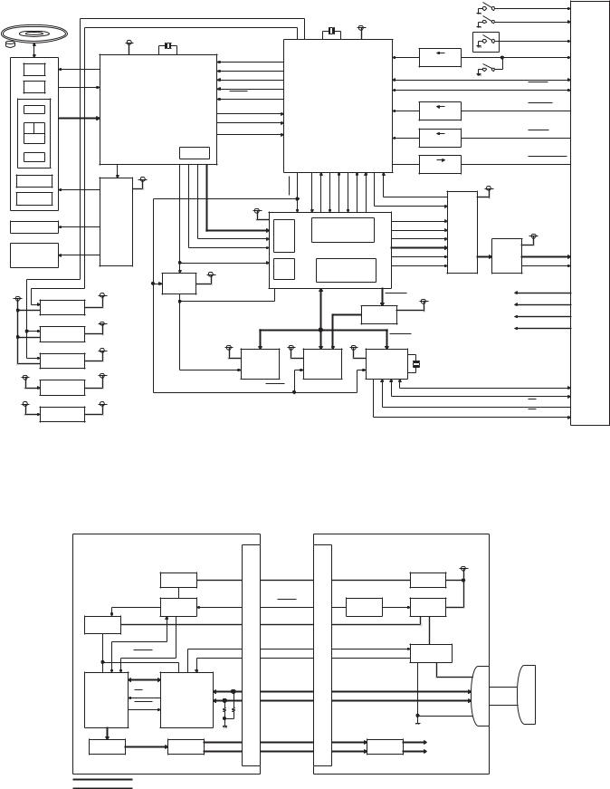
KDC-MP5033U/MP532U KDC-W534UA/UAY/UG/UGY/W5534U/UY
BLOCK DIAGRAM
CD PLAYER UNIT (X32-5830-00)
|
|
SW3.3V |
X1 |
|
|
|
16.893MHz |
||
|
|
|
|
|
|
DPU1 |
IC2 |
|
|
|
|
|
|
|
LD |
|
|
|
|
PD |
|
|
|
|
E |
|
|
SERVO DSP |
|
|
|
|
|
|
A |
B |
|
|
|
C |
|
|
|
|
F |
|
|
|
I2S |
|
|
|
|
|
TR COIL |
IC4 |
S7.5V |
|
|
|
|
|
||
FO COIL |
|
|
|
|
DM1 |
|
MOTOR |
|
|
|
DRIVER |
|
|
|
SP MOTOR |
|
|
||
|
|
|
||
DM2 |
|
|
|
|
LOADING & |
|
|
|
|
SLED |
|
|
|
|
MOTOR |
|
|
IC28 |
|
CS POWER |
|
|
||
|
|
3-STATE |
||
POWER |
|
|
||
SW3.3V |
|
BUFFER |
||
D5V |
|
|
||
IC5 |
|
|
||
|
|
|
||
|
|
|
|
|
|
SW3.3V |
|
|
|
|
IC21 |
CS3.3V |
|
|
|
|
|
|
|
|
3V REG |
|
|
|
|
IC20 |
CS1.8V |
|
|
|
|
|
|
|
|
1.8V REG |
|
|
|
A8V |
IC14 |
SW A5V |
|
|
|
|
|
|
|
|
A5V REG |
|
|
|
BU5V |
IC19 |
BU3.3V |
|
|
|
|
|
|
|
|
BU3.3V REG |
|
|
|
to X34-
|
|
|
|
|
|
|
|
|
S1 |
LOS-SW |
CS POWER |
|
|
X2 |
|
|
|
|
|
S2 |
12EJE-SW |
POWER ON |
|
11.500MHz BU3.3V |
|
|
|
|
|
|
||
|
IC1 |
|
|
|
|
|
|
0-01 |
|
8EJE-SW |
|
|
|
|
|
|
|
Q7 |
ONLY |
S4 |
|
|
|
|
|
|
|
|
|
|
||
|
|
|
|
|
|
|
3.3 |
5V |
LOE/LIM- |
|
A0 |
|
|
|
|
|
|
|
|||
|
|
|
|
|
|
(SW3.3V) |
S3 |
|
||
SI |
|
|
|
|
|
|
|
|||
|
|
|
|
|
|
|
|
|
||
|
|
|
|
|
|
|
|
|
|
|
STB |
|
|
|
|
|
|
|
|
|
I2CDATA |
SCK |
|
|
|
|
|
|
|
|
|
I2CCLK |
RESET |
|
|
|
|
|
|
Q6 |
|
|
|
|
|
|
u-COM |
|
|
|
|
|
|
|
SO |
|
|
|
|
|
3.3 |
5V |
|
MRESET |
|
|
|
|
|
|
|
(BU5V) |
|
|
||
INTQ |
|
|
|
|
|
|
|
|
||
|
|
|
|
|
|
R6,8 |
|
|
|
|
DA EMPH |
|
|
|
|
|
|
|
|
|
|
|
|
|
|
|
|
3.3 |
5V |
|
MSTOP |
|
|
|
|
|
|
|
|
|
|||
|
|
|
|
|
|
|
RESISTOR |
|
|
|
|
|
|
|
|
|
|
Q3 |
|
|
|
|
|
|
|
|
|
|
3.3 |
5V |
|
AUDIO MUTE |
|
|
|
|
|
|
|
(BU5V) |
|
|
|
CS3.3V |
CSRST |
MUTEDATA DATAS |
DATAB CLK SREQ BREQ EMPHCS |
|
EMPH |
|
|
SW A5V |
|
|
|
|
IC18 |
CS3.3V |
|
||||||
|
|
|
|
|
|
|
|
|
||
|
|
|
|
|
INFINITY 0 DET. |
|
|
|||
|
|
|
|
|
|
|
|
|||
& |
IC15 |
|
|
|
|
|
|
|
|
|
|
|
|
|
|
|
|
|
|
|
|
CS1.8V |
|
|
|
|
|
DAC RST |
|
|
|
|
DATA |
|
|
SER2 (3/4WIRE) |
|
|
DAC MUTE |
DAC |
|
SW A8V |
|
LRCK |
CD I/F |
|
|
|
PCM XCK |
IC13 |
||||
|
|
|
|
|
|
|||||
BCLK |
|
|
AUDIO DSP |
|
|
PCM DATA |
|
|
|
|
|
|
|
|
|
PCM LRCK |
|
LPF |
AUDIO Lch |
||
C16 |
|
|
|
|
|
|
||||
|
|
|
|
|
PCM BCLK |
|
AUDIO Rch |
|||
|
PLL |
|
MEMORY |
|
|
|
|
|||
CS3.3V |
|
|
|
|
|
|
|
|
||
|
|
|
CONTROLLER |
|
|
|
|
|
|
|
|
|
|
|
|
|
|
CS3.3V |
|
|
BU5V |
CKO |
|
|
IC26 |
CS, A20 |
|
|
A8V |
|||
|
|
|
|
|
||||||
|
|
|
|
|
|
|
|
|||
|
|
|
|
NAND |
|
|
|
|
D5V (D4V) |
|
|
|
|
|
GATE |
|
|
|
|
S7.5V |
|
|
|
|
|
|
|
|
|
|
|
|
CS3.3V IC16 |
CS3.3V IC17 |
CS3.3V |
IC25 |
|
USB CS |
|
|
|
|
|
|
|
|
|
|
|
|||||
SDRAM |
FLASH |
USB |
|
X3 |
|
|
|
|||
MEMORY |
|
|
|
|
||||||
64Mbit |
DRIVER |
6.00MHz |
|
|
|
|||||
8Mbit |
|
|
|
|
||||||
|
|
|
|
|
|
|
|
|
||
|
CSRST |
|
|
|
|
UHC124 |
|
|
USB D+ |
|
|
|
|
|
|
|
|
|
|
USB D- |
|
|
|
|
|
|
|
|
|
|
|
|
|
|
|
|
|
|
|
|
|
|
OC |
|
|
|
|
|
|
|
|
|
|
PO |
CD PLAYER UNIT (X32-)
|
IC19 |
|
|
BU3.3V |
|
|
IC1 |
|
P-ON |
MECHA- |
|
IC20,21 |
u-COM |
|
CS3.3V |
|
|
(CS1.8V) |
|
|
CSRST |
|
|
IC15 |
IC25 |
|
INT |
USB HOST |
|
DSP |
CONTROLLER |
|
RESET |
||
|
||
IC18 |
IC13 |
|
DAC |
LFP |
|
|
ELECTRIC UNIT (X34-) |
|
|
|
CN1 |
|
CN1 |
|
|
|
|
|
|
BU14V |
|
|
|
|
|
Q1,2 |
|
|
|
BU5V |
|
BU5V |
|
|
|
|
|
|
|
|
|
|
IC101 |
IC2 |
|
|
|
MSTOP |
SESTEM P-ON |
5V |
|
|
|
|
u-COM |
SW-REG. |
|
|
CONNECTOR |
D5V |
CONNECTOR |
|
|
USB CONNECTOR |
POWER ON SW |
IC3 (V-BUS 5V) |
|
|||
|
|
HIGH-SIDE |
|
|
|
|
OVER CURRENT |
|
|
|
|
|
|
SWITCH |
|
|
|
|
|
|
|
|
|
|
|
|
CN2 |
|
|
|
|
|
USB 5V |
|
|
|
USB D+ |
|
USB D+ |
|
|
|
USB D- |
|
USB D- |
CABLE |
|
|
|
|
USB GND |
|
|
|
Lch |
IC10 |
|
|
|
|
|
|
|
|
|
|
Rch |
E-VOL |
|
|
|
USB LINE AUDIO LINE
3
KDC-MP5033U/MP532U
KDC-W534UA/UAY/UG/UGY/W5534U/UY
COMPONENTS DESCRIPTION
● ELECTRIC UNIT (X34-412x-xx)
Ref. No. |
Application / Function |
Operation / Condition / Compatibility |
|
|
|
|
|
IC1 |
Power Supply IC |
DC5V x 1, 7.9V x 1, 8.1V x 2, 10.2V x 1, P-CON, P-ANT output. |
|
|
|
|
|
IC2 |
Power Supply IC |
DC5V for CD mechanism unit and USB. |
|
|
|
|
|
IC3 |
Hi-side SW |
USB5V on when the pin 1 goes “Hi”. |
|
|
|
|
|
IC10 |
E-VOL & Tuner |
E-VOL, Tuner, Stereo decoder. |
|
|
|
|
|
IC101 |
System -COM |
Controls system. |
|
|
|
|
|
IC102 |
Reset IC |
“Lo” when detection voltage is below 3.6V. |
|
|
|
|
|
IC103 |
E2PROM |
Saves and loads for tuner adjustment data. |
|
|
|
|
|
IC201 |
Power IC |
Amplifies signal. |
|
|
|
|
|
IC400 |
RDS Decoder |
Decodes RDS. |
|
|
|
|
|
Q1 |
SERVO+B AVR |
Darlington connection with Q2. (Current buffer) |
|
|
|
|
|
Q2 |
SERVO+B AVR |
Outputs 7.5V. |
|
|
|
|
|
Q3 |
14V SW |
“ON” when the base goes “Hi”. |
|
|
|
|
|
Q4 |
VFD+B & LED AVR |
Darlington connection with Q5. (Current buffer) |
|
|
|
|
|
Q5 |
VFD+B & LED AVR |
Outputs 11V. |
|
|
|
|
|
Q6 |
VFD+B & LED SW |
“ON” when the base goes “Hi”. |
|
|
|
|
|
Q7 |
Non Back Up 5V SW |
“ON” when the base goes “Lo”. |
|
|
|
|
|
Q8 |
Control SW for IC1 |
|
|
|
|
|
|
Q9 |
Serge Protect for IC2 |
Darlington connection with Q5. (Current buffer) |
|
|
|
|
|
Q10 |
Serge Protect for IC2 |
Outputs 15V when back up voltage is over 16V. |
|
|
|
|
|
Q11 |
Control SW for IC2 |
IC2 turns on when the base goes “Lo”. |
|
|
|
|
|
Q12 |
FL FIL Voltage SW |
FL FIL voltage ON/OFF SW. |
|
|
|
|
|
Q13 |
Control SW for Q12 |
Q12 turn on when the base goes “Hi”. |
|
|
|
|
|
Q51 |
Serge DET |
“ON” when the base goes “Hi”. |
|
|
|
|
|
Q52 |
BU DET |
“ON” when the base goes “Hi” during BU is applied. |
|
|
|
|
|
Q53 |
ILLUMI SW |
“ON” when the base goes “Hi”. |
|
|
|
|
|
Q54 |
ACC DET |
“ON” when the base goes “Hi” during ACC is applied. |
|
|
|
|
|
Q101 |
PANEL5V SW |
“ON” when the base goes “Lo”. |
|
|
|
|
|
Q102 |
Control SW for D111 |
D111 is ON when the base goes “Hi”. |
|
|
|
|
|
Q103,104 |
Mute Control |
“ON” when the base goes “Hi”. |
|
|
|
|
|
Q105 |
Mute Driver for Preout |
“ON” when the base goes “Lo”. |
|
|
|
|
|
Q201,202 |
DC Offset DET SW |
“ON” when the base goes “Lo”. (At that time, IC201’s SP-OUT DC is |
|
separated) |
|||
|
|
||
|
|
|
|
Q203 |
DC Offset DET |
“ON” when the base goes “Hi”. (At that time, Q201 and Q202’s outputs |
|
are separated) |
|||
|
|
||
|
|
|
|
Q204 |
SVR Discharge |
IC201’s pin 10 discharges when the base goes “Hi”. |
|
|
|
|
|
Q251 |
Mute SW for Lch Preout |
Pre-output is muted when the base goes “Hi”. |
|
|
|
|
|
Q252 |
Mute SW for Rch Preout |
Pre-output is muted when the base goes “Hi”. |
|
|
|
|
|
Q400 |
Buffer |
IC10 QUAL output buffer. |
|
|
|
|
|
Q501 |
AM RF Amplifier |
Adjusts for gain. |
|
|
|
|
|
Q502 |
FM RF Amplifier |
Amplifies RF. |
|
|
|
|
|
Q503,504 |
AFS Control |
Controls AFS time. |
|
|
|
|
4
KDC-MP5033U/MP532U
KDC-W534UA/UAY/UG/UGY/W5534U/UY
COMPONENTS DESCRIPTION
● SWITCH UNIT (X16-373x-xx)
Ref. No. |
Application / Function |
Operation / Condition / Compatibility |
|
|
|
IC2 |
Remote Control IC |
|
|
|
|
Q4,5 |
SW5V |
The power supply of IC2 is turned on when Q5’s base level goes “Hi”. |
|
|
|
Q10 |
GREEN SW |
When the base goes “Hi”, LED lights. |
|
|
|
Q12~14 |
Grid Driver |
Each grid is ON when each transistor’s base is “Lo”. |
|
|
|
Q15 |
RED SW |
When the base goes “Hi”, LED lights. |
|
|
|
Q20 |
Key Scan Start SW |
Key scan starts when the base goes “Hi”. |
|
|
|
● DAUGHTER UNIT (X89-2902-70): KDC-MP5033U/MP532U/W5534U/W5534UY only
Ref. No. |
Application / Function |
Operation / Condition / Compatibility |
|
|
|
Q221,222 |
2-PREOUT MUTE |
“ON” when the base goes “H”. |
|
|
|
Q225 |
2-PREOUT MUTE |
“ON” when the base goes “H”. |
|
|
|
● CD PLAYER UNIT (X32-5830-00)
Ref. No. |
Application / Function |
Operation / Condition / Compatibility |
|
|
|
|
|
IC1 |
Mechanism µ-COM |
|
|
|
|
|
|
IC2 |
Signal Processor |
|
|
|
|
|
|
IC4 |
BTL Driver |
|
Spindel motor, sled (including loading & eject) motor and pick-up actuator |
|
|
|
|
IC5 |
SW3.3V Regulator |
3.3V power supply for IC2, pick-up, IC18 digital part |
|
|
|
|
|
IC13 |
Audio Active Filter |
2nd LPF |
|
|
|
|
|
IC14 |
A5V Regulator |
|
3.3V power supply for DAC |
|
|
|
|
IC15 |
DSP for Compression Audio Decoder |
ACDrive decoder, MP3/WMA/AAC decoder |
|
|
|
|
|
IC16 |
Compression Audio Codec SDRAM |
|
|
|
|
|
|
IC17 |
Decoder Software & Unique ID Strage Flash ROM |
|
|
|
|
|
|
IC18 |
Audio D-A Converter (24-bit external) |
External 24-bit for audio |
|
|
|
|
|
IC19 |
BU3.3V Regulator |
3.3V power supply for µ-com |
|
|
|
|
|
IC20 |
1.8V Regulator |
|
1.8V power supply for IC15 core part |
|
|
|
|
IC21 |
Decoder/SDRAM/Flash ROM/USB Driver 3.3V |
Power supply for decoder, SDRAM, flash ROM and USB driver. |
|
Regulator |
|
3.3V power supply for IC15 port parts, IC16, IC17, IC25, IC26 and IC28. |
|
|
|
||
|
|
|
|
IC25 |
USB Host Controller |
|
|
|
|
|
|
IC26 |
Switching among IC15 & Flash ROM & SDRAM & USB |
For DSP for Compression Audio Decoder, Flash ROM, SDRAM and USB |
|
|
|
|
|
IC28 |
Clock SW |
|
To SDRAM |
|
|
|
|
Q3 |
Level Shift 3.3V→ |
5V |
|
|
|
|
|
Q6,7 |
Level Shift 3.3V← |
5V |
|
|
|
|
|
Q8 |
APC (Auto Power Control) |
|
|
|
|
|
|
Q9,10 |
Anticipation Sub-beam Delay |
During non-searching |
|
|
|
|
|
Q16 |
Logic Inverter |
|
µ-com “ZERO” terminal |
|
|
|
|
Q17 |
USB Hi-side SW |
|
|
|
|
|
|
D2 |
Static Electricity Countermeasure |
For IC2 built-in reset terminal |
|
|
|
|
|
D3 |
Laser Diode Protection |
|
|
|
|
|
|
D9 |
Static Electricity Countermeasure |
|
|
|
|
|
|
5
KDC-MP5033U/MP532U KDC-W534UA/UAY/UG/UGY/W5534U/UY
MICROCOMPUTER’S TERMINAL DESCRIPTION
● SYSTEM -COM: IC101 on X34- (ELECTRIC UNIT)
Pin No. |
|
Pin Name |
I/O |
Application |
Truth |
Processing / Operation / Description |
||||
|
Value Table |
|||||||||
|
|
|
|
|
|
|
|
|
|
|
|
|
|
|
|
|
|
|
|
|
|
1 |
|
|
|
|
|
I |
ACC power supply detection |
|
L: ACC found, H: No ACC |
|
|
ACC DET |
|
|
|
||||||
|
|
|
|
|
|
|
|
|
|
|
2 |
|
|
|
|
I |
Momentary power down detection |
|
L: BU found, H: No BU or momentary power down |
||
|
BU DET |
|
|
|
|
|||||
|
|
|
|
|
|
|
|
|
|
|
3 |
|
|
|
I |
Dimmer illumination detection |
|
L: ON, H: OFF |
|||
|
ILLUMI DET |
|
|
|||||||
|
|
|
|
|
|
|
|
|
|
|
4 |
|
REMO |
I |
Remote control signal input |
|
Detects pulse width |
||||
|
|
|
|
|
|
|
|
|
|
|
5 |
|
NC |
- |
Not used |
|
Output L fixed |
||||
|
|
|
|
|
|
|
|
|
|
|
6 |
|
BYTE |
- |
|
|
|
||||
|
|
|
|
|
|
|
|
|
|
|
7 |
|
CNVSS |
- |
|
|
|
||||
|
|
|
|
|
|
|
|
|
|
|
8 |
|
XCIN |
I |
32.768kHz |
|
|
||||
|
|
|
|
|
|
|
|
|
|
|
9 |
|
XCOUT |
I |
32.768kHz |
|
|
||||
|
|
|
|
|
|
|
|
|
|
|
10 |
|
RESET |
- |
|
|
|
||||
|
|
|
|
|
|
|
|
|
|
|
11 |
|
XOUT |
- |
12.0MHz |
|
|
||||
|
|
|
|
|
|
|
|
|
|
|
12 |
|
VSS |
- |
|
|
|
||||
|
|
|
|
|
|
|
|
|
|
|
13 |
|
XIN |
- |
12.0MHz |
|
|
||||
|
|
|
|
|
|
|
|
|
|
|
14 |
|
VCC1 |
- |
|
|
|
||||
|
|
|
|
|
|
|
|
|
|
|
15 |
|
NMI |
- |
Not used |
|
|
||||
|
|
|
|
|
|
|
|
|
|
|
16 |
|
|
I |
Panel communication detection |
|
H: Panel opened, L: Panel closed |
||||
|
CN DET |
|
|
|||||||
|
|
|
|
|
|
|
|
|
|
|
17 |
|
RDS CLK |
I |
RDS decoder clock input |
|
|
||||
|
|
|
|
|
|
|
|
|
|
|
18 |
|
LX REQ S |
I |
Communication request from slave unit |
|
|
||||
|
|
|
|
|
|
|
|
|
|
|
19 |
|
AUD MUTE |
O |
Mute control for IC10 and preout |
|
|
||||
|
|
|
|
|
|
|
|
|
|
|
20 |
|
PWIC STBY |
O |
Power IC standby control |
|
H: POWER ON, L: POWER OFF |
||||
|
|
|
|
|
|
|
|
|
|
|
21 |
|
PWIC SVR |
O |
SVR discharge circuit |
|
SVR discharge circuit |
||||
|
|
|
|
|
|
|
|
|
|
|
22 |
|
PWIC MUTE |
O |
Power IC mute |
|
STANDBY source or momentary power down: L |
||||
|
|
TEL mute: L |
||||||||
|
|
|
|
|
|
|
|
|
|
|
|
|
|
|
|
|
|
|
|
|
|
23 |
|
LX REQ M |
O |
Communication request to slave unit |
|
|
||||
|
|
|
|
|
|
|
|
|
|
|
24 |
|
LX CON |
O |
Start-up request to slave unit |
|
H: Slave unit starts up, L: Slave unit stops |
||||
|
|
|
|
|
|
|
|
|
|
|
25 |
|
LX RST |
O |
Fouced reset to slave unit |
|
H: Reset, L: Normal |
||||
|
|
|
|
|
|
|
|
|
|
|
26 |
|
PWIC BEEP |
O |
Beep output |
|
|
||||
|
|
|
|
|
|
|
|
|
|
|
27 |
|
TUN SCL |
I/O |
Front-end I2C clock input and output |
|
MAX400kHz |
||||
|
|
|
|
|
|
|
|
|
|
|
28 |
|
TUN SDA |
I/O |
Front-end I2C data input and output |
|
|
||||
|
|
|
|
|
|
|
|
|
|
|
29 |
|
VFD DATA |
I/O |
VFD data input and output |
|
Data input and output |
||||
|
|
|
|
|
|
|
|
|
|
|
30 |
|
VFD INT |
I |
VFD INT input |
|
INT input |
||||
|
|
|
|
|
|
|
|
|
|
|
31 |
|
VFD CLK |
O |
VFD clock output |
|
125kHz |
||||
|
|
|
|
|
|
|
|
|
|
|
|
|
|
|
|
|
|
|
|
|
H: Reset cancelled, L: Reset |
32 |
|
VFD RST |
O |
VFD driver reset |
|
L: Momentary power down, panel detached or 11 |
||||
|
|
|
|
|
|
|
|
|
|
minutes after ACC OFF |
|
|
|
|
|
|
|
|
|
|
|
33 |
|
LX DATA M |
I/O |
Data to slave unit |
|
|
||||
|
|
|
|
|
|
|
|
|
|
|
34 |
|
LX DATA S |
I |
Data from slave unit |
|
|
||||
|
|
|
|
|
|
|
|
|
|
|
35 |
|
LX CLK |
I/O |
LX-BUS clock |
|
|
||||
|
|
|
|
|
|
|
|
|
|
|
36 |
|
VFD KEY REQ |
I |
Communication request from VFD driver |
|
Connects to INT |
||||
|
|
|
|
|
|
|
|
|
|
|
|
|
|
|
|
|
|
|
|
|
H: Normal, L: FM/AM seek or AF search |
37 |
|
RDS AFS L 2 |
O |
RDS mute output |
q |
(L: Tuner SRC or Auto Zero) |
||||
|
|
|
|
|
|
|
|
|
|
*Same process as RDS AFS L (Pin 38) |
|
|
|
|
|
|
|
|
|
|
|
38 |
|
RDS AFS L |
O |
RDS mute output |
q |
H: Normal, L: FM/AM seek or AF search |
||||
|
(L: Tuner SRC or Auto Zero) |
|||||||||
|
|
|
|
|
|
|
|
|
|
|
|
|
|
|
|
|
|
|
|
|
|
6
KDC-MP5033U/MP532U KDC-W534UA/UAY/UG/UGY/W5534U/UY
MICROCOMPUTER’S TERMINAL DESCRIPTION
Pin No. |
|
Pin Name |
I/O |
Application |
Truth |
Processing / Operation / Description |
|||||
|
Value Table |
||||||||||
|
|
|
|
|
|
|
|
|
|
|
|
|
|
|
|
|
|
|
|
|
|
|
|
39 |
|
EPM |
I |
Flash EPM input |
|
|
|||||
|
|
|
|
|
|
|
|
|
|
|
|
40 |
TUN SD |
I |
Search stop input |
|
H: Station found, L: No station |
||||||
|
|
|
|
|
|
|
|
|
|
|
|
41 |
|
TUN FANC OUT |
O |
Tuner block (in -com) check |
|
H: E2P OK in test mode, L: E2P NG in test mode |
|||||
|
|
L: Normal |
|||||||||
|
|
|
|
|
|
|
|
|
|
|
|
|
|
|
|
|
|
|
|
|
|
|
|
42 |
TUN ADJ |
I |
E2PROM writing request and IC10 adjustment |
|
E2PROM writing at ADJ=H |
||||||
|
|
|
|
|
|
|
|
|
|
|
|
43 |
NC |
- |
Not used |
|
Output L fixed |
||||||
|
|
|
|
|
|
|
|
|
|
|
|
44 |
|
VFD CE |
O |
VFD chip select control |
|
|
|||||
|
|
|
|
|
|
|
|
|
|
|
|
45 |
|
RDS QUAL |
I |
RDS decoder QUAL input |
|
|
|||||
|
|
|
|
|
|
|
|
|
|
|
|
46 |
RDS DATA |
I |
RDS decoder data input |
|
|
||||||
|
|
|
|
|
|
|
|
|
|
|
|
47,48 |
|
NC |
- |
Not used |
|
Output L fixed |
|||||
|
|
|
|
|
|
|
|
|
|
|
|
49 |
DSI |
I/O |
DSI/EJECT LED control |
|
OFF: Hi-z, Pulse drive: Panel detached |
||||||
|
H: Illumination ON or panel opened (POWER ON) |
||||||||||
|
|
|
|
|
|
|
|
|
|
|
|
|
|
|
|
|
|
|
|
|
|
|
|
50 |
|
|
|
|
|
I |
Eject key input |
|
L: Eject |
||
|
EJECT |
|
|
|
|
|
|
||||
|
|
|
|
|
|
|
|
|
|
|
|
51 |
ENC CCW |
I |
Encoder input (Counterclockwise) |
|
Detects pulse width |
||||||
|
|
|
|
|
|
|
|
|
|
|
|
52 |
|
ENC CW |
I |
Encoder input (Clockwise) |
|
Detects pulse width |
|||||
|
|
|
|
|
|
|
|
|
|
|
|
|
|
|
|
|
|
|
|
|
|
|
L: ON, Hi-Z: Momentary power down, panel detached |
53 |
PON PANEL |
I/O |
Panel 5V control |
|
|||||||
|
or 11 minutes after ACC OFF |
||||||||||
|
|
|
|
|
|
|
|
|
|
|
|
|
|
|
|
|
|
|
|
|
|
|
|
54~59 |
|
NC |
- |
Not used |
|
Output L fixed |
|||||
|
|
|
|
|
|
|
|
|
|
|
|
60 |
|
VCC2 |
- |
|
|
|
|||||
|
|
|
|
|
|
|
|
|
|
|
|
|
|
|
|
|
|
|
|
|
|
||
61 |
PON 5V |
O |
SW5V control |
|
L: POWER ON, H: POWER OFF |
||||||
|
|
|
|
|
|
|
|
|
|
|
|
62 |
VSS |
- |
|
|
|
||||||
|
|
|
|
|
|
|
|
|
|
|
|
63 |
CD DISC12 SW |
I |
12cm CD detection |
|
|
||||||
|
|
|
|
|
|
|
|
|
|
|
|
64 |
|
CD LOS SW |
I |
CD loading detection |
|
|
|||||
|
|
|
|
|
|
|
|
|
|
|
|
65 |
CD SCL |
I/O |
CD mechanism I2C clock output |
|
|
||||||
|
|
|
|
|
|
|
|
|
|
|
|
66 |
CD SDA |
I/O |
CD mechanism I2C data input and output |
|
|
||||||
|
|
|
|
|
|
|
|
|
|
|
|
67 |
|
CD MUTE |
I |
CD mute request |
|
H: Normal, L: Mute request |
|||||
|
|
(CD playing time only) |
|||||||||
|
|
|
|
|
|
|
|
|
|
|
|
|
|
|
|
|
|
|
|
|
|
|
|
68 |
|
|
|
O |
CD mechanism -com reset |
|
H: Normal, L: Reset |
||||
|
CD MRST |
|
|
|
|||||||
|
|
|
|
|
|
|
|
|
|
|
|
|
|
|
|
|
|
|
|
|
CD mechanism -com stop |
|
H: Mechanism -com operates |
69 |
|
CD MSTOP |
O |
|
|||||||
|
|
L: Mechanism -com stops |
|||||||||
|
|
|
|
|
|
|
|
|
|
|
|
|
|
|
|
|
|
|
|
|
|
|
|
70 |
CD DISC8 SW |
I |
8cm CD detection (Not used) |
|
|
||||||
|
|
|
|
|
|
|
|
|
|
|
|
71 |
CD LOE LIM SW |
I |
CD detection (Chucking SW) |
|
H: Loading completes, L: No disc |
||||||
|
|
|
|
|
|
|
|
|
|
|
|
72 |
|
CD LOEJ |
I/O |
CD motor control |
w |
Refer to the truth value table |
|||||
|
|
|
|
|
|
|
|
|
|
|
|
73 |
|
CD MOTOR |
O |
CD motor control |
w |
Refer to the truth value table |
|||||
|
|
|
|
|
|
|
|
|
|
|
|
74 |
PANEL DET |
I |
Panel detection |
|
L: No panel, H: Panel attached |
||||||
|
|
|
|
|
|
|
|
|
|
|
|
75~77 |
|
NC |
- |
Not used |
|
Output L fixed |
|||||
|
|
|
|
|
|
|
|
|
|
|
|
78 |
TUN TYPE2 |
I |
Destination setting |
e |
Refer to the truth value table |
||||||
|
|
|
|
|
|
|
|
|
|
|
|
79 |
TUN TYPE1 |
I |
Destination setting |
e |
Refer to the truth value table |
||||||
|
|
|
|
|
|
|
|
|
|
|
|
80 |
RDS NOISE |
I |
FM noise detection |
|
|
||||||
|
|
|
|
|
|
|
|
|
|
|
|
81 |
|
TUN SMETER |
I |
S-meter input |
|
|
|||||
|
|
|
|
|
|
|
|
|
|
|
|
82 |
TYPE 3 |
I |
Destination SW |
r |
Refer to the truth value table |
||||||
|
|
|
|
|
|
|
|
|
|
|
|
83 |
TYPE 2 |
I |
Destination SW |
r |
Refer to the truth value table |
||||||
|
|
|
|
|
|
|
|
|
|
|
|
84 |
TYPE 1 |
I |
Destination SW |
r |
Refer to the truth value table |
||||||
|
|
|
|
|
|
|
|
|
|
|
|
85 |
LINE MUTE |
I |
Line mute detection |
|
TEL mute: Below 1V , NAVI mute: Over 2.5V |
||||||
|
|
|
|
|
|
|
|
|
|
|
|
7
KDC-MP5033U/MP532U KDC-W534UA/UAY/UG/UGY/W5534U/UY
MICROCOMPUTER’S TERMINAL DESCRIPTION
Pin No. |
|
Pin Name |
I/O |
Application |
Truth |
Processing / Operation / Description |
|
|
Value Table |
||||||
|
|
|
|
|
|
|
|
|
|
|
|
|
|
|
|
|
|
|
|
|
|
|
If DC offset is found 10 times in 100m seconds with |
86 |
PWIC DC DET |
I |
DC offset detection |
|
condition of over 1.0V, it will be judged as DC offset |
||
|
|
|
|
|
|
|
detected. |
|
|
|
|
|
|
|
|
87 |
|
O |
Power supply for CD mechanism and USB |
|
L: POWER ON, H: POWER OFF |
||
|
PON CD |
|
|
||||
|
|
|
|
|
|
|
|
88 |
NC |
- |
Not used |
|
Output L fixed |
||
|
|
|
|
|
|
|
|
89 |
PON FL |
O |
FL+B control |
|
H: FL+B ON, L: FL+B OFF |
||
|
|
|
|
|
|
|
|
90 |
PS1 3 |
O |
Power supply IC (IC1) control 1-3 |
t |
Refer to the truth value table |
||
|
|
|
|
|
|
|
|
91 |
PS1 2 |
O |
Power supply IC (IC1) control 1-2 |
t |
Refer to the truth value table |
||
|
|
|
|
|
|
|
|
92 |
PS1 1 |
O |
Power supply IC (IC1) control 1-1 |
t |
Refer to the truth value table |
||
|
|
|
|
|
|
|
|
93 |
PS2 2 |
O |
Power supply IC (IC1) control 2-2 |
t |
Refer to the truth value table |
||
|
|
|
|
|
|
|
|
94 |
AVSS |
- |
|
|
|
||
|
|
|
|
|
|
|
|
95 |
REF CON |
O |
VREF control |
|
Connects to VREF |
||
|
|
|
|
|
|
|
|
96 |
VREF |
- |
|
|
|
||
|
|
|
|
|
|
|
|
97 |
AVCC |
- |
|
|
Connects to VCC |
||
|
|
|
|
|
|
|
|
98 |
PS2 1 |
O |
Power supply IC (IC1) control 2-1 |
t |
Refer to the truth value table |
||
|
|
|
|
|
|
|
|
99,100 |
NC |
- |
Not used |
|
Output L fixed |
||
|
|
|
|
|
|
|
|
Truth value table q AFS CONTROL
|
RDS AFS L |
Condition |
|
|
|
AFS LOW |
L |
No sound output with AF search |
|
|
|
AFS MID |
Hi-Z |
Sound output with AF search |
|
|
|
AFS HIGH |
Hi-Z |
Normal reception |
|
|
|
w CD MOTOR CONTROL |
|
|
|
|
|
|
CD MOTOR |
CD LOADING/EJECT |
|
|
|
Stop |
L |
L |
|
|
|
Load |
H |
L |
|
|
|
Eject |
H |
H |
|
|
|
Brake |
H |
Hi-z |
|
|
|
e TUNER TYPE
|
TUN TYPE1 |
TUN TYPE2 |
|
(Pin 79) |
(Pin 78) |
|
|
|
Kenwood brand model |
L |
L |
|
|
|
OEM model 1 |
L |
H |
|
|
|
OEM model 2 |
H |
L |
|
|
|
OEM model 3 |
H |
H |
r DESTINATION SW
TYPE 1 |
TYPE 2 |
|
TYPE 3 |
DESTI- |
|
MODEL |
|
||||||
(Pin 84) |
(Pin 83) |
|
(Pin 82) |
NATION |
|
|
|||||||
|
|
|
|
|
|||||||||
|
|
|
|
|
|
|
|
|
|
|
|
|
|
L |
|
H |
|
|
L |
|
E |
|
KDC-W5534U/UY |
|
|||
|
|
|
|
|
|
|
|
|
|
|
|
|
|
H |
|
H |
|
|
L |
|
E |
|
KDC-W534UA/UAY/UG/UGY |
||||
|
|
|
|
|
|
|
|
|
|
|
|
|
|
L |
|
L |
|
|
L |
|
K |
|
KDC-MP532U |
|
|||
|
|
|
|
|
|
|
|
|
|
|
|
|
|
H |
|
L |
|
|
H |
|
M |
|
KDC-MP5033U |
|
|||
|
|
|
|
|
|
|
|
|
|
|
|
|
|
H |
|
H |
|
|
H |
|
J |
|
U515 |
|
|
|
|
|
|
|
|
|
|
|
|
|
|
|
|||
t POWER SUPPLY IC (IC1) CONTROL |
|
|
|
||||||||||
SW1 (Pin 10) |
|
|
|
|
|
|
|
|
|
|
|||
|
|
|
|
|
|
|
|
|
|
||||
PS1-1 |
|
PS1-2 |
|
PS1-3 |
|
|
AUDIO |
P-CON |
P-ANT |
||||
|
|
|
|
|
|
|
|
|
|
|
|
|
|
L |
|
L |
|
L |
|
|
|
OFF |
OFF |
|
OFF |
||
H |
|
L |
|
L |
|
|
|
ON |
OFF |
|
OFF |
||
L |
|
H |
|
L |
|
|
|
ON |
OFF |
|
OFF |
||
H |
|
H |
|
H |
|
|
|
ON |
ON |
|
ON |
||
SW2 (Pin 11) |
|
|
|
|
|
|
|
|
|
|
|||
|
|
|
|
|
|
|
|
|
|
|
|||
PS2-1 |
|
PS2-2 |
|
ILLUMI |
|
|
FM |
AM |
|
|
|||
|
|
|
|
|
|
|
|
|
|
|
|||
L |
|
L |
|
OFF |
|
|
OFF |
OFF |
|
|
|||
H |
|
L |
|
ON |
|
|
ON |
OFF |
|
|
|||
H |
|
H |
|
ON |
|
|
ON |
ON |
|
|
|||
|
|
|
|
|
|
|
|
|
|
|
|
|
|
8
KDC-MP5033U/MP532U KDC-W534UA/UAY/UG/UGY/W5534U/UY
MICROCOMPUTER’S TERMINAL DESCRIPTION
● MECHANISM -COM: IC1 (X32-: CD PLAYER UNIT)
Pin No. |
|
Pin Name |
I/O |
Application |
Processing / Operation / Description |
||||||||
|
|
|
|
|
|
|
|
|
|
|
|
|
|
1~5 |
|
NC |
- |
Not used |
Opened output L fixed |
||||||||
|
|
|
|
|
|
|
|
|
|
|
|
|
|
6 |
|
BYTE |
I |
External data bus SW input |
Connects to GND |
||||||||
|
|
|
|
|
|
|
|
|
|
|
|
|
|
7 |
|
CNVSS |
I |
Processor mode SW |
L: Single chip mode |
||||||||
|
H: Microprocessor mode or flash ROM writing |
||||||||||||
|
|
|
|
|
|
|
|
|
|
|
|
||
|
|
|
|
|
|
|
|
|
|
|
|
|
|
8 |
|
|
|
|
|
|
|
|
O |
Audio mute control |
L: Mute ON, H: Mute OFF |
||
|
MUTE |
|
|
|
|
||||||||
|
|
|
|
|
|
|
|
|
|
|
|
|
|
9 |
|
NC |
- |
Not used |
Opened output L fixed |
||||||||
|
|
|
|
|
|
|
|
|
|
|
|
|
|
10 |
|
|
|
|
|
|
I |
Reset detection |
L: Reset (Flash ROM writing), H: Normal |
||||
|
RESET |
|
|
|
|||||||||
|
|
|
|
|
|
|
|
|
|
|
|
|
|
11 |
XOUT |
O |
Main clock output |
Connects to resonator |
|||||||||
|
|
|
|
|
|
|
|
|
|
|
|
|
|
12 |
VSS |
- |
Power supply input |
Connects to GND |
|||||||||
|
|
|
|
|
|
|
|
|
|
|
|
|
|
13 |
|
XIN |
I |
Main clock input |
Connects to resonator |
||||||||
|
|
|
|
|
|
|
|
|
|
|
|
|
|
14 |
|
VCC1 |
- |
Power supply input |
Connects to BU3.3V |
||||||||
|
|
|
|
|
|
|
|
|
|
|
|
|
|
|
|
|
|
|
|
|
|
|
|
|
|||
15 |
NMI |
I |
NMI interruption input |
Input Hi (Pull-up) fixed |
|||||||||
|
|
|
|
|
|
|
|
|
|
|
|
|
|
16 |
|
|
|
|
|
I |
STANDBY comeback interrupption |
L: Stop, H: Stop cancelled (Hi edge) |
|||||
|
MSTOP |
|
|
||||||||||
|
|
|
|
|
|
|
|
|
|
|
|
|
|
17 |
NC |
- |
Not used |
Opened output L fixed |
|||||||||
|
|
|
|
|
|
|
|
|
|
|
|
|
|
18 |
DSP INT |
I |
DSP interruption signal input |
H: Interruption (Hi edge) |
|||||||||
|
|
|
|
|
|
|
|
|
|
|
|
|
|
19~22 |
|
NC |
- |
Not used |
Opened output L fixed |
||||||||
|
|
|
|
|
|
|
|
|
|
|
|
|
|
23 |
E2P SCL |
I/O |
E2P I2C clock output |
Series resistors and E2PROM are not built when |
|||||||||
ROM collection is not used. |
|||||||||||||
|
|
|
|
|
|
|
|
|
|
|
|
||
|
|
|
|
|
|
|
|
|
|
|
|
|
|
24 |
E2P SDA |
I/O |
E2P I2C data input and output |
Series resistors and E2PROM are not built when |
|||||||||
ROM collection is not used. |
|||||||||||||
|
|
|
|
|
|
|
|
|
|
|
|
||
|
|
|
|
|
|
|
|
|
|
|
|
|
|
25,26 |
|
NC |
- |
Not used |
Opened output L fixed |
||||||||
|
|
|
|
|
|
|
|
|
|
|
|
|
|
27 |
SCL |
I |
System -com I2C clock input |
|
|||||||||
|
|
|
|
|
|
|
|
|
|
|
|
|
|
28 |
|
SDA |
I/O |
System -com I2C data input and output |
|
||||||||
|
|
|
|
|
|
|
|
|
|
|
|
|
|
29 |
DSP TXD |
O |
Data output for DSP serial data |
Flash ROM writing: TXD (Pull-up) |
|||||||||
|
|
|
|
|
|
|
|
|
|
|
|
|
|
30 |
DSP RXD |
I |
Data input for DSP serial data |
Flash ROM writing: RXD |
|||||||||
|
|
|
|
|
|
|
|
|
|
|
|
|
|
31 |
DSP CLK |
O |
Clock output for DSP serial data |
Flash ROM writing: SCLK (Pull-up) |
|||||||||
|
|
|
|
|
|
|
|
|
|
|
|
|
|
32 |
|
DSP STB (BUSY) |
O |
DSP data strove signal output |
Flash ROM writing: BUSY |
||||||||
|
|
|
|
|
|
|
|
|
|
|
|
|
|
33 |
CS SDATA |
O |
Data output for decoder serial data |
|
|||||||||
|
|
|
|
|
|
|
|
|
|
|
|
|
|
34 |
|
CS BDATA |
I |
Data input for decoder serial data |
|
||||||||
|
|
|
|
|
|
|
|
|
|
|
|
|
|
35 |
CS CLK |
O |
Clock output for decoder serial data |
|
|||||||||
|
|
|
|
|
|
|
|
|
|
|
|
|
|
36~38 |
|
NC |
- |
Not used |
Opened output L fixed |
||||||||
|
|
|
|
|
|
|
|
|
|
|
|
|
|
39 |
|
|
|
- |
Not used (Flash ROM: EPM) |
Opened output L fixed |
|||||||
|
EPM |
|
|
||||||||||
|
|
|
|
|
|
|
|
|
|
|
|
|
|
40 |
PON D3.3 |
O |
D3.3V POWER ON control |
H: POWER ON, L: POWER OFF |
|||||||||
|
|
|
|
|
|
|
|
|
|
|
|
|
|
41 |
PON A5 |
O |
A5.0V POWER ON control |
H: POWER ON, L: POWER OFF |
|||||||||
|
|
|
|
|
|
|
|
|
|
|
|
|
|
42 |
PON CS1 |
O |
IC15 series 3.3V POWER ON control |
H: POWER ON, L: POWER OFF |
|||||||||
|
|
|
|
|
|
|
|
|
|
|
|
|
|
43 |
PON CS2 |
O |
IC15 series 1.8V POWER ON control |
H: POWER ON, L: POWER OFF |
|||||||||
|
|
|
|
|
|
|
|
|
|
|
|
|
|
44 |
|
|
- |
Not used (Flash ROM: CE) |
Opened output L fixed |
||||||||
|
CE |
|
|
||||||||||
|
|
|
|
|
|
|
|
|
|
|
|
|
|
|
|
|
|
|
|
|
|||||||
45 |
DRV MUTE |
O |
Driver mute |
L: Stop, H: Mute OFF |
|||||||||
|
|
|
|
|
|
|
|
|
|
|
|
|
|
46,47 |
|
NC |
- |
Not used |
Opened output L fixed |
||||||||
|
|
|
|
|
|
|
|
|
|
|
|
|
|
48 |
|
ZERO M |
I |
0-bit mute detection |
H: Mute ON, L: Mute OFF |
||||||||
|
(No distinction of Lch/Rch) |
||||||||||||
|
|
|
|
|
|
|
|
|
|
|
|
||
|
|
|
|
|
|
|
|
|
|
|
|
|
|
49 |
DE-EMPHASIS |
O |
DAC de-emphasis control |
H: De-emphasis ON, L: De-emphasis OFF |
|||||||||
|
|
|
|
|
|
|
|
|
|
|
|
|
|
50,51 |
|
NC |
- |
Not used |
Opened output L fixed |
||||||||
|
|
|
|
|
|
|
|
|
|
|
|
|
|
52 |
|
LIM SW |
I |
Laser pick-up inner circumference detection |
H: Inner circumference |
||||||||
|
SW signal input |
||||||||||||
|
|
|
|
|
|
|
|
|
|
|
|
||
|
|
|
|
|
|
|
|
|
|
|
|
|
|
9
KDC-MP5033U/MP532U KDC-W534UA/UAY/UG/UGY/W5534U/UY
MICROCOMPUTER’S TERMINAL DESCRIPTION
Pin No. |
|
Pin Name |
I/O |
Application |
Processing / Operation / Description |
|||
|
|
|
|
|
|
|
|
|
53 |
DISC NORMAL |
O |
Media discrimination result output (Not used) |
H: Normal disc, L: Other disc |
||||
|
|
|
|
|
|
|
|
|
54 |
DISC H RW |
O |
Media discrimination result output (Not used) |
H: High reflecting RW disc, L: Other disc |
||||
|
|
|
|
|
|
|
|
|
55 |
DISC RW |
O |
Media discrimination result output (Not used) |
H: Normal RW disc, L: Other disc |
||||
|
|
|
|
|
|
|
|
|
56 |
TEST OUT4 |
O |
Output for test |
Opened output L fixed |
||||
|
|
|
|
|
|
|
|
|
57 |
TEST OUT3 |
O |
Output for test |
Opened output L fixed |
||||
|
|
|
|
|
|
|
|
|
58 |
TEST OUT2 |
O |
Output for test |
Opened output L fixed |
||||
|
|
|
|
|
|
|
|
|
59 |
TEST OUT1 |
O |
Output for test |
Opened output L fixed |
||||
|
|
|
|
|
|
|
|
|
60 |
|
VCC2 |
- |
Power supply input |
Connects to BU3.3V |
|||
|
|
|
|
|
|
|
|
|
61 |
TEST OUT0 |
O |
Output for test |
Opened output L fixed |
||||
|
|
|
|
|
|
|
|
|
62 |
VSS |
- |
Power supply input |
Connects to GND |
||||
|
|
|
|
|
|
|
|
|
63~66 |
|
NC |
- |
Not used |
Opened output L fixed |
|||
|
|
|
|
|
|
|
|
|
67 |
TEST IN3 |
I |
TEST IN3 |
Pull-down connection (L: Normal/H: During test) |
||||
|
|
|
|
|
|
|
|
|
68 |
MODEL SEL |
I |
Model determination |
L: DXM-6810W (X32-583), H: DXM-6820W (X32-587) |
||||
|
|
|
|
|
|
|
|
|
69 |
E2P WRITE |
I |
TEST IN1: E2P writing permission |
Pull-down connection (L: Normal/H: During writing) |
||||
|
|
|
|
|
|
|
|
|
70 |
UNIQ ID |
I |
TEST IN0: Uniqe ID writing permission |
Pull-down connection (L: Normal/H: During writing) |
||||
|
|
|
|
|
|
|
|
|
71~73 |
|
NC |
- |
Not used |
Opened output L fixed |
|||
|
|
|
|
|
|
|
|
|
74 |
SEARCH |
O |
Searching situation output |
H: During seaching, L: Normal |
||||
|
|
|
|
|
|
|
|
|
75,76 |
|
NC |
- |
Not used |
Opened output L fixed |
|||
|
|
|
|
|
|
|
|
|
77 |
|
|
|
O |
DSP reset control |
L: Reset, H: Normal |
||
|
DSP RST |
|
|
|||||
|
|
|
|
|
|
|
|
|
78 |
|
DSP A0 |
O |
DSP command/parameter discrimination signal |
H: During parameter transmitting |
|||
|
output |
L: During command transmitting |
||||||
|
|
|
|
|
|
|
||
|
|
|
|
|
|
|
|
|
79 |
DA EMPHASIS |
I |
DSP DA emphasis input |
H: emphasis ON, L: emphasis OFF |
||||
|
|
|
|
|
|
|
|
|
80 |
|
ROM EMPHASIS |
I |
Decoder ROM emphasis input |
H: emphasis ON, L: emphasis OFF |
|||
|
|
|
|
|
|
|
|
|
81 |
|
|
O |
Data output status |
L: During data output muting, H: During data output |
|||
|
DATA MUTE |
|
||||||
|
|
|
|
|
|
|
|
|
|
|
|
|
|
|
|
||
82 |
|
CS RST |
O |
Decoder reset control |
L: Reset, H: Nornal |
|||
|
|
|
|
|
|
|
|
|
83 |
NC |
- |
Not used |
Opened output L fixed |
||||
|
|
|
|
|
|
|
|
|
84 |
SREQ |
O |
Decoder SREQ signal output |
|
||||
|
|
|
|
|
|
|
|
|
85 |
BREQ |
I |
Decoder BREQ signal input |
|
||||
|
|
|
|
|
|
|
|
|
86~93 |
|
NC |
- |
Not used |
Opened output L fixed |
|||
|
|
|
|
|
|
|
|
|
94 |
|
AVSS |
- |
Analog power supply input |
Connects to GND |
|||
|
|
|
|
|
|
|
|
|
95 |
NC |
- |
Not used |
Opened output L fixed |
||||
|
|
|
|
|
|
|
|
|
96 |
VREF |
- |
Reference voltage input |
Not used: Connects to GND |
||||
|
|
|
|
|
|
|
|
|
97 |
AVCC |
- |
Analog power supply input |
Connects to BU3.3V |
||||
|
|
|
|
|
|
|
|
|
98~100 |
|
NC |
- |
Not used |
Opened output L fixed |
|||
|
|
|
|
|
|
|
|
|
10
KDC-MP5033U/MP532U KDC-W534UA/UAY/UG/UGY/W5534U/UY
TEST MODE
● How to enter the test mode
Press and hold the [1] and [3] keys and reset.
(While “– – – –” is being displayed, power can be ON for 30 minutes.)
● How to clear the test mode
Reset, momentary power down, Acc OFF, Power OFF, detach the panel.
● Test mode default condition
•Source is STANDBY.
•Display lights are all turned on.
•The volume is at -10dB (The display is 30).
•LOUD is OFF.
•CRSC is off regardless of the availability of switching function.
•SYSTEM Q is NATURAL (=FLAT).
•BEEP should always function when the key is pressed.
•TUNER mode [4] key frequency shall be 98.3MHz.
● RDS automatic measurement
Conventionally, the PS display has been visually checked on the production line. This will be replaced by a new processing. The PS data will be received and the PS contents is to be verified as “RDS_TEST”. When this is verified, the P-CON terminal is forced to go OFF. (In this case, “ _ ” means blank.)
→ This will be a dedicated test mode processing.
On the P-CON, when power is turned off once and, then, turned on again, (Power OFF → ON) the unit will be restarted.
● CD receiver test mode specification
•Display mode default setting shall be P-TIME.
•Jumps to the following tracks by pressing the [
 ] key.
No. 9 → |
No. 15 → |
|
No. 10 |
→ No. 11 → No. 12 → No. 13 → |
No. 22 → |
No. 14 |
→ |
No. 9 |
(recursive) |
Note that when playing an MP3 / WMA / AAC disc with 8 files or less, the disc is played from the 1st track in the normal order.
•Pressing the [
 ] key goes back by 1 track from the track being played.
•When playing an MP3 / WMA / AAC disc, display the file format before starting to play each file. (“MP3”, “WMA”, “AAC”)
•While in CD source, press the [1] key to jump to No. 28.
•While in CD source, press the [2] key to jump to No. 14.
•While in CD source, press the [3] key to display the CD mechanism model name and the version. Press the [3] key again to go back to the normal screen. (Time code display)
6 6 8 0 : 0 1 2 3
Model name |
Version |
•When CD is the source, press the [6] key to jump to No. 15. At this time, the volume value is set to 25 (2V PRE).
● USB source test mode specification
•While in USB source, press the [6] key to set volume value to 15.
● AUDIO adjust mode
•Press the [AUD] key and enter the audio adjustment mode.
•Press the remote control [ ] key and [AUD] key to go into the audio adjustment mode.
•Both AUDIO FUNCTION MODE and SETUP MODE adjustment items are included.
•By pressing [AUD] key and then [FM] key, switch the item to be adjusted in the following order. (Only in forward rotation)
The default item shall be Fader, and then the item is for-
warded in the following order: Balance → Bass Level → Middle Level → Treble Level (thereafter arbitrary).
•Continuous forwarding by remote control is prohibited.
•Fader is adjusted by the VOL knob and [
 ] / [
] / [
 ] keys in
3 steps: R15 ↔ |
0 ↔ |
F15. (Default value: 0) |
||||
• Balance is adjusted by the VOL knob and [ |
|
] / [ |
|
] keys |
||
|
|
|||||
in 3 steps: L15 ↔ |
0 ↔ |
R15. (Default value: 0) |
||||
• Bass/Middle/Treble Level are adjusted by the VOL knob and
|
[ |
|
] / [ |
|
] keys in 3 steps: -8 ↔ 0 ↔ +8. (Default value: 0) |
||||||||
|
|
|
|||||||||||
• |
Volume Offset is adjusted by the VOL knob and [ |
|
] / [ |
|
|
] |
|||||||
|
|
||||||||||||
|
keys in 2 steps: -8 ↔ 0. (Default value: 0) |
|
|
|
|||||||||
• |
Loudness ON/OFF is adjusted by the VOL knob and [ |
|
|
] / |
|||||||||
|
|||||||||||||
|
[ |
|
] keys in 2 steps: OFF ↔ ON. (Default value: OFF) |
|
|
|
|||||||
|
|
|
|
|
|||||||||
● MENU
•Press the [Q] key to enter the MENU.
•Press the remote control [DNPP/SBF] key or the [DIRECT] key to enter the MENU.
•Continuous forwarding by remote control is prohibited.
•Initial item in CD/USB source is “F/W Version”.
● Backup current measurement
If reset while in Acc OFF (Back Up ON) condition, MUTE terminal goes off 2 seconds later, rather than 15 seconds. (During this time, the CD mechanism does not function.)
11

KDC-MP5033U/MP532U KDC-W534UA/UAY/UG/UGY/W5534U/UY
TEST MODE
● Initializing AUDIO-related setting value
Press the [
 ] key in the STANDBY source and reset the AUDIO setting value to the test mode default value.
● Other
•When Power ON, do not display “CODE_OFF” and “CODE_ON”.
•When the source is STANDBY, press [AUTO] or [TI] key to switch key illumination GREEN/RED. (in the model with ILLUMI switching function)
•When started in Test Mode, duration of prohibiting LINE MUTE shall be changed from 10 seconds to 1 second.
•When in test mode, do not write security code by security jig.
•While in Test Mode, serial number is not written with a se- rial-number-writing jig.
•When in Test Mode, when DC offset error detection is run, the detection information is not written into the E2PROM.
•DEMO mode shall not be operated while in Test Mode, CD Mechanism Error Log Data Clearing Mode, or DC Offset Error Detection Data Clearing Mode.
Also, do not display DEMO ON/OFF option items in the MENU in STANDBY source in the above modes.
● Special displays while all lights are on
When all lights are on with STANDBY source, if the following keys are pressed, the following messages are displayed.
[1] key |
Version is displayed (forwarding) |
|
(Display) TYPE : x_ _ _ (“x” is displayed in hexadecimals) |
|
→ 519K – 2.02 (“development ID” – “version”) |
|
→ all lights on → |
|
TYPE indicates -com destination, and shows real-time |
|
condition of the destination terminal. |
|
|
[2] key |
Serial No. is displayed (8 digits) |
|
(Display) xxxxxxxx |
|
|
[3] key |
Key pressed: Power ON time is displayed. |
|
While Power ON time is displayed, press and hold for 2 |
|
seconds or longer to clear the Power ON time. |
|
(Display) |
|
PON_0Hxx (00~50 is displayed for “xx”. When less |
|
than 1 hour, display by increment of 10 |
|
minutes.) |
|
xxxxx (00001~10922 is displayed for “xxxxx”) |
|
MAX 10922 (hours) |
|
|
[4] key |
Key pressed: CD operation time is displayed. |
|||||
|
|
|
|
|
Press the key for more than 2 seconds while the CD |
|
|
|
|
|
|
operation time is displayed to clear CD operation time. |
|
|
|
|
|
|
(Display) |
|
|
|
|
|
|
CDT_0Hxx (00~50 is displayed for “xx”. When less |
|
|
|
|
|
|
than 1 hour, display by increment of 10 |
|
|
|
|
|
|
minutes.) |
|
|
|
|
|
|
xxxxx (00001~10922 is displayed for “xxxxx”) |
|
|
|
|
|
|
|
MAX 10922 (hours) |
|
|
|
|
|
||
[5] key |
Key pressed: Number of CD EJECT time is displayed. |
|||||
|
|
|
|
|
While the CD EJECT times is displayed, press and hold |
|
|
|
|
|
|
for 2 seconds or longer to clear the number of CD EJECT |
|
|
|
|
|
|
times. |
|
|
|
|
|
|
(Display) EJCxxxxx |
MAX 65535 (times) |
|
|
|
|
|
||
[6] key |
Key pressed: Number of times PANEL is opened/closed |
|||||
|
|
|
|
|
is displayed. |
|
|
|
|
|
|
Press the key for more than 2 seconds while the PANEL |
|
|
|
|
|
|
open/close count is displayed to clear the PANEL open/ |
|
|
|
|
|
|
close count. |
|
|
|
|
|
|
(Display) PC_xxxxx |
MAX 65535 (times) |
|
|
|
|
|
||
[FM] |
ROM correction version is displayed |
|||||
|
key |
(Display) ROM_R123 |
|
|||
|
|
|
|
|
ROM_ERR_ |
(When E2PROM is not installed) |
|
|
|
|
|
ROM_R – – – (When not written in) |
|
|
|
|
|
|
ROM_R (When data not matching) |
|
|
|
|
|
|
|
|
[AM] |
IC10 adjustment status |
|
||||
|
key |
“E2P_OK”: Adjustment completed |
||||
|
|
|
|
|
“E2P_ER”:E2PROM values are still default (not determined) |
|
|
|
|
|
|
“I2C_ER” : Cannot communication with IC10/E2PROM |
|
|
|
|
|
|
If “E2P_OK”, Pin 41 (TUN FANC OUT) should be |
|
|
|
|
|
|
output as “H”. |
|
|
|
|
|
|
|
|
[ |
|
|
|
] |
AUDIO data initialization |
|
|
||||||
|
key |
(Display) AUD_INIT |
|
|||
|
|
|
|
|||
[ |
|
] |
Key pressed: Forced Power OFF data displayed. |
|||
|
||||||
|
key |
While the forced power OFF data is displayed, press and |
||||
|
|
|
|
|
hold for 2 seconds or longer to clear the data. |
|
|
|
|
|
|
(Display) POFF_ – – – (No Forced Power OFF) |
|
|
|
|
|
|
SEC |
(Forced Power OFF because of |
|
|
|
|
|
|
missing Security Code) |
|
|
|
|
|
PNL |
(Forced Power OFF because of |
|
|
|
|
|
system -com and panel communication error) |
|
|
|
|
|
|
|
|
12
KDC-MP5033U/MP532U KDC-W534UA/UAY/UG/UGY/W5534U/UY
TEST MODE
[ |
|
|
|
] |
Key pressed: CD information display mode ON/OFF |
|
|
||||
key |
While in CD information display mode, press and hold for |
||||
|
|
|
|
|
2 seconds or longer to clear all CD information. |
|
|
|
|
|
Please refer to the next table. |
|
|
|
|
|
|
CD information display mode
|
I2C communication condition display |
|
|
|
|
|||||||||
|
(Display) I2C_OK_ _ |
|
|
|
|
|
|
|
|
|
||||
|
|
|
NG |
|
|
|
|
|
|
|
|
|
||
|
|
|
|
|
|
|
|
|
|
|
|
|
||
[AM] |
CD mechanism error log display |
|
|
|
|
|||||||||
key |
(switched by [ |
|
] / [ |
|
|
] keys) |
|
|
|
|
||||
|
|
|
|
|
|
|||||||||
↑ |
(Display) MCERR1: x x ↔ |
MCERR2: x x ↔ |
|
|
|
|
||||||||
|
MCERR3: x x ↔ |
MCERR1: x x ↔ |
|
|
|
|
||||||||
|
(“– –” or the error code is displayed for “xx”) |
|||||||||||||
|
|
|
|
|
|
|
|
|
|
|||||
|
CD loading error log display (switched by [ |
|
|
|
|
] / [ |
|
|
] keys) |
|||||
|
|
|
|
|||||||||||
|
(Display) LDERR1: x x ↔ |
LDERR2: x x ↔ |
|
|
|
|
||||||||
|
LDERR1: x x ↔ |
|
|
|
|
|
|
|
|
|
||||
|
(Number of times is displayed for “xx”) |
|
|
|
||||||||||
|
|
|
|
|
|
MAX 99 (times) |
||||||||
|
|
|
|
|
|
|
|
|||||||
|
CD ejection error log display (switched by [ |
|
|
] / [ |
|
|
] keys) |
|||||||
|
|
|
|
|||||||||||
|
(Display) EJERR1: x x ↔ |
EJERR2: x x ↔ |
|
|
|
|
||||||||
|
EJERR3: x x ↔ |
EJERR4: x x ↔ |
|
|
|
|
||||||||
|
EJERR1: x x ↔ |
|
|
|
|
|
|
|
|
|
||||
|
(Number of times is displayed for “xx”) |
|
|
|
||||||||||
|
|
|
|
|
|
MAX 99 (times) |
||||||||
|
|
|||||||||||||
|
CD time code error count data display (missing counts) |
|||||||||||||
|
(switched by [ |
|
] / [ |
|
|
] keys) |
|
|
|
|
||||
|
|
|
|
|
|
|
|
|||||||
|
(Display) CNT_LOSE ↔ |
CDDA_ _: xx ↔ |
CDROM_: xx ↔ |
|||||||||||
|
CNT_LOSE ↔ |
|
|
|
|
|
|
|
|
|
||||
|
(Number of times is displayed for “xx”) |
|
|
|
||||||||||
|
|
|
|
|
|
MAX 99 (times) |
||||||||
↓CD time code error count data display (count not updated)
[FM] |
(switched by [ |
|
] / [ |
|
] keys) |
|
|
||||
key |
(Display) CNT_STAY ↔ |
|
CDDA_ _: xx ↔ CDROM_: xx ↔ |
||
|
CNT_STAY ↔ |
|
|
||
|
(Number of times is displayed for “xx”) |
||||
|
|
|
|
|
MAX 99 (times) |
● Clearing CD mechanism information and service
information (E2PROM data clearing)
1.While pressing the [Q] key and [ATT] key, reset-start to start CD mechanism and service information initialization.
(While “– – – –“ is being displayed, power can be ON for 30 minutes.)
[CD mechanism information]
•Displays I2C communication condition
•Displays CD mechanism error log
•Displays CD loading error data.
•Displays CD ejection error data
•Displays CD time code error count data (missing count)
•Displays CD time code error count data (count not updated) [Service information]
•Displays power ON time is displayed
•Displays CD operation time
•Displays number of CD EJECT times
•Displays number of times panel was opened/closed
•Displays forced Power OFF data
2.After the initialization process is completed, the following is displayed.
When successfully completed : “CD_O_ _ _”
When finished but unsuccessful : “CD_X_ _ _”
CD mechanism information clearing is no good.
3.This mode is cancelled by resetting. (The last screen will not be retained.)
● Clearing DC offset error detection data
(E2PROM data clearing)
If DC voltage difference (DC offset error) is detected between audio power amplifier (power IC) ± outputs, “DC_ERR_” is displayed on the display. When this occurs, the audio is forcedmute and the display displays only “DC_ERR_”.
Once this product detected a DC offset error, even if it is restarted (or reset), its display displays “DC_ERR_”. However, if the error is detected while in Test Mode, it is not saved in E2PROM.
1.Press and hold [3] and [6] keys and reset-start to go into the DC offset error display mode.
(While “– – – –“ is being displayed, power can be ON for 30 minutes.)
2.While in STANDBY source, the current DC offset error condition is displayed.
When detected : “DC_ERR_ _”
When not detected: “DC_OK_ _ _”
3.While error condition is being displayed, press [AUTO] key to clear the detection data. (Clear E2PROM)
4.DC offset error display mode is cancelled by resetting. (The last screen will not be retained.)
13

KDC-MP5033U/MP532U KDC-W534UA/UAY/UG/UGY/W5534U/UY
TEST MODE
● FM/AM channel space switching
(KDC-MP5033U/MP532U only)
While power is OFF, press and hold [1] and [5] keys, and press
[SRC] key to power ON.
● IC10 (X34-) Stereo adjustment (VCO adjustment)
While in test mode and all lights are lit (STANDBY), press and hold [1] key and press [6] key for 3 seconds or longer. “VCO ADJ” will be displayed for a second.
(Adjusted data will be written on E2PROM.)
● Security
1)How to enter the forced POWER ON mode
While “– – – –” is being displayed, while simultaneously pressing [Q] key and [4] key, press [RESET] button, With this, it is possible to turn the power on for 30 minutes only.
2)How to register the security code on the “Car Audio Passport” sheet after replacing E2PROM
(IC103) (For models of destination “E” or “M”)
1.Enter the test mode. (Refer to “How to enter the test mode”.)
2.In the test mode, press [Q] key to enter the MENU mode. When “CODE_SET” is displayed, press [ ] key for 1 second or longer to enter the security registration mode.
3.Input the security code, using [FM] / [AM] / [
 ] / [
] / [
 ] keys. [FM] key: number up / [AM] key: number down
[
 ] key: cursor to right / [
 ] key: cursor to left
4.After inputting the code, press [
 ] key for 3 seconds or longer which causes “RE-ENTER” to be displayed. This is for “confirming” the code. Use the method in the step 3 to re-enter the code.
5.Then, press [
 ] key for 3 seconds or longer, which will display “APPROVED”.This completes the security code registration.
6.Release the test mode. (Refer to “How to clear the test mode”.)
All clear cannot be used to clear the security code.
3) How to clear the programmable security code
(KDC-MP532U only)
1.While “– – – –” is being displayed, press [ ] key for 3 seconds or longer while pressing the [AUTO] key. This makes the “– – – –” display disappear.
2.Input “KCAR”, using the remote controller.
Press [5] key of the remote controller twice (Input for “K”) and press [
 ] key.
Press [2] key of the remote controller 3 times (Input for “C”) and press [
 ] key.
Press [2] key of the remote controller once (Input for “A”) and press [
 ] key.
Press [7] key of the remote controller twice (Input for “R”) and press [
 ] key.
3.The security is cleared and the unit enters STANDBY source.
4.If wrong codes are input, “– – – –” will be displayed again.
14
 Loading...