


DYNEX MAS17501LB, MAS17501FL, MAS17501FE, MAS17501FD, MAS17501FC Datasheet
...MA17501
Radiation Hard MIL-STD-1750A Execution unit
Replaces March 1997 version, DS4548 - 2.3 |
DS4548 - 3.2 January 2000 |
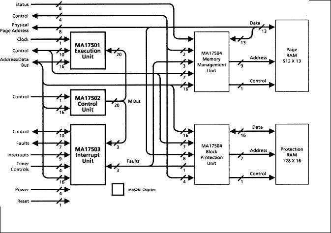
The MA17501 Execution Unit is a component of the Dynex BLOCK DIAGRAM Semiconductor MAS281 chip set. Other chips in the set
include the MA17502 Control Unit and the MA17503 lnterrupt Unit. Also available is the peripheral MA31751 Memory Management Unit/Block Protection Unit. These chips in conjunction implement the full MlL-STD-1750A lnstruction Set.
The MA17501 - consisting of a full function 16-bit ALU, 24 x 16-bit dual-port RAM register file, 32-bit barrel shifter, 4 x 24bit parallel multiplier, synchronisation clock generation logic, and microcode decode logic - provides all computational, logical, and synchronisation functions for the chip set. Table 1 provides brief signal definitions.
The MA17501 is offered in several package styles including; dual-in-line, flatpack and leadless chip carrier. Full packaging information is given at the end of the document.
FEATURES
■MIL-STD-1750A Instruction Set Architecture
■Full Performance over Military Temperature Range (-55°C to +125°C)
■Radiation Hard CMOS/SOS Technology
■16-Bit Bidirectional Address/Data Bus
■16-Bit Full Function Registered ALU
■32-Bit Barrel Shifter
■24 x 16-Bit Dual-Port RAM File
•16 User Accessible General Purpose Registers
•8 Microcode Accessible Registers
■4 x 24-Bit Parallel Multiplier
•48-Bit Accumulator
•16-Bit x 16-Bit Multiply in 4 Machine Cycles
■Instruction Pre-Fetch
■MAS281 Integrated Built-in Self Test
■TTL Compatible System Interface
1.0 SYSTEM CONSIDERATIONS
The MA17501 Execution Unit (EU) is a component of the Dynex Semiconductor MAS281 chip set. This chip set implements the full MlL-STD-1750A instruction set architecture. The other chips in the set are the MA17502 Control Unit (CU) and the MA17503 Interrupt Unit (IU). Also available is the peripheral MA31751 Memory Management Unit/Block Protection Unit (MMU(BPU)).
Figure 1 depicts the relationship between the chip set components. The EU provides the arithmetic and logical computation resources for the chip set. The EU also provides program sequencing logic in support of branching and subroutine functions. The lU provides interrupt and fault handling resources, DMA interface control signals, and the three MIL-STD-1750A timers. The EU and lU are each controlled by microcode from the CU. The MMU(BPU) may be configured to provide 1M-word memory management (MMU) and/or 1K-word memory block write protection (BPU) functions.
1/35
MA17501
Figure 1: MAS281 Chip Set with Optional MA17504 and Support RAMs
As shown in Figure 1, the MAS281 is the minimum processor configuration consisting of an Execution Unit, a Control Unit, and an Interrupt Unit. This configuration is capable of accessing a 64K-word address space. Addition of a MA31751 allows access to a 1M-word address space and/or provides hardware support for 1K-word memory block write protection.
The EU, as with all components of the MAS281 chip set, is fabricated with GEC Plessey Semiconductors CMOS/SOS process technology. lnput and output buffers associated with signals external to the MAS281 are TTL compatible.
Detailed descriptions of the EU's companion chips are provided in separate data sheets. Additional discussions on chip set system considerations, interconnection details, and DAlS mix benchmarking analysis are provided in separate applications notes.
The Execution Unit consists of a full function 16-bit ALU, 32-bit barrel shifter, 4 x 24-bit parallel multiplier, 24 x 16bit dual-port RAM register file, processor status word register, three operand transfer registers, three instruction fetch registers, various interconnect buses, synchronization clock generation logic, and microcode decode logic. Details of these components are depicted in Figure 2 and are discussed below:
2.0ARCHITECTURE
2.1ALU
The ALU is a full function 16-bit arithmetic/logic unit capable of performing arithmetic and logic operations on either one or two 16-bit operands in a single machine cycle. ln addition to operand manipulation, the ALU is used to compute memory addresses.
The ALU supports 16-bit fixed-point single-precision, 32-bit fixed-point double-precision, 32-bit floating-point, and 48-bit floating-point extended-precision data in two’s complement representation. Double-precision and extended-precision operands are passed through the ALU 16 bits at a time on consecutive machine cycles. Machine flags provide an indication of ALU results and are used to set condition status (CS) bits C, P, Z, and N in the Status Word Register. Condition status bits and the Status Word register are discussed below.
2/35
MA17501
|
Signal |
I/O |
Definition |
|||||||||||||||||||
|
|
|
|
|
|
|
|
|
|
|
|
|
|
|
|
|
|
|
|
|
|
|
|
AD00 - AD15 |
I/O |
External 16-Bit Address/Data Bus |
|||||||||||||||||||
|
AS |
O/Z |
Address Strobe Indicates Address lnformation on A/D Bus |
|||||||||||||||||||
|
CLKPC |
|
|
|
|
O |
Precharge Clock |
|||||||||||||||
|
CLK02 |
|
|
|
|
O |
Phase 2 Clock |
|||||||||||||||
|
PAUSE |
|
|
|
l |
DMA Acknowledge (A/D Bus to be used for DMA) |
||||||||||||||||
|
DS |
|
|
|
|
|
|
|
|
|
|
|
|
|
|
O/Z |
Data Strobe lndicates Data lnformation on A/D Bus |
|||||
|
HLDAK |
|
|
|
O |
Hold Acknowledge |
||||||||||||||||
|
HOLD |
|
|
|
|
l |
Hold Request Suspends lnternal Processor Functions |
|||||||||||||||
|
lN/ |
OP |
|
|
|
|
|
O/Z |
lnstruction/Operand lndicates Type of Memory Access |
|||||||||||||
|
INTRE |
|
|
|
O |
lnterrupt Enable |
||||||||||||||||
|
lRDY |
|
|
|
|
|
l |
lnterrupt Unit Ready Signal |
||||||||||||||
|
M/ |
lO |
|
|
|
|
|
|
O/Z |
Memory or lnput/Output lndicates Transaction on A/D Bus |
||||||||||||
|
M00 - M19 |
l |
20-Bit Microcode Bus |
|||||||||||||||||||
|
OSC |
l |
External Oscillator Clock |
|||||||||||||||||||
|
|
|
|
|
|
|
|
|
|
O |
Overflow lndicator |
|||||||||||
|
OVl |
|||||||||||||||||||||
|
PlF |
|
|
|
|
|
|
l |
Privileged Instruction Fault |
|||||||||||||
|
RD |
|
|
|
|
|
|
O/Z |
Read/Write IndicatesData Direction on A/D Bus |
|||||||||||||
|
/W |
|||||||||||||||||||||
|
|
|
|
|
|
l |
Ready lnforms CPU of the Conclusion of External Bus Cycle |
|||||||||||||||
|
RDY |
|||||||||||||||||||||
|
RESET |
l |
Reset Indicates Device Initialization |
|||||||||||||||||||
|
SYNCLK |
|
|
O |
Interrupt Unit's Sync Clock |
|||||||||||||||||
|
SYNC |
|
|
O |
System Clock - CPU Sync Clock (External) |
|||||||||||||||||
|
SYSCLK1 |
|
O |
System Clock (Internal) |
||||||||||||||||||
|
TEST |
|
I |
Test Enable |
||||||||||||||||||
|
T1 |
O |
Branch or Jump Control |
|||||||||||||||||||
|
VDD |
|
Power (External), 5 Volts |
|||||||||||||||||||
|
GND |
|
Ground |
|||||||||||||||||||
|
|
|
|
|
|
|
|
|
|
|
|
|
|
|
|
|
|
|
|
|
|
|
Table 1: Signal Definitions
2.2BARREL SHIFTER
The Barrel Shifter is a 32-bit input, 16-bit output right shift
network. A 32-bit operand may be shifted right arithmetically, logically, or cyclically up to 31 bit positions in a single machine cycle. While not directly accessible or visible to user programs, the Barrel Shifter is utilized by microcode to effect all shift, rotate, and normalize instructions with minimum execution time.
2.3 PARALLEL MULTIPLIER
The Parallel Multiplier performs a 4-bit multiplier by 24-bit multiplicand multiplication plus accumulation in a single machine cycle. Only four machine cycles are required to complete a 16-bit by 16-bit multiplication. Contained within the multiplier is a 48-bit product accumulation register with the lower 24 bits serving as a source operand register.
On each multiply machine cycle, the lower four bits of the accumulator are multiplied by 24 bits from the two ALU operand source buses (R and S). The lower 24 bits of this 28bit product are then added to the upper 24 bits of the accumulator and the whole accumulator is shifted right four bits. This right shift makes room for the upper four bits of the product. The four bits shifted out are used in the next multiply iteration.
2.4DUAL-PORT REGISTER FILE
The Register File is a dual port RAM structure containing
24, 16-bit registers. Sixteen of these registers are general purpose and user accessible. These user accessible registers - referred to as R0 through R15 - may be used as accumulators, index registers, base registers temporary operand registers, or stack pointers. The remaining eight registers are only accessible by microcode.
Adjacent registers are concatenated to effectively form 32bit and 48-bit registers for storage of double precision and extended-precision operands, respectively. Instructions access these operands by specifying the register containing the most significant part of the operand, and the register set wraps around automatically under microcode control, e.g., R15 concatenates with R0 for 32-bit operands and R15 concatenates with R0 and R1 for 48-bit operands.
3/35

MA17501
Figure 2: MA17501 Execution Unit Architecture
2.5 STATUS WORD REGISTER
The Status Word Register (SW) holds the condition status (CS) bits C, P, Z, and N generated by ALU operations. The SW also stores the address state (AS) and processor state (PS) fields. Figure 3 defines the Status Word Register storage format. The CS bits are stored with each logical, shift, and arithmetic operation performed by the ALU as required by MlL- STD-1750A and remain valid until changed by subsequent operations. The CS bits are interrogated during "jump on condition" and "instruction counter relative" MlL-STD-1750A branch instructions.
2.6 OPERAND TRANSFER REGISTERS
The Address (A), Data Output (DO), and Data lnput (Dl) registers are referred to as Operand Transfer Registers. These registers serve as storage buffers between internal EU buses and the EU's externally accessible address/data (AD) Bus. The DO register buffers data transferred from the EU to the AD Bus. The A register buffers operand addresses and XlO commands onto the AD Bus. The Dl register buffers data transferred from the AD Bus to the EU .
4/35
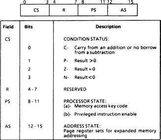
Figure 3: Status Word Format
2.7 INSTRUCTION FETCH REGISTERS
The Instruction Counter (IC), Instruction A (IA), and Instruction B (IB) registers allow sequential instruction fetches to be performed without assistance from the ALU. The lC register, which holds the 16-bit address of the next instruction to be fetched from memory, is loaded automatically by reset, jump, or branch operations. Once loaded, it functions as a dedicated counter to sequence from one instruction to the next. The current IC contents may be stored in registers R0 through R15 or in memory (pushed onto a stack) to provide return linkages for subroutine calls. As part of the microcoded interrupt handling routine the lC is saved in memory via the interrupt linkage pointer.
Registers lA and IB provide an instruction look-ahead capability. ln the case of 16-bit instructions, lB holds the instruction currently executing while lA holds the next instruction to be executed. ln the case of 32-bit instructions, IB and lA each hold half of the instruction. IA and Dl (Dl stores the immediate operands) are loaded as the instruction in lA is transferred to lB for execution; if the instruction in lB uses an immediate operand, lA is reloaded with the next instruction while Dl maintains the immediate data. This overlapping of operations allows higher performance levels to be achieved.
2.8BUSES
Three 16-bit wide buses (R, S, and Y) interconnect the EU
data storage and computational elements. The R and S buses accept operands from selected EU data storage elements and route them to inputs of selected EU computational elements. The Y, or destination, bus serves to route computational results either back to EU data storage and computational elements or to the various operand transfer registers.
A 16-bit multiplexed Address/Data (AD) Bus provides a communications path between the EU, other components of the MAS281 chip set, and any other devices mapped into the chip set's address space. Data transfers between the AD Bus and the R, S, and Y buses are buffered by the operand transfer registers.
MA17501
A 20-bit multiplexed microcode (M) bus provides a pathway between the Control Unit (CU) and the Execution Register (E) buffered microcode decode logic on the EU chip. Microcode placed on this bus by the CU controls all actions of the EU.
2.9SYNCHRONISATION CLOCK GENERATION LOGIC
The Execution Unit generates all of the synchronisation
clocks required by the chip set and CPU system. The EU converts an externally supplied oscillator signal into five synchronisation signals: SYNCN, SYSCLK1N,SYNCLKN, CLKPCN, CLK02N. The EU generates SYNCN for elements external to the chip set whereas SYNCLKN and SYSCLK1N are generated for the Interrupt Unit and internal EU synchronisation, respectively. SYSCLK1N is also brought out on a pin for use by external monitoring systems. The EU generates CLKPCN and CLK02N for use in the Control Unit. The CU uses CLKPCN to precharge the M Bus and transmit the first microword while CLK02N is used to transmit microword two.
The EU also contains the wait state generation interface. Failure of memory or l/O subsystems to drive RDYN low at the proper time during the DSN pulse causes the EU to hold SYNCLKN, SYNCN, SYSCLK1N, and CLKPCN in the high state; CLK02N, AS and DSN, in the low state; and RD/WN, IN/ OPN and M/ION in their current states for one or more oscillator cycles beyond the end of the normal five OSC cycle machine cycle. When RDYN is asserted low, the EU allows the machine cycle to conclude at the high-to-low transition of the current oscillator cycle. This will allow all the synchronisation and control signals to resume normal operation.
Additionally, IRDYN is used to signal completion of internal l/O command control of the lnterrupt Unit (IU). The IU thus can extend the duration of the above mentioned bus signals. Failure of the lU to drive lRDYN low at the proper time during the DSN low pulse causes the EU to hold SYNCLKN, SYNCN, SYSCLK1N, and CLKPCN in the high state; CLK02N, AS, and DSN in the low state; and lN/OPN, M/lON, and RD/WN in the state for the normal five OSC cycle machine cycle. When the lU asserts IRDYN low, the EU allows the machine cycle to conclude at the high-to-low transition of the current oscillator cycle. This will allow all the synchronisation and control signals to resume normal operation.
[NOTE: Whenever the EU is executing a machine cycle which requires IRDYN to drop low for completion, the machine cycle will be a minimum of six OSC cycles long. The maximum duration of this machine cycle depends on the length of time that the lU holds IRDYN high.]
5/35
MA17501
3.0 INTERFACE SIGNALS
All signals comply with the voltage levels of Table 1. ln addition, each of these functions is provided with Electrostatic Discharge (ESD) protection diodes. All unused inputs must be held to their inactive state via a connection to VDD or GND. A 500-ohm pull-up at the OSC input pin is recommended to damp line reflections.
Throughout this data sheet, active low signals are denoted by either a bar over the signal name or by following the name with an "N" suffix, e.g., HOLDN. Referenced signals that are not found on the MA17501 are preceded by the originating chip's functional acronym in parentheses, e.g., (lU)DMARN.
A description of each pin function, grouped according to functional interface, follows. The function acronym is presented first, followed by its definition, its type, and its detailed description. Function type is either input, output, high impedance (Hi-z), or a combination thereof. Timing characteristics of each of the functions described is provided in Section 5.0.
3.1POWER INTERFACE
The power interface consists of one 5V VDD connection
and three common GND pins.
3.2 CLOCKS
The Execution Unit provides the synchronisation clocks for the MAS281 chip set. Together these clocks form the basic operation cycle.
3.2.1 Oscillator (OSC)
lnput. The MA17501 requires a single external oscillator input for operation. The EU converts the oscillator into the five other clocks listed in this section. To minimise skew between OSC edges and signals derived from OSC, the OSC rise and fall times should be minimised. lt is recommended that a clock driver with high drive capability, such as a 54AS244, 54ALS244 or 54HST240, be used to drive the OSC input.
ln order to avoid double clocking due to line reflections, a 500-ohm pull-up resistor, placed close to the EU, is recommended.
3.2.2 Synchronisation Clock (SYNCN)
Output. The MA17501 provides the MAS281 Synchronisation Clock output to synchronise external circuitry to the MAS281 machine cycle. The high-to-low transition of this signal indicates the start of a new machine cycle.
SYNCN cycles associated with external memory or l/O bus transactions are a minimum of five OSC cycles in duration and may be extended by inserting wait states via the RDYN input. SYNCN low indicates that either an address or XlO command is on the AD Bus; a high indicates data is on the bus. Wait states extend the high state of SYNCN.
SYNCN cycles associated with internal CPU operations are either five or six OSC cycles in duration. Six OSC cycles are required for machine cycles associated with microcode branches or with the execution of internally (Interrupt Unit) decoded XlO commands. Five OSC cycles are used for all other internal operations, e.g., register to register transfers, ALU functions, etc.
[NOTE: For MAS281s operating at high OSC frequencies, the lnterrupt Unit logic that creates lRDYN may cause a wait state to be inserted during execution of internal XlO commands. This would result in a SYNCN cycle of seven OSC cycles duration. Though unlikely, this condition must be taken into account in implementing a RDYN generation circuit. Refer to the description of the RDYN signal for further details].
3.2.3 IU Synchronisation Clock (SYNCLKN)
Output. The SYNCLKN signal is a logical equivalent of the SYNCN signal provided for Interrupt Unit synchronisation.
3.2.4 System Clock (SYSCLK1N)
Output. SYSCLK1N is the MA17501's synchronization clock. It is the logical equivalent of SYNCN and SYNCLKN with the exception that during PAUSEN low or during HLDAKN low, SYSCLK1N is held in its low state. SYSCLK1N, like SYNCLKN, has a VSS to VDD logic level swing.
3.2.5 Precharge Clock (CLKPCN)
Output. CLKPCN is used by the MA17502 Control Unit (CU) to synchronize the precharging of the internal M Bus and most other CU operations to the MAS281 machine cycle.
CLKPCN cycles associated with MAS281 external memory or l/O bus transactions are a minimum of five OSC cycles in duration and are extended when wait states are inserted via the RDYN input. CLKPCN low indicates that the internal CU M Bus is being precharged to the high state; the low-to-high transition places the lower 20 bits of a microinstruction on the external M Bus. Wait states extend the high state of CLKPCN. When PAUSEN or HLDAKN is low, CLKPCN is held low.
CLKPCN cycles associated with internal MAS281 operations are either five or six OSC cycles in duration. Six OSC cycles are required for machine cycles associated with microcode branches or with the execution of internally (lnterrupt Unit) decoded XlO commands. Five OSC cycles are used for all other internal operations, e.g., register to register transfers, ALU functions, etc.
[NOTE: For MAS281s operating at high OSC frequencies, the lnterrupt Unit logic that creates lRDYN may cause a wait state to be inserted during execution of internal XlO commands. This would result in a CLKPCN cycle of seven OSC cycles duration.]
6/35
MA17501
3.2.6 Phase 2 Clock (CLK02N)
Output. CLK02N is used by the MA17502 Control Unit (CU) in conjunction with CLKPCN to synchronize microinstruction transmission on the M Bus to the MAS281 machine cycle.
CLK02N cycles associated with MAS281 external memory or l/O bus transactions are a minimum of five OSC cycles in duration and are extended when wait states are inserted via the RDYN input.
The high-to-low transition of CLK02N places the upper 20 bits of a microinstruction on the external M Bus. Wait states extend the trailing (based on SYNCN high-to- low beginning the machine cycle) low state of CLK02N. When PAUSEN or HLDAKN is low, CLK02N is held high.
CLK02N cycles associated with internal MAS281 operations are either five or six OSC cycles in duration. Six OSC cycles are required for machine cycles associated with microcode branches or with the execution of internally (Interrupt Unit) decoded XlO commands. Five OSC cycles are used for all other internal operations, e.g., register to register transfers, ALU functions, etc.
[NOTE: For MAS281s operating at high OSC frequencies, the Interrupt Unit logic that creates IRDYN may cause a wait state to be inserted during execution of internal XlO commands. This would result in a CLK02N cycle of seven OSC cycles duration.]
3.3 BUS CONTROL
This group of signals is provided to control Address/ Data (AD) bus transmissions (See Figure 4). The signals indicate when address or data information is on the AD Bus and what type of transaction is taking place during a particular machine cycle.
3.3.1 Address Strobe (AS)
Output/Hi-z. AS high indicates that the Address/Data (AD) Bus contains address information. The address information is assured stable at the high-to-low transition
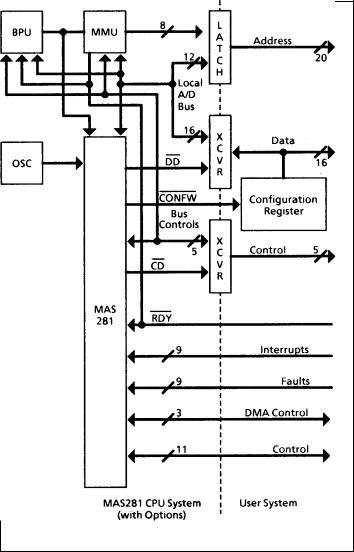
of this signal. ln this way, AS provides the necessary Figure 4: Typical MAS281/MA17504 System Interface control for a system Address Bus transparent latch
system interface.
The Interrupt Unit uses AS to extract the XlO command information off the AD Bus for internally decoded XlO commands, and the Memory Management Unit/Block Protection Unit (MMU(BPU)) uses AS to extract address information for memory management and block protection functions, and to extract XlO command information for MMU(BPU) decoded XlO commands.
AS is placed in the high-impedance state during DMA cycles by PAUSEN low and during the Hold state by HLDAKN low. During internal non-AD Bus related CPU operations, AS is held low for the entire machine cycle via microcode control.
7/35
MA17501
3.3.2 Data Strobe (DSN)
Output/Hi-z. DSN low indicates that data is on the AD Bus (write/output cycles) or that the MAS281 AD Bus drivers are in the high-impedance state (read/input cycles). For write/output cycles, the data is guaranteed stable at the low-to-high transition of DSN. For read/input cycles, the DSN low-to-high transition indicates the acceptance of data by the MAS281 (SYSCLK1N high-to-low transition latches AD Bus data into the lA and Dl registers).
DSN is placed in the high-impedance state during DMA cycles by PAUSEN low and during the Hold state by HLDAKN low. DSN is held high, for the entire machine cycle, during internal non-AD Bus operations via microcode.
3.3.3 Read/Write (RD/WN)
Output/Hi-z. RD/WN defines the direction of data flow on the bidirectional AD Bus and provides read/write cycle information to the MMU(BPU) for write protection control. RD/WN high indicates a read/input bus cycle and data transfer to the MAS281. RD/WN low indicates a write/output bus cycle and data transfer from the MAS281.
This signal is asserted at the SYNCN high-to-low transition and remains valid for the duration of the current SYNCN period. RD/WN is placed in the high impedance state during DMA cycles by PAUSEN low and during the Hold state by HLDAKN low.
3.3.4 Memory/lnput-Output (M/ION)
Output/Hi-z. M/lON defines the type of device involved in the data transfer occurring on the AD Bus and provides functional control for the lnterrupt Unit (lU) and the Memory Management Unit/Block Protection Unit (MMU(BPU)). The lU ignores memory transfer AD Bus activity and the MMU(BPU) uses M/lON to decide whether to decode the address information on the AD Bus as an MMU(BPU) XlO command or a memory address. M/lON high indicates a memory access, and M/lON low indicates an input-output operation.
This signal is asserted at the SYNCN high-to-low transition and remains valid for the duration of the current SYNCN period. M/lON is placed in the high impedance state during DMA cycles by PAUSEN low and during the Hold state by HLDAKN low. M/lON is raised high, for the entire machine cycle, during internal non AD Bus operations via microcode.
3.3.5 Instruction/Operand (IN/OPN)
Output/Hi-z. lN/OPN high indicates an instruction is to be read from memory during the current AD Bus cycle. IN/OPN is low for all other MAS281 directed AD Bus transfers. The Memory Management Unit/Block Protection Unit (MMU(BPU)), when configured as a MMU, uses lN/OPN to select the proper page register set within the specified page register group.
IN/OPN is asserted at the SYNCN high-to-low transition and remains valid for the duration of the current SYNCN period. lN/OPN is placed in the high-impedance state during DMA cycles by PAUSEN low and during the Hold state by HLDAKN low.
3.3.6 Ready (RDYN)
Input. During external AD Bus transfers (those dealing with devices external to the MAS281 chip set), a low is required on this input to allow the MAS281 machine cycle to complete (high-to-low transition of SYNCN). RDYN high is used to prolong the data portion of the machine cycle (SYNCN high) to accommodate slow memory and l/O devices. The MAS281 assumes memory or l/O devices are NOT ready to provide (accept) data to (from) the AD Bus, and requires these devices to signal their readiness via the RDYN input.
A low on RDYN, enveloping the current machine cycle's fifth (or later) OSC cycle high-to-low transition, allows the current machine cycle to complete (SYNCN high-to-low transition) at the following low-to-high transition of the OSC input.
3.4 BUSES
The following is a discussion of the communication buses connecting the MA17501 to the other chips of the MAS281 set. The AD Bus transfers all data and instructions and the M Bus provides the microcode instructions from the MA17502.
3.4.1 Address/Data Bus (AD Bus)
Input/Output/Hi-z. These signals comprise a 16-bit bidirectional multiplexed address and data bus. During external bus transfers, the AD Bus accommodates the transfer of address and data information between the MA17501 and memory, or l/O ports. During internal bus operations, the AD Bus provides additional communication among the Execution, Control, Interrupt and Memory Management/Block Protection Units. AD00 is the most significant bit position and AD15 is the least significant bit position of both the 16-bit data and 16-bit address. A high on this bus corresponds to a logic one and a low corresponds to a logic zero.
Address information is valid on the bus at the AS high tolow transition. The RD/WN signal indicates the MA17501 AD Bus drivers state during the data portion of the bus cycle (DSN low) and the M/lON function defines the type of device the transfer is with. The AD Bus drivers are placed in the high impedance state during Read operations (DSN low), during DMA cycles by PAUSEN low, and during the Hold state by HLDAKN low.
8/35
3.4.2 Microcontrol Bus (M Bus)
Input. The M Bus is a 20-bit multiplexed microcontrol bus which provides microcoded control to the EU. The Control Unit multiplexes the 40-bit microcode instructions into two 20-bit words. The upper 20 bits are placed on the M Bus by the CLKPCN low-to-high transition and the lower 20 bits are placed on the M Bus by the trailing high-to-low transition of CLK02N. The microinstruction is reassembled in the EU’s Execution (E) register and used to control EU functions during the next machine cycle. M19 is the most significant bit position and M00 is the least significant bit position for both microwords. The high order 20 bits are transmitted first, followed by the low order 20 bits of the microinstruction. A high on this bus corresponds to a logic one and low corresponds to a logic zero.
3.5SYSTEM SUPPORT INTERFACE
The system support interface signals have control over
functions that affect the chip set as a whole.
3.5.1 Processor Pause (PAUSEN)
lnput. PAUSEN is driven low by the lnterrupt Unit upon acknowledgement of a DMA transfer request. A low on PAUSEN causes the EU to place all the bus control signals (AS, DSN, M/lON, RD/WN, IN/OPN) and the AD Bus in the high impedance state, and to disable all clock outputs, except for SYNCLKN and SYNCN. The requesting device maintains control of the AD Bus and bus control lines until (lU)DMARN is raised high, thus causing PAUSEN to raise high.
lt is recommended that the MAS281 chip set be buffered to the memory/input-output system. lf an MMU(BPU) peripheral chip is used for memory expansion/protection it must reside on the MAS281 side of these buffer transceivers (see Figure 4). Thus, for a DMA device to access the MMU(BPU), the MAS281 AD Bus and bus control signal drivers must be in the high impedance state to allow the DMA device to drive these signals. The interrupt Unit also provides the CDN signal for the directional control of the bus control transceivers.
3.5.2 Processor Hold Request (HOLDN)
lnput. A low on this input suspends all chip set functions (except SYNCN and SYNCLKN) at the end of the current MlL- STD-1750A instruction. The AD Bus and bus control functions (AS, DSN, M/ION, lN/OPN, RD/WN) are placed in the high impedance state permitting a monitor system to take control of the memory/input-output system. The internal synchronisation clocks are placed in an inactive state, which halts further instruction sequencing until HOLDN is released. As with DMA cycles, the reason for this is to allow access to the MMU(BPU) if an expanded memory system is used. The (lU)CDN output is provided for control bus transceiver directional control during the Hold state. This input should be synchronised to AS falling.
MA17501
3.5.3 Processor Hold Acknowledge (HLDAKN)
Output. HLDAKN drops low after reaching the end of the MIL-STD-1750A instruction during which HOLDN was pulled low, or after encountering a BPT software instruction. The Hold state is terminated by raising HOLDN high (if HOLDN low initiated the Hold state), or by pulsing HOLDN low (if the Hold state was initiated by a BPT instruction). During the Hold state, software execution is suspended and the MAS281 interface functions are placed in the high impedance state to allow a monitor system to take control of the memory/input-output system.
3.6INTER-CHIP CONTROL
The following signals perform control functions internal to
the MAS281 chip set. These functions include microcode execution branching control and arithmetic error indication.
3.6.1 Internal Ready (IRDYN)
Input. The IRDYN signal is the means by which Interrupt Unit (IU) command cycles, involving the AD Bus, are completed. The lU drops lRDYN low when the XlO command has been decoded and allows the six OSC period machine cycle to complete. The IRDYN and RDYN signals are effectively ORed together to control the EU clock generation circuitry; therefore, RDYN should be high during lU decoded XlO commands.
3.6.2 Interrupt Unit Microinstruction Enable (INTREN)
Output. The Execution Unit controls the lnterrupt Unit (lU) 3-bit microcode interface through the use of the INTREN signal. lNTREN low enables the lU microcode decoding logic. lU functions handled through microcode are; enable/disable DMA interface XlO command control, set Normal Power-Up discrete, load fault register, and read encoded 4-bit vector identifying the highest priority pending interrupt.
Machine cycles during lNTREN low are a special case of internal non-AD Bus operations. These cycles are denoted by a six OSC period machine cycle.
3.6.3 Overflow Indicator (OVIN)
Output. OVlN is an indication that a fixed-point overflow condition, as specified in MIL-STD-1750A, has occurred during an operation. The Interrupt Unit accepts this as an input to the pending interrupt register level four interrupt bit.
9/35
MA17501
3.6.4 Privileged Instruction Fault (PIFN)
lnput. PlFN low is an indication to the Execution Unit that a fault, requiring the current MlL-STD-1750A instruction to be aborted, has occurred. The faults that cause the instruction abort are 0, 5, and 8 which are, respectively, memory protect error ((IU)MPROEN low), an out-of-bounds memory/inputoutput address ((lU)EXADE low), or a bus fault timeout. ln response to PIFN low, the EU maintains AS low, DSN high, and forces the M/lON signal high for two machine cycles. ln addition, the EU will internally complete the current SYNCN cycle and resume operation. This allows the Control Unit to sequence to the interrupt handling routine without affecting the bus status.
3.6.5 Branch or Jump Control (T1)
Output. The Execution Unit raises the T1 signal high to indicate a microcode conditional branch condition is true. The Control Unit accepts T1 and feeds it into the microcode address multiplexer where microinstruction branches are effected.
3.6.6 Test Microword (TESTN)
lnput. The TESTN signal is used during chip test to load 40bit microinstructions into the EU execution register. TESTN low loads E39 (MSB) to E20, and TESTN high loads E19 to E00 (LSB). TESTN should be pulled-up to VDD in customer applications.
4.0 OPERATING MODES
The following discussions detail the MAS281 chip set operating modes from the perspective of the Execution Unit. MAS281 operating modes involving the MA17501 include: (1) Initialisation, (2) lnstruction Execution, (3) Interrupt Servicing,
(4) Fault Servicing, (5) DMA Support, and (6) Software Development Support.
4.1 INITIALISATION
RESET starts the chip set microcoded initialisation sequence, but also affects the Execution Unit Circuitry directly. When RESET is raised high, the Hold state acknowledge signal (HLDAKN) is forced high thus releasing the MAS281 from the Hold state (if changing HOLDN is unable to release the Hold state). RESET also forces the clock generation circuitry to create a five OSC period machine cycle by disabling state machine inputs that vary the machine cycle length.
Upon releasing RESET, the EU Hold State circuitry is enabled and the clock generation circuitry is allowed to function normally. HOLDN will not have an effect on chip set operation until the initialisation routine has completed because the microcode branch to the Hold routine is disabled.
The microcoded initialisation routine clears the lnstruction Counter (lC), Status Word Register (SW), and Register File (R00-R15) and performs the BlT. The successful completion of the BlT is necessary to guarantee the register file is cleared at the end of the initialisation routine.
The microcoded BIT exercises all legal microinstruction bit combinations and tests all internally accessible structures of the MAS281. For the Execution Unit this includes the full Register Set, ALU, Multiplier, Barrel Shifter, and Macroflag logic. Table 2 details the tests performed by each of the five BlT subroutines.
lf any part of BlT fails, an error code identifying the failed subroutine is loaded into the lnterrupt Unit Fault Register (via the AD Bus), BlT is aborted, and NPU is left in the low state. Table 2 defines the coding of the BlT results. (lNTREN enables microcode control of the lnterrupt Unit (lU) to raise NPU high (if BlT passes) and load BIT error codes (if BIT fails) into the lU Fault Register).
The last action performed by the initialisation routine is to load the instruction pipeline. Instruction fetches start at memory location zero (page zero) from the Start-Up ROM (if implemented). Whether or not BIT passes, the processor will begin instruction execution at this point.
[NOTE: To complete initialisation and pass BIT, interrupt and fault inputs must be high for the duration of the initialisation routine. Also, the Timers A and B must be clocked for BlT success.]
10/35
MA17501
BIT |
Test Coverage |
BIT Fail Codes (FT13,14,15) |
Cycles |
|
|
|
|
1 |
Mlcrocode Sequencer |
100 |
221 |
|
IB Register Control |
|
|
|
Barrel Shifter |
|
|
|
Byte Operations and Flags |
|
|
|
|
|
|
2 |
Temporary Registers (T0 - T7) |
101 |
166 |
|
Microcode Flags |
|
|
|
Multiply |
|
|
|
Divide |
|
|
|
|
|
|
3 |
Interrupt Unit - MK, Pl, FT |
111 |
214 |
|
Enable/Disable Interrupts |
|
|
|
|
|
|
4 |
Status Word Control |
110 |
154 |
|
User Flags |
|
|
|
General Registers (R0 - R15 |
|
|
|
|
|
|
5 |
Timer A |
111 |
763 |
|
Timer B |
|
|
|
|
|
|
- |
BIT Pass/Fail Overhead |
- |
26 |
|
|
|
|
Note: BIT pass is indicated by all zeros in FT bits 13, 14, and 15.
Table 2: MAS281 BIT Summary
4.2 INSTRUCTION EXECUTION
Instruction execution is characterised by a variety of operations composed of various types of machine cycles. The Execution Unit contains the clock generation circuitry that creates the different machine cycles depending on the particular operation being performed at the time. These operations include: (1) internal CPU cycles, (2) instruction fetches, (3) operand transfers, and (4) input/output transfers. Instruction execution may be interrupted at the end of any individual machine cycle by the PAUSEN (denoting DMA operations) clock generation circuitry input, and at the beginning of any given MIL-STD-1750A instruction by an (IU)IRN or HOLDN low input to the Control Unit.
4.2.1 Internal CPU Cycles
All CPU data manipulation and housekeeping operations are performed using internal CPU cycles. Internal CPU cycles are either five or six OSC periods long and are characterised by AS low and DSN, (IU)DDN, and M/ION high. Section 5.0 provides timing characteristics for internal CPU cycles.
The majority of lnternal CPU Cycles are five OSC period machine cycles. Six OSC period machine cycles occur when executing conditional jump or branch microinstructions; the EU is calculating the branch condition to determine the state of the T1 output signal.
4.2.2 Instruction Fetches
lnstruction fetches are used to keep the instruction pipeline full. This ensures that the next instruction is ready for execution when the preceding instruction is completed.
During jump and branch instruction execution the pipeline is flushed, then refilled via two consecutive instruction fetches starting at the new instruction location. The pipeline is also refilled as part of the interrupt and Hold processing.
lnstruction fetches are five (minimum) OSC period machine cycles characterised by IN/OPN, M/lON, and RD/WN high. lnstruction fetches use pipeline registers lA and IB, the instruction counter (lC), and the data input register (Dl). Assuming an empty instruction pipeline (as a result of a reset, jump or branch), the contents of lC are placed on the AD Bus as an address. The returned value (the instruction) is stored in the IA register. The lC register is incremented (dedicated counter mode) and the next fetch is performed.
This second returned value, which may be an instruction or an immediate operand, is stored in both the lA and Dl registers as the previous contents of IA advance to the IB register to be decoded into their microcoded routine. If the second returned value is an immediate operand, a third instruction fetch will occur with the instruction being loaded into lA only; Dl retains the immediate operand.
The data portion (SYNCN high) of instruction fetch cycles can be extended beyond their minimum five OSC periods by use of the RDYN signal. RDYN held high during the high-to- low transition of the machine cycles fifth OSC cycle will extend the data portion of the machine cycle. The machine cycle can be completed at any succeeding OSC cycle high-to-low transition by enveloping this OSC edge with RDYN low.
4.2.3 Operand Transfers
Operand transfers are used to obtain operands to be used by an instruction and to save any results of an instructions execution. Machine cycles associated with operand transfers are a minimum of five OSC periods in duration. The RDYN signal can be used to insert wait states into the data portion of the machine cycle (SYNCN high) to accommodate slow memory.
11/35
 Loading...