


DYNEX MAS28139ND, MAS28139NC, MAS28139NB, MAS28139FS, MAS28139FE Datasheet
...MA28139
OBDH Bus Terminal
Replaces June 1999 version, DS3592-5.0 |
DS3592-6.0 January 2000 |
The OBT ASIC will interface any user to the ESA On Board Data Handling bus. Developed under ESA Contract, it conforms to ESA OBDH, Digital Bus Interface and Internal User Bus Standards.
The OBT has 2 separate functions. The first is a 5 channel modem which, on the bus side, provides the digital waveforms necessary to operate the Litton Bus drivers, and receives the outputs of the Litton bus detectors. On the user side, it provides an input / output at Digital Bus Interface level. The second function, internally coupled to the first, provides a multiplexing / demultiplexing function of the DBI signals down to Internal User Bus levels and vectored 16 bit serial register read and write commands (see section 7.2 of ESA standard TTC-B-01). In effect, the second function of the OBT provides the core of an RTU.
The Interrogation and Response bus data streams of the two functions may be either coupled together (in RT mode) or isolated (in CT mode). The device may hence be used as a modem only, an RTU kernel only or as a combined modem and RTU kernel. In RT mode, the Interrogation bus data stream can be observed and the Response bus data from associated devices, such as an MA28138 Remote Bus Interface, can be combined with that from the RTU kernel before being used by the modem circuits to modulate the Response bus. Bi-directional access to the Block Transfer bus is provided in either mode.
When used to interface a central terminal to the OBDH bus, the OBT should be continuously clocked in order to output timing to all users on the I-bus as dummy interrogations from the CT. Commands and telemetry are normally sent on the I and BT busses whilst responses and telemetry normally return on the R and BT busses.
FEATURES
■Radiation Hard
■Low Power Consumption
■Single CMOS-SOS ASIC Implementation
■Latch-up Free
■High SEU Immunity
■Fully Compliant with ESA OBDH, IUB, DBI and RBI Specification
■Contains OBDH Bus Modem and RTU Kernel
■Supports Bi-directional Data Transfer on Response and Block Transfer Bus
|
|
|
CONFIGURATION PINS |
|
OBDH BUS |
|
|
|
|
I |
R BT |
|
|
|
|
I Rx |
|
|
INTERNAL |
|
|
|
USER |
|
|
|
|
RTU |
|
|
|
CLK DETECTOR, |
BUS |
|
|
R Rx |
WATCHDOG |
KERNEL |
|
|
I (CTU) |
|
|
|
|
R (RTU) Tx |
|
|
|
|
BT Rx |
CONTROL |
|
DIGITAL |
|
|
BUS |
||
|
|
LOGIC |
|
|
|
|
|
INTERFACE |
|
|
BT Rx |
|
|
|
|
|
|
|
|
|
|
CONTROL |
|
|
|
|
PINS |
|
|
Figure 1: Block Diagram
1/34
MA28139
APPLICATION
CENTRAL TERMINAL
Bus Controller
CT DBI
OBT
ODBH BUS |
|
|
|
|
UP TO A TOTAL OF 62 TERMINALS |
|
|
|
|
|
|||
|
|
|
|
|
|
|
|
|
|
|
|
|
|
OBT |
|
|
IUB |
DMUX |
MPX |
DMUX |
ADC |
Commands |
Digital |
Timing |
Data |
Address |
Analogue |
|
Data |
REMOTE TERMINAL |
|
OBT |
|
DBU |
|
RT |
DBI |
RBI |
|
RAM |
µP |
I/O |
|
OBT
RT DBI
|
RBI |
RAM |
µP |
|
I/O |
INTELLIGENT TERMINAL
Figure 2: Application
PAYLOAD INTERFACES
The OBT converts the OBDH bus to an Internal User Bus, and a Digital Bus Interface. The OBT can connect OBDH to existing ESA standard payload interfaces such as the MSS PIU (payload interface unit), ICU (intelligent control unit), SBC
(single board MIL-STD-1750 computer) or FTC (fault tolerant computer).
The OBT and analogue components/transformers can be integrated in the PIU, ICU, SBC, etc.
|
I-Bus |
|
IUB |
PAYLOAD |
|
|
|
|
PIU |
|
|
|
|
ANALOGUE |
OBDH |
|
|
|
R-Bus |
HYBRID |
BUS |
|
|
OBDH |
OR |
TERMINAL |
|
|
|
|
|
|
|||
|
|
DISCRETE |
MA28139 |
|
|
|
|
CIRCUIT |
|
|
|
|
|
|
|
μP |
|
|
BT-Bus |
|
DBI |
DMA |
|
|
|
|
RBI |
|
|
|
|
|
MA28138 |
AD-BUS |
|
|
|
|
|
PAYLOAD |
|
|
|
|
|
I/O |
|
|
|
|
|
|
|
|
|
|
SBC |
MEMORY |
|
|
|
|
|
|
Figure 3: Payload Interface
2/34
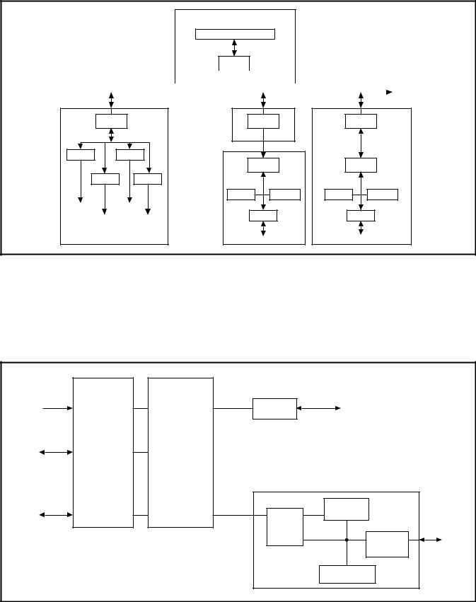
FUNCTIONAL DESCRIPTION
In RT mode, power up resets the OBT and causes it to deselect both busses. Two watchdog counters monitor the Nominal l-bus and the Redundant l-bus. If either bus becomes active, that bus will be selected. If the selected bus stops, the OBT watchdog times out and resets both the OBT and the user. If both busses become active, the Nominal bus will be selected in preference to the Redundant one. A change in bus selection will always result in the OBT and the user being reset. Responses from the user are always returned on the selected bus. Setting ‘SIMUL’ high causes both BATs to drive both the Nominal and the Redundant busses irrespective of the current bus selection. The time-out period may be set to any desired number of bits by varying the ‘LOSC’ frequency. The OBT derives all timing from, and is synchronous with, the selected l-bus. The OBT demodulates the l-bus to the DBI and decodes commands to the IUB.
The CTpRTn mode pin causes the modem circuits and the RTU Kernel to be either cascade or isolated. If CTpRTn is low (RT mode), the RIRSYNC, CLK, DATA and VAL signals are routed to the RTU Kernel and the associated pins act as
MA28139
outputs; responses from the RTU Kernel are ORed with those from the external RRTDATA and RRTEN inputs and can be independently monitored on the DATARRT and ENRRT pins. In this mode any reset caused by the Clock Detector watchdogs is also combined with the power up reset input.
If CTpRTn is high (CT mode), the modem and RTU Kernel functions are isolated to permit the device to be used as either a modem within the CTU or an RTU Kernel interfacing to an external modem where the RIRSYNC, CLK, DATA and VAL pins act as inputs. The right-hand multiplexer bank is switched to the upper position so that the CT drives the OBDH via the CIT and CBT (if used) pins and receives responses/telemetry via the CRR and CBR (if used) pins. Note: in CT mode, BAT1 must be connected to the l-busses.
In RT mode, the CITSEL, MOD, CLK, SYNC and INV pins are disabled and the clocks are supplied by the l-bus BAR in response to the selected bus. In CT mode, the Clock Detector is functional and drives the TlMEOUTn pin but is unable to cause internal reset on time-out; in this mode the CT must supply all clocks and select the operational bus.
The changes depending upon selection of RT mode or CT mode with the CTpRTn pin are defined in the table below:
Functional Signal |
CT Mode Source |
RT Mode Source |
|
(CTpRTn = ‘1’) |
(CTpRTn = ‘0’) |
|
|
|
BAT1, 2 modulation clock |
CITMOD input pin |
Recovered R2F |
|
|
|
BAT1, 2 data clock |
CITCLK input pin |
Recovered RIRCLK |
|
|
|
BAT1 data input |
RRTDATA input pin |
RRTDATA OR DATARRT (RTU Kernel) |
|
|
|
BAT1 tx enable |
‘1’ |
RRTEN OR DATAEN (RTU Kernel) |
BAT1 sync code tx enable |
CITSYNC input pin |
‘0’ |
BAT1 bit invalidate tx enable |
CITINV input Pin |
‘0’ |
BAT1, 2 bus selection |
CITSEL and SIMUL input pins |
Detected active bus and SIMUL input pin |
BAT2 data input |
RBTDATA input Pin |
RBTDATA input pin |
BAT2 tx enable |
RBTEN input pin |
RBTEN input pin |
BAT1, 2, BAR1, 2, 3 reset |
MRSTn input pin |
TlMEOUTn AND MRSTn input pin |
|
|
|
RIRSYNC, CLK, DATA, |
outputs |
inputs |
VAL pin direction |
|
|
BAT/BAR and RTU Kernel |
separated |
coupled |
coupling |
|
|
|
|
|
3/34

MA28139 |
|
|
|
|
|
|
|
|
|
|
|
|
OBDH |
|
|
|
|
|
|
|
|
|
|
|
|
NOMINAL |
REDUNDANT |
|
BUS |
|
|
|
|
|
|
|
|
|
BUS #1 |
BUS #2 |
LOSC |
TIME |
|
CT |
|
|
TAV |
|
|
|
|
I R BT |
I R BT |
OUT |
SIMUL |
MODE |
RESET |
TA0-5 |
|
|
|
|
||
|
|
|
|
|
|
|
|
|
|
|
||
|
|
CLOCK |
|
|
|
|
|
|
IUB |
|
|
|
|
|
DETECTOR |
|
|
|
|
RTU |
|
|
|
|
|
|
|
WATCHDOG |
|
BUS 1/2 |
|
KERNEL |
DATARRT |
|
|
|||
|
|
|
|
|
|
|
||||||
|
|
|
ACTIVE |
|
|
ENRRT |
|
|
||||
|
|
|
|
|
|
|
|
|
||||
|
|
|
|
|
|
|
|
|
|
|
||
|
NIDS1/2n, |
BAR1 |
|
|
OPEN |
|
SYNC, CLK, DATA, VAL |
RIR |
||||
|
RIDS1/2n |
|
|
|
|
|
|
|
||||
|
I-BUS RX |
|
|
|
|
|
|
|
|
|
||
|
|
|
|
|
CLK |
|
|
|
|
|
||
|
|
|
|
|
2F |
|
|
|
|
|
|
|
|
|
BAT1 |
|
|
|
|
|
SEL |
|
|
|
|
|
|
|
|
|
|
|
MOD |
|
|
|
||
|
|
|
|
|
|
|
|
|
|
|
|
|
|
|
|
|
|
|
|
|
|
CLK |
|
|
|
|
|
|
|
|
|
|
|
|
SYNC |
CIT |
|
|
|
|
|
|
|
|
|
|
|
|
|
|
|
|
|
|
|
|
|
0v |
|
|
|
|
|
|
|
|
R-BUS TX |
|
|
|
|
|
INV |
|
|
|
|
|
|
|
|
0v |
|
|
|
|
|
|
||
|
RR1-4, |
(RT MODE) |
|
|
|
|
|
|
|
|
||
|
|
|
|
|
|
DATA |
|
|
|
|||
|
|
|
|
|
|
|
|
|
|
|
||
|
NRE, RRE |
|
|
|
|
|
|
|
RRT |
|
|
|
|
|
|
|
|
|
|
|
|
|
|
||
|
|
I-BUS TX |
|
|
|
|
|
EN |
|
|
||
|
|
|
|
|
|
|
|
|
|
|||
|
|
(CT MODE) |
|
|
|
|
|
|
|
|
|
|
|
|
|
|
|
|
|
|
|
|
|
|
DBI |
|
|
BAR2 |
|
|
|
|
|
|
|
|
|
|
|
NRDS1/2n |
|
|
|
|
|
|
|
CLK, DATA, VAL |
RRR/CRR |
||
|
RRDS1/2n |
|
|
|
|
|
|
|
|
|
||
|
R-BUS RX |
|
|
|
|
|
INIT |
|
|
|
||
|
|
|
|
|
|
|
|
|
|
|||
|
|
BAT2 |
|
|
|
|
|
|
|
|
|
|
|
BR1-4, |
|
|
|
|
|
|
|
|
|
|
|
|
NBE, RBE |
|
|
|
|
|
|
|
|
|
|
|
|
|
BT-BUS TX |
|
|
|
|
|
DATA |
RBT/CBT |
|
||
|
|
|
|
|
|
|
|
|
EN |
|
|
|
|
|
BAR3 |
|
|
|
|
|
|
|
|
|
|
|
NBDS1/2n, |
|
|
|
|
|
|
|
CLK, DATA, VAL |
RBR/ |
||
|
RBDS1/2n |
|
|
|
|
|
|
|
||||
|
|
|
|
|
|
|
|
|
|
|||
|
|
BT-BUS RX |
|
|
|
|
|
INIT |
|
CBR |
|
|
|
|
|
|
|
|
|
|
|
|
|||
|
|
|
|
|
|
MA28139 OBT |
|
|
|
|
||
Figure 4: Architecture
Note: Switches in lower position - RT mode
Switches in upper position - CT mode
MODEM Modulation Waveforms are compliant with ESA document THB/Apo/KZ/1386/av. Waveforms indicating the operation of BAT1, 2 and BAR1, 2, 3 in both the CT and RT modes are shown in Figures 5 to 8.
4/34

Waveforms Transmitter Adaptor Bus Mode CT 5: Figure
Note 1: Raising CITSYNC for one bit period causes an invalid bit, a valid bit and another invalid bit to be modulated. The exact pattern is determined by RRTDATA; ‘110’ gives the classic H0H0H0L0L0L0 sync pattern.
Note 2: Valid Litton ‘1’ modulated. Note 3: Valid Litton ‘0’ modulated.
Note 4: Invalid Litton ‘0’ modulation is caused by raising CITINV for one bit period.
Note 5: Raising CITINV for more than one bit period only causes one invalid bit to be modulated. Note 6: BAT2 operation is similar, but SYNC and INV are not available.
5/34
MA28139

MA28139
Note: BAR2 and BAR3 operation are similar with different nomenclature.
Figure 6: RT Mode Bus Adaptor Transmitter Waveforms
6/34

Waveforms Receiver Adaptor Bus Mode RT 7: Figure
7/34
RIDS2n
Note 1: H0H0H0L0L0L0 sync pattern detected and resets phase of RIRCLK.
Note 2: Valid Litton ‘1’ detected.
Note 3: Valid Litton ‘0’ detected.
Note 4: Invalid Litton ‘0’ detected.
Note 5: Further invalid bits do not affect RIRVAL - it will rise as RIRSYNC rises.
Note 6: BAR2 and BAR3 operation is similar, but SYNC is not available and RRRINIT and RBRINIT are provided.
MA28139

8/34
Waveforms Receiver Adaptor Bus BAR2 8: Figure
MA28139
RIDS2n
Note 1: RRRINIT asynchronously resets RRRVAL to clear errors detected in the previous response.
Note 2: Valid Litton ‘1’ detected.
Note 3: Valid Litton ‘0’ detected.
Note 4: Invalid Litton ‘0’ detected.
Note 5: Further invalid bits do not affect RRRVAL - it will rise as RRRINIT rises.
Note 6: BAR3 operation is similar, but is intended to support Block Transfer - RBRINIT hence occurs once per block.
Note 7: Operation of BAR2 and BAR3 does not depend on RT mode or CT mode, except for bus selection.
MA28139
CLOCK DETECTOR OPERATION
The Clock Detector architecture is shown in Figure 9; a separate channel is essentially provided for each of the Nominal and Redundant Interrogation busses. Associated waveforms are shown in Figure 10.
Figure 9: Clock Detector Architecture
Each channel contains an Edge Detector and a 5-bit Watchdog Counter which respond only to high-to-low transitions on their respective Interrogation bus DS1n inputs. A common Bus Usage Detection circuit is used to generate timeout pulses (used for internal and external reset) and bus selection signals from the results of the watchdogs.
The local oscillator input, LOSC, is divided and decoded to generate an active low reset and an active high sample clock. When applied to both input Edge Detectors, these signals permit input high-to-low transitions to be detected for one LOSC cycle in every two (between the reset ↓ and sample clock −). Once such transitions have been detected by a sample clock, the associated watchdog counter is reset. The MSB of each watchdog counter is used as an indication of its bus’s status - active or inactive. Should the watchdog counter overflow (i.e. its MSB be set to 1), the associated bus will be considered inactive.
The status of the Nominal and Redundant Interrogation busses is used to determine internal bus selection for the modulation of Response and Block Transfer data in the device’s RT mode. If neither bus is considered active, the TlMEOUTn pin will be held low and RT mode reception of all 3 busses will be inhibited. If one bus is considered active, RT mode reception will occur on the same set of bus circuits (redundancy) as the active Interrogation bus. If both busses are considered active, RT mode reception from the Nominal set of bus circuits will be performed. RT mode transmission will always occur on the same set of bus circuits (redundancy) as selected for reception unless the SIMUL pin is held high, in which case transmission will occur simultaneously on both the Nominal and Redundant busses.
Both watchdog counters are fully set at power up to mark both busses as inactive - in this way, a missing LOSC input will not cause inactive busses to be deemed active.
For a single detected input transition, 17.5 to 18.5 LOSC cycles will elapse before the relevant bus is considered inactive. If near-instantaneous Nominal-to-Redundant or Dual- to-Redundant bus handover occurs, the change-over will be delayed by 18 to 19 LOSC cycles, in order to preserve the priority of the Nominal bus. If near-instantaneous Redundant- to-Nominal or Redundant-to-Dual bus handover occurs, the change-over will occur after 1.5 to 2.5 LOSC cycles since the Nominal bus takes priority. In either of these cases, a 1 LOSC cycle TlMEOUTn pulse is always generated to ensure that internal reset occurs.
The frequency of the local oscillator may be varied to make the nominal time-out period of 17.5 LOSC cycles correspond to any desired number of (missing) bits on the Interrogation bus. Variation of the duty cycle does not vary the time-out period. After 16 LOSC cycles without detected input transitions, the associated watchdog times-out and is detected on the next LOSC − edge; the generation of a TlMEOUTn pulse and reset are then inevitable.
For proper Clock Detector operation, (at least) one high-to- low input transition must be detected within a period of 16 LOSC cycles of the last such detection, but transitions made during alternate LOSC cycles (the phase is difficult to predict) will not be detected. Local oscillator clock signals which are harmonically-related to the modulation clock by an integer ratio are thus a cause for concern, although this problem is perhaps only likely to occur in experimental set-ups.
9/34

MA28139
Note: If both busses are determined by their watchdogs to be active (as indicated above by their status), the Nominal Bus will always be used by the Bus Adaptor Transmitter and Receiver circuits instead of the Redundant Bus.
Figure 10: MA28139 Clock Detector Operation
10/34
The requirement to respect set-up and hold times for the capture of the Edge Detector outputs by the LOSC high-to-low transition means that LOSC signals which are harmonicallyrelated to the Litton modulation clock but whose phase can not be controlled can never be guaranteed to provide reliable operation.
For asynchronous local oscillator signals, there will be no concern if we are simply able to place two or more Litton DSn high-to-low edges into each LOSC cycle, so that:
tMOD £ tLOSC - tSU - tHOLD
and the time-out period of 16 tLOSC is hence approximately 8 bit periods or more.
However, suppose that the periods of the modulation clock and the local oscillator clock are such that the relationship between them is:
tMOD = m tLOSC
where m is a positive integer.
In order to respect the setup and hold times, tSU + tHOLD respectively, between the DSn ¯, and LOSC ¯ edges, it is
necessary to avoid such harmonic relationships; it can be shown that around these spot frequencies it is necessary to ensure that either:
w tMOD ³ x tLOSC + tSU + tHOLD
or
y tMOD £ z tLOSC - tSU - tHOLD
where the integer constants w, x, y and z are given in the table below.
Since two modulation clock cycles occur per bit, the timeout period at these harmonics will then be:
16 tLOSC » 16 tMOD / m » 8 / m bit periods.
m |
w |
x |
y |
z |
Approx. time-out |
|
|
|
|
|
period (bit periods) |
|
|
|
|
|
|
1 |
15 |
15 |
17 |
17 |
8 |
2 |
7 |
15 |
8 |
15 |
4 |
3 |
5 |
15 |
5 |
15 |
2.67 |
4 |
3 |
13 |
4 |
15 |
2 |
5 |
3 |
15 |
3 |
15 |
1.6 |
6 |
2 |
13 |
2 |
11 |
1.33 |
7 |
1 |
7 |
1 |
7 |
1.14 |
8 |
1 |
9 |
2 |
15 |
1 |
9 |
1 |
9 |
1 |
9 |
0.88 |
10 |
1 |
11 |
1 |
9 |
0.8 |
11 |
1 |
11 |
1 |
11 |
0.73 |
12 |
1 |
13 |
1 |
11 |
0 67 |
13 |
1 |
13 |
1 |
13 |
0.62 |
14 |
1 |
15 |
1 |
13 |
0.57 |
15 |
1 |
15 |
1 |
15 |
0.53 |
|
|
|
|
|
|
MA28139
In summary, slow local oscillator clocks which cause relatively long timeout periods ³ 8 bit periods are not considered a problem; very long time-outs can be reliably implemented. For shorter time-out periods, however, it is necessary to avoid harmonic relationships between the Litton modulation clock and the local oscillator. The simplest practical method for avoiding such relationships would be to arrange for the ratio
n = tMOD / tLOSC
to have a half-integer value such that n = 0.5, 1.5, 2.5,
...using an independent crystal oscillator if necessary.
11/34
 Loading...