


DYNEX MAS28155LD, MAS28155LC, MAS28155LB, MAS28155CL, MAS28155CE Datasheet
...
MA28155
Radiation Hard Programmable
Peripheral Interface
Replaces June 1999 version, DS3575-4.0 |
DS3575-5.0 January 2000 |
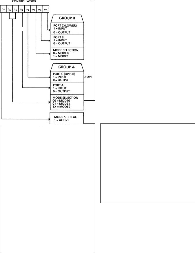
The MA28155 is a general purpose programmable Input/ Output device designed for use with the MAS281 microprocessor. It has 24 I/O pins which may be individually programmed in 2 groups of 12 and used in 3 major modes of operation.
In the first mode (MODE 0), each group of 12 I/O pins may be programmed in sets of 4 to be inputs or outputs. In the second mode (MODE 1), each group may be programmed to have 8 lines of input or output. Of the remaining 4 pins, 3 are used for hand-shaking and interrupt control signals. The third mode of operation (MODE 2) is the bidirectional bus mode, which uses 8 lines for a bidirectional bus and 5 lines, borrowing one from the other group, for hand-shaking.
FEATURES
■Radiation Hard to 1MRad (Si)
■High SEU Immunity, Latch Up Free
■Silicon-on-Sapphire Technology
■24 Programmable l/O Pins
■All Inputs and Outputs are TTL Compatible
■Direct Bit Set/Reset Capability Easing Control Application Interface
■Replaces Several MSI Packages
■Compatible with MAS281 (Mil-Std-1750A) Microprocessor
RD/WN
DSN
CSN
Figure 1: Block Diagram
1/20
MA28155
FUNCTIONAL DESCRIPTION
The MA28155 is a programmable peripheral interface (PPI) device designed for use with MAS281. Its function is that of a general purpose l/O component to interface peripheral equipment to the microcomputer system bus. The functional configuration of the MA28155 is programmed by the system software so that, normally, no external logic is necessary to interface peripheral devices or structures.
Data Bus Buffer
This 3-state, bidirectional, 8-bit buffer is used to interface the MA28155 to the system data bus. Data is transmitted or received by the buffer upon execution of input or output instructions by the CPU. Control words and status information are also transferred through the data bus buffer.
Read/Write and Control Logic
The function of this block is to manage all of the internal and external transfers of both Data and Control Status words. It accepts inputs from the CPU Address and Control busses and in turn, issues commands to both of the Control Groups.
Reset (RESET)
A high on this input clears the control register and all ports (A,B,C) are set to the input mode.
Chip Select (CSN)
A low on this input pin enables the communication between the MA28155 and the CPU.
Read/Write Select (RD/WN)
A high on RD/WN indicates a CPU read from the MA28155 and a low indicates a CPU data or control word write to the MA28155. The RD/WN line is active only when DSN is low.
Data Strobe (DSN)
This input indicates that a data transfer is taking place. During a CPU write operation the MA28155 reads data from the bus on the rising edge of DSN. During a read operation the MA28155 outputs data to the bus while DSN is low. Data is valid on the rising edge of DSN.
Port Select O and Port Select 1 (AO and A1 )
These input signals, in conjunction with the DSN and RD/ WN inputs, control the selection of one of the three ports of the control word registers. They are normally connected to the least significant bits of the address bus.
Basic Operation
A1 |
A0 |
DSN |
RD/WN |
CSN |
READ |
|
|
|
|
|
|
0 |
0 |
0 |
1 |
0 |
PORT A → DATA BUS |
0 |
1 |
0 |
1 |
0 |
PORT B → DATA BUS |
1 |
0 |
0 |
1 |
0 |
PORT C → DATA BUS |
|
|
|
|
|
WRITE |
|
|
|
|
|
|
0 |
0 |
0 |
0 |
0 |
DATA BUS → PORT A |
|
|
|
|
|
|
0 |
1 |
0 |
0 |
0 |
DATA BUS → PORT B |
|
|
|
|
|
|
1 |
0 |
0 |
0 |
1 |
DATA BUS → PORT C |
|
|
|
|
|
|
1 |
1 |
0 |
0 |
1 |
DATA BUS → CONTROL |
|
|
|
|
|
DISABLE |
|
|
|
|
|
|
x |
x |
x |
x |
1 |
DATA BUS → TRI-STATE |
|
|
|
|
|
|
1 |
1 |
0 |
1 |
0 |
ILLEGAL CONDITION |
|
|
|
|
|
|
x |
x |
1 |
x |
0 |
DATA BUS → TRI-STATE |
|
|
|
|
|
|
Table 1: Basic Operation
OPERATIONAL DESCRIPTION
Mode Selection
There are three basic modes of operation, which can be selected by the system software:
Mode 0. Basic Input/Output
Mode 1. Strobed Input/Output
Mode 2 Bi-directional Bus
When the reset input goes high all ports will be set to the input mode (i.e. all 24 lines will be in the high impedance state) After the reset is removed the MA28155 can remain in the input mode with no additional initialisation required.
During the execution of the system program any of the other modes may be selected using a single output instruction. This allows a single MA28155 to service a variety of peripheral devices with a single software maintenance routine.
The modes for Port A and Port B can be separately defined, while Port C is divided into two portions as required by the Port A and Port B definitions. All of the output registers, including the status register, will be reset whenever the mode is changed.
Modes may be combined so that their functional definition can be tailored to almost any l/O structure. For instance; Group B can be programmed in Mode 0 whilst Group A could be simultaneously programmed in Mode 1.
2/20
RD/WN, DSN |
A |
0 - A1, CSN |
|
|
|
C |
|
A |
A
A
Figure 2: Basic Mode Definitions and Bus Interface
Mode Definition Format (D7= 1)
MA28155
Single Bit Set/Reset Feature
Any of the eight bits of Port C can be Set or Reset using a single output instruction. This feature reduces software requirements in control-based applications.
When Port C is being used as Status/Control for Port A or B, these bits can be set or reset by using the Bit Set/Reset operation just as if they were data output ports.
Interrupt Control Functions
When the MA28155 is programmed to operate in Mode 1 or 2, control signals are provided that can be used as interrupt request inputs to the CPU (figure 4). The interrupt request signals, generated from Port C, can be inhibited or enabled by setting or resetting the associated INTE register bit, using the Bit Set/Reset function of Port C.
This function allows the programmer to disallow or allow a specific l/O device to interrupt the CPU, without affecting any other device in the interrupt structure.
INTE register bit definitions:
(BIT-SET): INTE is SET -Interrupt enable (BIT-RESET): INTE is RESET -Interrupt disable
Note: All mask register bits are automatically reset during mode selection and device reset.
Bit Set/Reset Format (D7 = 0)
BIT No.
S
E
L
B0
B1
B2
Figure 4: Bit Set/Reset Format (D7 = 0)
Figure 3: Mode Definition Format (D7 = 1)
3/20

MA28155
Group A and Group B Controls
The functional configuration of each port is programmed by the system software. In essence, the CPU outputs a control word to the MA28155. The control word contains information such as mode, bit set, bit reset, etc., this initializes the functional configuration of the MA28155.
Each of the Control blocks (Group A and Group B) accept commands from the Read/Write Control Logic, receive control words from the internal data bus and issue the proper commands to its associated ports:
Control Group A - Port A and Port C upper (C7-C4) Control Group B - Port B and Port C lower (C3-C0)
The Control Word Register can only be written into. Therefore reading of the Control Word Register is not allowed .
Ports A, B and C
The MA28155 contains three 8-bit ports (A, B, and C). All can be configured in a wide variety of functional characteristics by the system software but each has its own special features to further enhance the power and flexibility of the MA28155.
Port A.
One 8-bit data output latch/buffer and one 8-bit data input latch.
Port B.
One 8-bit data input/output latch/buffer and one 8-bit input buffer
Port C.
One 8-bit data output latch/buffer and one 8-bit data input buffer (no latch for input) This port can be divided into two 4-bit ports under the mode control. Each 4-bit port contains a 4-bit latch and it can be used for the control signal outputs and status signal inputs in conjunction with ports A and B
OPERATING MODE 0
(Basic Input/Output)
This functional configuration provides simple input and output operation for each of the three ports. No handshaking is required; data is simply written to or read from a specified port.
■Two 8-bit ports and 4-bit ports
■Any port can be input or output
■Outputs are latched
■Inputs are not latched.
■16 different Input/Output configurations are possible in this Mode.
DSN |
|
|
|
RD/WN set-up and hold time |
RD/WN
CSN, A1, A0
Figure 5: Basic Input (Read) Timing Diagram
4/20

MA28155
DSN
RD/WN set-up and hold time
RD/WN
CSN, A1, A0
Figure 6: Basic Input (Write) Timing Diagram
Port Definition Mode 0
D4 |
D3 |
D1 |
D0 |
PORT A |
PORT C |
PORT B |
PORT C |
|
|
|
|
(UPPER) |
|
|
(LOWER) |
|
|
|
|
|
|
|
|
0 |
0 |
0 |
0 |
OUTPUT |
OUTPUT |
OUTPUT |
OUTPUT |
|
|
|
|
|
|
|
|
0 |
0 |
0 |
1 |
OUTPUT |
OUTPUT |
OUTPUT |
INPUT |
|
|
|
|
|
|
|
|
0 |
0 |
1 |
0 |
OUTPUT |
OUTPUT |
INPUT |
OUTPUT |
|
|
|
|
|
|
|
|
0 |
0 |
1 |
1 |
OUTPUT |
OUTPUT |
INPUT |
INPUT |
|
|
|
|
|
|
|
|
0 |
1 |
0 |
0 |
OUTPUT |
INPUT |
OUTPUT |
OUTPUT |
|
|
|
|
|
|
|
|
0 |
1 |
0 |
1 |
OUTPUT |
INPUT |
OUTPUT |
INPUT |
|
|
|
|
|
|
|
|
0 |
1 |
1 |
0 |
OUTPUT |
INPUT |
INPUT |
OUTPUT |
|
|
|
|
|
|
|
|
0 |
1 |
1 |
1 |
OUTPUT |
INPUT |
INPUT |
INPUT |
|
|
|
|
|
|
|
|
1 |
0 |
0 |
0 |
INPUT |
OUTPUT |
OUTPUT |
OUTPUT |
|
|
|
|
|
|
|
|
1 |
0 |
0 |
1 |
INPUT |
OUTPUT |
OUTPUT |
INPUT |
|
|
|
|
|
|
|
|
1 |
0 |
1 |
0 |
INPUT |
OUTPUT |
INPUT |
OUTPUT |
|
|
|
|
|
|
|
|
1 |
0 |
1 |
1 |
INPUT |
OUTPUT |
INPUT |
INPUT |
1 |
1 |
0 |
0 |
INPUT |
INPUT |
OUTPUT |
OUTPUT |
|
|
|
|
|
|
|
|
1 |
1 |
0 |
1 |
INPUT |
INPUT |
OUTPUT |
INPUT |
|
|
|
|
|
|
|
|
1 |
1 |
1 |
0 |
INPUT |
INPUT |
INPUT |
OUTPUT |
|
|
|
|
|
|
|
|
1 |
1 |
1 |
1 |
INPUT |
INPUT |
INPUT |
INPUT |
|
|
|
|
|
|
|
|
Table 2: Port Definition Mode 0 (See Also Figure 3)
5/20
MA28155
OPERATING MODE 1
(Strobed Input/Output)
This functional configuration provides a means for transferring l/O data to or from a specified port in conjunction with strobes or handshaking signals. In mode 1, port A and port B use the lines on port C to generate or accept these handshaking signals
■Two Groups (Group A and Group B) .
■Each Group contains one 8-bit data port and one 4-bit control/data port,
■The 8-bit data port can be either input or output, Both inputs and outputs are latched,
■The 4-bit port is used for control and status of the 8-bit data port.
STBN
RD/WN
DSN
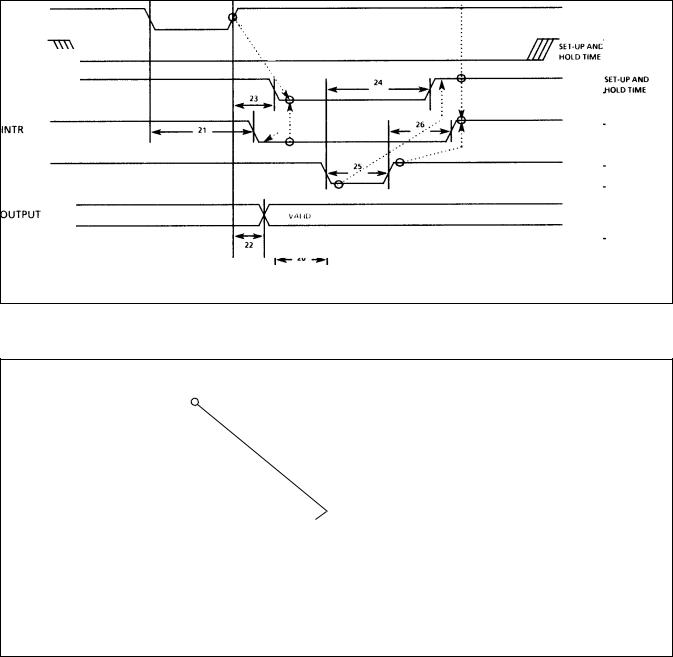
Figure 7: Strobed Input Timing Diagram
DSN
RD/WN
OBFN
ACKN
Figure 8: Strobed Output Timing Diagram
6/20
 Loading...