


MAS281
MIL-STD-1750A Microprocessor
Replaces June 1999 version, DS3563-4.0 |
DS3563-5.0 January 2000 |
The MAS281 Microprocessor is a MIL-STD-1750A (Notice BLOCK DIAGRAM 1), 16-bit Central Processing Unit (CPU). It consists of three
CMOS/SOS large-scale integration (LSI) chips: the MA17501 Execution Unit (EU), the MA17502 Control Unit (CU), and the MA17503 Interrupt Unit (IU). These three units can be mounted on, and interconnected within a 64-pin ceramic substrate. The microprocessor is also available as a 3-chip set without the ceramic substrate (see ordering information on page 55).
The MAS281 is optimised for real-time l/O and arithmetic intensive operations. Key performance-enhancing features include a parallel multiplier/accumulator, 32-bit barrel shifter, instruction pre-fetch queue, and multiport register file. Additional features include a comprehensive Built-ln-Test (BIT), interval timers A and B, trigger-go counter, and Start-Up ROM interface.
In accordance with MIL-STD-1750A, the MAS281 supports a 64K-word address space. An optional BMA31751 Memory Management Unit/Block Protect Unit (MMU(BPU)) chip may be added externally to expand this address space to 1M-words or add a 1K-word memory block protection capability,
The MAS281 is offered in several screening grades which are described in this document. For availability of speed grades, please contact Dynex Semiconductor.
FEATURES
■MIL-STD-1750A 16-Bit Microprocessor
■Full Performance over Military Temperature Range (-55°C to + 125°C)
■Radiation Hard CMOS/SOS Technology
■Performance Optimised Architecture
-Parallel Multiplier/Accumulator
-32-bit Barrel Shifter
-Instruction Pre-Fetch
-Multi-Port Register File
■Implements MlL-STD-1750AOptions
-Timers A and B
-Trigger-Go Counter
-Start-Up ROM Interface
■64 K-word Address Space Expandable to 1 M-word with Optional MMU
1/55

MAS281
1.0 ARCHITECTURE
The MAS281 Microprocessor is a high performance implementation of the MIL-STD-1750A (Notice 1) instruction set architecture. It consists of three custom CMOS/SOS Large Scale Integration chips referred to as the Execution Unit, Control Unit, and Interrupt Unit - mounted on, and interconnected within, a 64-pin, dual in-line ceramic substrate. Figure 1 depicts the interconnection of these chips via the substrate while Figure 2 depicts the architectural details within each chip.
Figure 1: MAS281 Microprocessor Block Diagram
Unit (MMU), this address space may be expanded to a full 1Mword. Furthermore, this configuration provides write and access lock and key protection down to 4K-word blocks. By also configuring the MA31751 as a Block Protect Unit (BPU), write protection may be extended down to 1K-word blocks. For those applications not requiring adherence to the address space requirements of MIL-STD-1750A, the MAS281 may be optionally configured with up to 1Mword each of instruction and operand space.
In addition to implementing all of the required features of MIL-STD-1750A, the MAS281 also incorporates a number of optional features. Interval timers A and B as well as a triggergo counter are provided. Most specified XIO commands are decoded directly on the module and an additional set of commands, associated with MMU and BPU operations, are directly decoded on the MA31751 chip. Those commands not directly decoded are output for decoding by external logic in accordance with the XIO and VIO protocols of MIL-STD- 1750A.
1.1 EXECUTION UNIT (EU)
The EU provides the computational resources for the MAS281. Key features include: (1) a three-bus (R, S, and Y) data path consisting of an arithmetic/logic unit (ALU), threeport register file, barrel shifter, parallel multiplier/accumulator, and status register; (2) instruction fetch registers IC, IA, and IB;
(3) operand transfer registers A, Dl, and DO; (4) a state sequencer; and (5) microinstruction decode logic. A brief description of these features follows:
1.1.1 ARITHMETIC/LOGIC UNIT (ALU)
A full function 16-bit ALU is used to perform arithmetic and logic operations on one or two 16-bit operands in a single machine cycle. The ALU supports 16-bit fixed-point singleprecision, 32-bit fixed-point double-precision, 32-bit floatingpoint, and 48-bit floating-point extended precision data in two’s complement form. The ALU generates several machine flags which reflect the outcome of its operations. These flags are stored in the condition status (CS) field of the status register.
1.1.2 THREE PORT REGISTER FILE
The MAS281 architecture has been optimised for both real time l/O and arithmetic intensive operations. Two key features of this architecture which contribute to the overall high performance of the MAS281 are; a barrel shifter and a parallel multiplier/accumulator. These subsystems allow the MAS281 to perform multi-bit shifts, multiplications, divisions, and normalisations in a fraction of the clock cycles required on machines not having such resources. This is especially true of floating-point operations, in which the MAS281 excels. Such operations constitute 16% of the Digital Avionics Instruction Set (DAIS) mix and a generally much higher percentage of many signal processing algorithms, therefore having a significant impact on system performance.
In accordance with MIL-STD-1750A, the MAS281 can access a 64K-word address space. With the addition of an external MA31751 chip configured as a Memory Management
A 24-word by 16-bit wide register file is used to store operands, addresses, base pointers, stack pointers, indexes, and temporary values. Registers R0 through R15 are general purpose and user accessible in accordance with MIL-STD- 1750A; remaining registers are accessible only by microcode. Wrap-around concatenation of R0 through R15 allows 32and 48-bit operands to be stored. The three-port architecture allows two 16-bit operands to be read and a third 16-bit operand to be written simultaneously.
2/55

MAS281
Figure 2: MAS281 Architecture
1.1.3 PARALLEL MULTIPLIER/ACCUMULATOR
This multiplies a 24-bit multiplicand by a 4-bit multiplier and accumulates the product in a single machine cycle. Only four iterations through the multiplier are required to complete a 16bit by 16-bit multiply.
1.1.4 BARREL SHIFTER
This shifter is a 32-bit input, 16-bit output right-shift network. The barrel shifter allows multibit shifts to be accomplished in a single machine cycle and is used by the microcode for all shift, rotate, and normalise operations.
1.1.5 STATUS REGISTER
This 16-bit register holds the condition status (CS) bits C, P, Z, and N; the 4-bit address state (AS) field; and the 4bit processor state (PS) field. The CS bits are updated after each logical, shift, and arithmetic operation performed by the ALU.
The CU interrogates these bits during conditional
operations to determine which course of action to follow. The AS field is used during expanded memory access to define the page register set to be used for instruction and operand memory references. The PS field is used during memory protect operations to define the access key used for memory accesses. The PS field is also used during execution of privileged instructions. PS must be zero for such operations to be legal. Figure 3 depicts the status register format
1.1.6 STATE SEQUENCER
The EU utilises a state machine, clocked by the system oscillator, to generate processor timing and control signals. These signals constitute the lowest level of control available within the module, and provide the framework for basic operations, such as selecting the next microinstruction to be executed, sequencing bus control signals to effect a memory transfer, or performing an operation within the ALU. Each complete pass through the state machine corresponds to one such operation and constitutes a machine cycle.
3/55
MAS281
A machine cycle requires five or more oscillator cycles with the exact number determined by the type of operation being performed. Internal processor operations, excluding internally decoded XIO commands, require either five or six oscillator cycles, the former associated with sequential microcode execution and the latter with microcode branches. Internally decoded XIO commands require a minimum of six oscillator cycles to complete. External processor operations require a minimum of five oscillator cycles to complete.
The internal ready signal is generated by the IU whenever an internally decoded XIO command is detected An external ready interface is provided which allows external machine cycles to be extended when interfacing with slow devices. The external ready signal is provided by external logic and must be asserted in order to conclude the machine cycle.
0 |
|
3 4 |
|
|
7 8 |
11 |
12 |
15 |
|
|||
|
|
CS |
|
|
R |
|
PS |
|
AS |
|
|
|
|
|
|
|
|
|
|
|
|
|
|
||
|
|
|
|
|
|
|
|
|
|
|
|
|
Field |
Bits |
|
|
|
|
Description |
||||||
|
|
|
|
|
|
|
|
|
|
|
||
CS |
|
|
|
|
|
|
CONDITION STATUS: |
|||||
|
|
0 |
|
|
|
|
|
C- |
Carry from an |
|||
|
|
|
|
|
|
|
|
addition or no borrow from |
||||
|
|
|
|
|
|
|
|
a subtraction |
|
|
||
|
|
1 |
|
|
|
|
|
P- |
Result >0 |
|||
|
|
2 |
|
|
|
|
|
Z- |
Result = 0 |
|||
|
|
3 |
|
|
|
|
|
N- |
Result<0 |
|
|
|
|
|
|
|
|
|
|
|
|
|
|
|
|
R |
4 |
- 7 |
|
|
|
RESERVED |
|
|
||||
|
|
|
|
|
|
|
|
|
|
|
||
PS |
8 |
- 11 |
|
|
|
PROCESSOR STATE: |
||||||
|
|
|
|
|
|
|
|
(a)- Memory access key |
||||
|
|
|
|
|
|
|
|
code |
|
|
|
|
|
|
|
|
|
|
|
|
(b)- Privileged instruction |
||||
|
|
|
|
|
|
|
|
enable |
|
|
|
|
|
|
|
|
|
|
|
|
|
|
|||
AS |
12 - 15 |
|
|
|
ADDRESS STATE: |
|||||||
|
|
|
|
|
|
|
|
Page register sets for |
||||
|
|
|
|
|
|
|
|
expanded memory |
||||
|
|
|
|
|
|
|
|
addressing |
|
|
||
|
|
|
|
|
|
|
|
|
|
|
|
|
Figure 3: Status Word Format
1.1.7 OPERAND TRANSFER REGISTERS
The Address (A), Data In (Dl), and Data Out (DO) registers serve to buffer transfers between the data path and the Address/Data (AD) bus. These registers are used under microcode control and are not directly accessible by software. A description of the use of these registers during memory and l/O operations is provided in section 3.0.
1.1.8 INSTRUCTION FETCH REGISTERS
The Instruction Counter (IC), Instruction A (IA), and Instruction B (IB) registers allow sequential instruction fetches to be performed without the assistance of the ALU. The IC register, which holds a 16-bit address and points to the next instruction to be fetched, is loaded indirectly via reset, jump, or branch operations. Once loaded, it uses a dedicated counter to sequence from one instruction to the next. IA and IB serve as an instruction pipeline with IA storing the next instruction to be executed. Dl also plays a role by storing any immediate operands. Use of these registers during instruction fetches is described in section 3.0.
1.1.9 MICROCODE CONTROL LOGIC
All EU operations are performed under microcode control. As depicted in Figure 2, microinstructions are provided by the CU over the M bus, buffered by the Execution (E) register, and decoded to generate various control signals.
1.2 CONTROL UNIT (CU)
The CU provides microprogrammed control of all MAS281 operations. It features a microsequencer, a microcode storage ROM, and an instruction mapping ROM. A brief description of these features follows:
1.2.1 MICROSEQUENCER
This 12-bit wide microcode address generator controls all microcode ROM accesses. The microsequencer features a program counter (PC) which points to the next sequential microinstruction, a program counter save register (SV) to save return addresses for microsubroutines, address increment logic (INCR), instruction pipeline registers (IA and IB), a next address multiplexer, a loop counter (C), and various miscellaneous systems.
The microsequencer controls the execution of each MILSTD-1750A, or macro, instruction by stepping through its corresponding microcode sequence. If the macroinstruction is a conditional, the CS bits of the status word will be interrogated to determine the necessary course of action. At the completion of each macroinstruction, the microsequencer checks to see if a Hold request or an interrupt is pending. If so, the microsequencer will branch to the appropriate microinstruction sequence. If not, the microsequencer begins sequencing the next macroinstruction.
Note that the microsequencer is itself under the control of the EU state sequencer. Each processor machine cycle corresponds to the execution of a single microinstruction.
4/55
1.2.2 MICROCODE ROM
This is a 2k- (2048) word by 40-bits/word ROM which stores the microinstructions that implement the MIL-STD- 1750A instruction set. The address of the next microinstruction to be accessed is generated by the microsequencer. The accessed microinstruction is output to the M-bus and broadcast to the EU and IU. In addition to the microinstruction sequences corresponding to the MIL-STD-1750A instructions, the microcode ROM also stores sequences for performing initialisation, interrupt response, Hold response, instruction prefetch, built-intest (BIT), and BlFs.
1.2.3 INSTRUCTION MAPPING ROM
This is a 512-word by 8-bits/word ROM which is used during microcode branches.
1.3 INTERRUPT UNIT (IU)
The IU incorporates a pending interrupt register, a mask register, a priority encoder, a fault register, two interval timers (A and B), a trigger-go counter, XIO command decode logic, and microcode control logic. A brief description of these features follows:
1.3.1 PENDING INTERRUPT REGISTER (PL)
This 16-bit register is used to capture and hold interrupts until they can be processed by software. Pl supports three dedicated external, six user-definable external, and seven dedicated internal interrupts. Interrupts are captured at the beginning of each machine cycle and are stored using a logic 1 to represent a pending interrupt. Anti-repeat logic is provided to prevent multiple captures of the same interrupt.
1.3.2 MASK REGISTER (MK)
This 16-bit register is used to store the interrupt mask. Interrupts are masked by ANDing each mask bit with its corresponding Pl register bit. Interrupts which are masked will be captured in the Pl register but will not be acted on until unmasked. Interrupt level 0 can not be masked. A logic 0 in a given bit position indicates that the corresponding bit in the Pl register will be masked.
1.3.3 PRIORITY ENCODER
This encoder generates an interrupt request to the CU whenever one or more unmasked interrupts are pending and enabled in the Pl and encodes the highest priority unmasked pending interrupt as a 4-bit vector. This vector is read by the EU over the AD bus during interrupt servicing in order to create the interrupt Linkage and Service pointers.
1.3.4 FAULT REGISTER
This 16-bit register is used to capture and hold both internal and user implemented external faults. Faults are captured at the beginning of each machine cycle and are stored using positive logic, i e, a logic “1” represents a fault. Setting any one
MAS281
or more faults in FT will cause a level 1 (machine error) interrupt request. Once a fault is set in FT, it may only be cleared via an XIO command.
1.3.5 TIMERS A AND B
These are two 16-bit software controllable timers. Timer A is clocked by the TCLK input while Timer B is clocked by the internally generated TCLK/10. Timers A and B will generate interrupt levels 7 and 9, respectively, when their maximum counts of 65,536 are reached.
1.3.6 TRIGGER-GO COUNTER
This 16-bit counter is clocked by the TGCLK input, is enabled during system initialisation, and may be reset but not stopped by software action. It is stopped, however, upon overflow or by assertion of the DTIMERN input. Upon overflow, the TGON discrete output goes low and stays low until the counter is reset by software. This counter is typically used as a system “watchdog" timer.
1.3.7 XIO COMMAND DECODE LOGIC
This logic decodes all internally supported XlO commands and generates the control signals necessary to carry out the commanded action. An internal ready signal is generated upon command detection and is used by the EU state sequencer as previously discussed. Table 7b in Section 4.0 identifies the XlO commands which are internally supported by the MAS281.
1.3.8 MICROCODE CONTROL LOGIC
Decode logic, which translates microcode received from the CU into control signals, is used both by the MAS281 and by the external system.
2.0INTERFACE SIGNALS
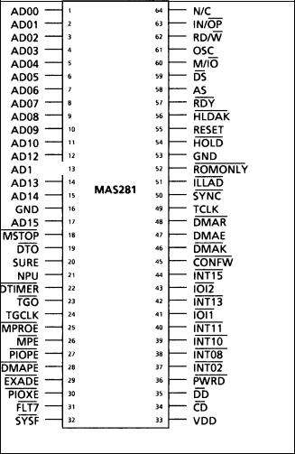
2.1PIN ASSIGNMENTS
Figure 4 defines the pin assignment for the MAS281 module. See section 10.0 for full packaging and pin assignment information.
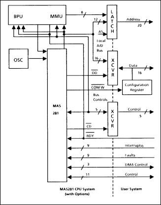
All signals - with the exception of power, ground and ROMONLYN - are TTL compatible. In addition, each function is provided with Electrostatic Discharge (ESD) protection circuitry. Figure 5 depicts a typical system implementation using many of these signals. Throughout this data sheet, active low signals are denoted either by placing a bar over the signal name, or by following the signal name with an “N” suffix, e.g., DDN. If a signal has a dual function, both function names will be used separated by a “/”. The function name to the left of the “/” will be active high while the function to the right will be active low, again with an “N" suffix, e g., RD/WN.
5/55
MAS281
2.2 PIN FUNCTIONS |
2.2.3 SYNCHRONIZATION CLOCK (SYNC) |
A description of each pin function follows. The function name is presented first, followed by its acronym and description. Function type is either input, output, high impedance (Hi-Z), or a combination thereof. Full timing characteristics of each of the functions are shown in section 6.0.
2.2.1 POWER AND GROUND (VDD & GND)
The MAS281 utilizes a single VDD power supply. A singlepoint ground is provided for the three chips on the substrate and is brought out on two module pins.
2.2.2 OSCILLATOR (OSC)
This input clocks the EU state sequencer which, in turn, generates timing and control signals for the rest of the module. To minimize skew between OSC edges and signals derived from OSC, and thereby optimize system performance, the OSC rise and fall times should be minimised. It is recommended that a clock driver with a high drive capability, such as a 54AS244, 54ALS244 or 54HST244, be used.
AD11
Figure 4: Pin Assignments
This active low output transitions from high to low to signal the start of a new machine cycle. It should be used as a timing reference for those operations which must be synchronized to the basic machine cycle.
SYNCN cycles associated with external memory or l/O bus transactions are a minimum of five OSC periods in duration and may be extended by inserting wait states via the external ready interface, For such cycles, a SYNCN low indicates that either an address or XlO command is on the AD bus; a high indicates data is on the bus. Wait states extend the high state of SYNCN.
SYNCN cycles associated with internal CPU operations, are either five or six OSC periods in duration. Six OSC periods are required for machine cycles associated with microcode branches or with the execution of internally decoded XlO commands. Five OSC periods are required for all other internal operations.
[Note: For modules operating at high OSC frequencies, the internal ready logic provided on the IU may cause a wait state to be inserted during execution of internal XlO commands. This would result in a SYNCN cycle of seven OSC periods duration. Though unlikely, this condition must be taken into account in implementing an external ready interface. Refer to the description of the Ready (RDYN) signal below for further details.]
SYNCN continues to cycle during DMA and HOLD states. Such cycles are five OSC periods in duration.
2.2.4 ADDRESS STROBE (AS)
Output/Hi-Z. This active high signal indicates that an address has been placed on the AD bus. This address is guaranteed valid at the high to low transition of AS. AS should be used to strobe an address latch during AD bus demultiplexing. This latch should be a transparent type for optimum performance. AS is placed in the high impedance state during DMA and Hold cycles and is held low during internal (non-XIO) operations.
2.2.5 DATA STROBE (DS)
Output/Hi-Z. This active low signal indicates that the AD bus is being used for data transfers. During read operations, DSN should be used by the selected external device to enable data onto the AD bus. This data is guaranteed valid on the low to high transition of DSN. The selected external device should use the low to high edge of DSN to perform the write. DSN is placed in the high impedance state during DMA and Hold cycles and is held high during internal (nonXlO) operations.
2.2.6 READ/WRITE (RD/W)
Output/Hi-Z, This dual function signal indicates the direction of data flow on the AD bus. A high level indicates a read operation with data being input to the module. A low level indicates a write operation with data being output by the module. RD/WN may be combined with DSN to generate separate read and write strobes. This signal goes valid shortly
6/55
after SYNCN goes low to indicate the start of a new machine cycle and remains valid until a new SYNCN cycle is begun, RD/WN is placed in the high impedance state during DMA and Hold cycles.
2.2.7 MEMORY/INPUT-OUTPUT (M/IO)
Output/Hi-Z, This dual function signal indicates the type of transfer of the AD bus that is occurring. A high state identifies memory transfers. A low state identifies l/O transfers. M/ION goes valid shortly after SYNCN goes low to indicate the start of a new machine cycle and remains valid until a new SYNCN cycle is begun. M/ION is placed in the high impedance state during DMA and Hold cycles and is held high during internal (non-XIO) operations.
Figure 5: Typical MAS281/MA31751 System Interface
MAS281
2.2.9 ADDRESS/DATA BUS (AD00 - AD15)
Input/Output/Hi-Z. AD00 through AD15 comprise a bidirectional multiplexed address and data bus which serves both as the communication path between the external system and module as well as the communication path among the three chips on the module. It is important to note that the AD bus is shared between the external system and internal module resources. To avoid bus contention during internal operations, the AD bus must be isolated from the external system through the use of a bus transceiver. A data direction signal (DDN) is provided for transceiver control .
Addresses, data and commands appearing on the AD bus are represented in positive logic. A high level indicates a logic 1 and a low level indicates a logic 0. AD00 is the most significant bit position whilst AD15 is the least significant bit position. The AD bus is placed in the high impedance state during the data portion of a read SYNCN cycle as well as during DMA and Hold cycles.
2.2.10 READY (RDY)
This asynchronous active low input is used by the EU state sequencer, in conjunction with the internal ready signal, to determine when the current machine cycle may be completed. By holding RDYN high, wait states may be inserted, stretching out the current machine cycle and allowing slower devices sufficient time to complete their operations.
[Note: If RDYN is held high during two consecutive TCLK high-to-low transitions (with DSN low), a bus timeout fault will occur and will be indicated in the appropriate bit in the fault register. The occurrence of this fault will cause the EU state sequencer to terminate the current machine cycle, drop SYNCN low, and begin a new machine cycle. Also, the presently executing macroinstruction will be aborted and execution will branch, unless masked, to the machine error interrupt (level 1) software routine. The DTON signal may be used to override this feature.]
2.2.11 CONTROL DIRECTION (CD)
This active low output goes high to indicate the module is driving the AS, DSN, M/ION, RD/WN and IN/OPN signals. During DMA and Hold cycles, this signal goes low to indicate the module has relinquished control of these signals and has placed them in the high impedance state. The DMA or Console controller, respectively, may then drive these signals. This signal should be used to control the transfer direction of the control signal transceiver.
2.2.8 INSTRUCTION/OPERAND (IN/OP) |
2.2.12 DATA DIRECTION (DD) |
Output/Hi-Z. This dual function signal indicates the type of data on the AD bus during the data portion of a SYNCN cycle. A high state identifies an instruction while a low state identifies an operand. IN/OPN goes valid shortly after SYNCN goes low to indicate the start of a new SYNCN cycle and remains valid until a new SYNCN cycle is begun. This signal is required during expanded memory accesses. IN/OPN is placed in the high impedance state during DMA and Hold cycles.
This active low signal indicates the direction of data transfer on the AD bus. This signal goes high to indicate a write transfer from the module to the external system. It also goes high during all internal module operations. DDN goes low to indicate a read transfer from the external system to the module. It also goes low during DMA and Hold cycles as well as during configuration register reads.
[Note: In addition to going high during the execution of internally implemented XIO commands, DDN also goes high
7/55
MAS281
during execution of XIO commands which are implemented in the MA31751 MMU(BPU) chip.
If an MA31751 is used with the MAS281, it must reside on the MAS281 local AD bus rather than the system buses (see Figure 5). Table 7b in Section 4.0 identifies those XIO commands which are implemented in the MA31751].
2.2.13 DIRECT MEMORY ACCESS ENABLE (DMAE)
This active high output goes high in response to the DMAE XIO command. A high state indicates DMA requests will be acknowledged; a low state indicates a DMA request will be ignored.
2.2.14 DIRECT MEMORY ACCESS REQUEST (DMAR)
A low on this asynchronous active low input will cause the processor to suspend internal operations at the end of the current machine cycle. This request will only be acknowledged by the module when DMAE is high.
2.2.15 DIRECT MEMORY ACCESS ACKNOWLEDGE (DMAK)
This active low signal goes low in response to a DMA request if DMAE is high. A low state grants use of the system busses to the requesting DMA device by placing the module’s AD bus, AS, DSN,RD/WN, M/ION and IN/OPN drivers into the high impedance state and by pulling CDN and DDN low. The high-to-low transition is synchronized to the falling edge of SYNCN to ensure that the current machine cycle is completed before the DMA device is granted the bus. DMAKN will remain low until the requesting device raises DMARN.
2.2.16 HOLD REQUEST (HOLD)
A low on this asynchronous active low input will cause the module to suspend internal processor functions at the end of the currently executing MIL-STD-1750A instruction. A Hold state is also entered if the processor encounters a breakpoint (BPT) instruction and the configuration word indicates the presence of a Console (bit 15 = 0).
[Note: Hold should be syncronised to the AS signal.]
2.2.17 HOLD ACKNOWLEDGE (HLDAK)
This active low output goes low either upon completion of the MIL-STD-1750A instruction during which HOLDN went low or if the processor encounters a breakpoint (BPT) instruction with Console present indicated in the configuration word register. A low on this signal indicates to the requesting device that that the module AD bus, AS, DSN, M/ION, RD/WN, and IN/OPN drivers have been placed in the high impedance state. The Hold state is terminated either by raising HOLDN high or, in the case of a BPT caused Hold, by pulsing HOLDN low and high again (see Section 6.0).
2.2.18 SYSTEM RESET (RESET)
This asynchronous active high input should be raised high to reset the module. The high-to-low transition of this input will start the module’s initialization.
2.2.19 START-UP ROM ENABLE (SURE)
This active high output goes high during initialization and may also be asserted by software with the ESUR XIO command. This signal remains high until removed by software via the DSUR XIO command. When a Start-Up ROM is present, this signal should be used to qualify its chip select or output enable input such that the ROM may be accessed only when SURE is high.
[NOTE: Instruction pipelining must be considered in transitioning from Start-Up ROM to RAM when using the DSUR XIO command. If a system overlays RAM with the StartUp ROM and transitions to execution from RAM by simply executing DSUR from the ROM, then IA will contain the value stored in the ROM location immediately following DSUR. This value will be treated as an instruction and the module will attempt to execute it. In such cases, it is recommended that DSUR be followed by an unconditional branch instruction with offset, i e, the BR instruction. An alternative approach is simply to jump to a portion of RAM not overlaid by the Start-Up ROM and execute DSUR from RAM.]
2.2.20 CONFIGURATION WORD (CONFW)
This active low output goes low when the module reads the external configuration register and should be used as that register’s output enable strobe (see Section 6.0). Table 1 defines the required format of the configuration register. A zero in a given bit position indicates the specified device is present. Bits 0 through 11 are not used by the module.
The configuration register is read during initialization to determine the system configuration. It is also read whenever a (BPT) instruction is executed to determine the presence of a Console. If a console is not present, a BPT will be interpreted as a NOP. DDN goes low during a configuration register read. Thus, the configuration register must reside on the system AD bus rather than the local AD bus (see Figure 5).
2.2.21 NORMAL POWER UP (NPU)
This active high output is dropped low during module initialization as the first step of BIT. If BIT is successful, NPU goes high and remains high until reset by software via the RNS XIO command. NPU cannot be set high by software.
2.2.22 TIMER CLOCK (TCLK)
This clock input is used by interval timers A and B as well as the interface fault timer. Timer A is clocked at the TCLK frequency while timer B is clocked at a frequency of TCLK/10. MIL-STD-1750A requires that this input be a 100kHz pulse train.
8/55
Bit |
Device |
|
|
15 |
Console |
|
|
14 |
MMU |
|
|
13 |
BPU |
|
|
12 |
Output Discrete Register |
|
|
11-0 |
Unused |
|
|
Table 1: Configuration Register Bit Assignment
2.2.23 TRIGGER-GO CLOCK (TGCLK)
This clock input is used by the internal 16-bit trigger-go counter. The trigger-go counter counts at the same frequency as TGCLK.
2.2.24 TRIGGER-GO DISCRETE (TGO)
This active low output goes low whenever the trigger-go counter overflows, i e., the counter rolls over to 0000. It returns to the high state when the trigger-go counter is reset by software via the GO XIO command.
2.2.25 DISABLE TIMER (DTIMER)
A low on this active low input disables timers A and B as well as the trigger-go counter. A low also disables DMA access by forcing DMAE low and DMAKN high. Raising DTIMERN allows timers A and B and the trigger-go counter to resume counting from the value at which they were stopped. A high also allows normal DMA operation.
2.2.26 DISABLE TIMEOUT (DTO)
A low on this active low input will reset and disable the bus fault timeout circuitry.
2.2.27 POWER DOWN INTERRUPT (PWRD)
A low on this active low input is captured in the Pl register by a SYNCN high-to-low transition. This sets pending interrupt 0. This is the highest priority interrupt and cannot be masked or disabled.
2.2.28 USER INTERRUPTS (INT02,08,10,11,13 AND 15)
A low on any of these active low inputs will be captured in the Pl register by a SYNCN high-to-low transition and will set pending interrupt levels 2, 8, 10, 11, 13, and 15, respectively. Level 2 is the highest priority user level while level 15 is the lowest priority. These interrupts are maskable and can be disabled. Unused inputs should be pulled up to VDD.
[NOTE: The INTO2 service routine should clear the PI Register using the RPI 0002 instruction.]
MAS281
2.2.29 I/0 DEDICATED INTERRUPTS (IOI1 & IOI2)
A low on either IOI1N or IOI2N will be captured in the Pl register by a SYNCN high-to-low transition and will set pending interrupt levels 12 and 14, respectively. Unused inputs should be pulled up to VDD.
[NOTE: Interrupt levels 1, 3, 4, 5, 6, 7, and 9 are dedicated to internal machine interrupts.]
2.2.30 MEMORY PROTECT ERROR (MPROE)
A low on this active low input, captured by the SYNCN high-to-low transition, is used to inform the module that an access fault, execute protect, or write protect violation has been detected. Bit O of the module Fault Register (FT) is set if this signal goes low during a memory cycle; bit 1 is set if it goes low during a DMA cycle. Either condition immediately sets pending interrupt level 1 and in the case of a memory cycle error, causes the currently executing MIL-STD-1750A instruction to be aborted.
Although the MAS281 aborts the macroinstruction, system memory management, and / or block protect hardware is responsible for preventing the erroneous bus cycle from accessing memory. To effectively use this feature, MPROEN should be pulled low prior to the high-to-low SYNCN transition of the next machine cycle. This can easily be accomplished by injecting wait states to hold off the DSN rising edge (write cycle) and the SYNCN falling edge (read cycle) until the system protection circuitry can decide whether or not to allow the transaction.
2.2.31 MEMORY PARITY ERROR (MPE)
A low on this active low input, captured by the SYNCN high-to-low transition, is used to inform the module that a parity error has been detected during a memory transfer. Bit 2 of the module Fault Register (FT) is set when this signal goes low. This, in turn, causes pending interrupt level 1 to be set.
2.2.32 PROGRAMMED I/O PARITY ERROR (PIOPE)
A low on this active low input, captured by the SYNCN high-to-low transition, is used to inform the module that a parity error has been detected during an external l/O transfer. Bit 3 of the module Fault Register (FT) is set when this signal goes low. This, in turn, causes pending interrupt level 1 to be set.
2.2.33 DMA PARITY ERROR (DMAPE)
A low on this active low input, captured by the SYNCN high-to-low transition, is used to inform the module that a parity error has been detected during a DMA data transfer. Bit 4 of the module Fault Register (FT) is set when this signal goes low This, in turn, causes pending interrupt level 1 to be set.
2.2.34 EXTERNAL ADDRESS ERROR (EXADE)
A low on this active low input, captured by the SYNCN high-to-low transition, is used to inform the module that a system address error has been detected. Bit 8 of the module Fault Register (FT) is set when this signal goes low during a
9/55

MAS281
memory fault; bit 5 is set if it goes low during an l/O fault. As with MPROEN, either condition immediately sets pending interrupt level 1 and causes the currently executing MIL-STD- 1750A instruction to be aborted .
2.2.35 PROGRAMMED I/O TRANSFER ERROR (PIOXE)
A low on this active low input, captured by the SYNCN high-to-low transition, is used to inform the module that a programmed l/O data transfer error has been detected. Bit 6 of the module Fault Register (FT) is set when this signal goes low. This, in turn, causes pending interrupt level 1 to be set.
2.2.36 FAULT #7 (FLT7)
A low on this active low input, captured by the SYNCN high-to-low transition, sets bit 7 of the Fault Register (FT). This is a user definable fault.
2.2.37 SYSTEM FAULT (SYSF)
A low on this active low input, captured by the SYNCN high-to-low transition, sets bits 13 and 15 of the Fault Register (FT). This is a user definable fault.
2.2.38 ILLEGAL ADDRESS (ILLAD)
This active low output drops low if the EXADEN input drops low or if the bus fault timeout circuit causes an interface timeout.
2.2.39 MICROCODE STOP (MSTOP)
MSTOPN allows microcode to be single-stepped and is reserved for use by GEC Plessey Semiconductors. MSTOPN must be pulled up to VDD in customer applications.
2.2.40 ROM ONLY (ROMONLY)
ROMONLYN is used for testing by GEC Plessey Semiconductors and must be pulled up to VDD in customer applications.
3.0 OPERATING MODES
MAS281 operating modes include: (1) initialisation, (2) instruction execution, (3) interrupt servicing, (4) fault servicing,
(5) DMA support, (6) Hold support, and (7) timer operations.
3.1 INITIALISATION
The module executes a microcoded initialisation routine in response to a hardware reset. This routine clears module registers, disables and masks interrupts, reads the configuration register, resets the output discrete register (if implemented), initialises the MMU and BPU (if implemented), performs Built-ln-Test (BIT), raises the Start-Up ROM enable discrete, clears and starts timers A and B, resets the trigger-go
counter, and loads the instruction pipeline. Table 2 summarises the resulting initialisation state, and Table 3 provides a detailed breakdown of the initialisation sequence.
BIT consists of five subroutines, as outlined in table 4, and begins by pulling NPU low. This is the first time after reset that NPU is guaranteed low. If all five subroutines execute successfully, NPU is raised high. If any part of BIT fails, an error code identifying the failed subroutine is loaded into the Fault Register (FT), BIT is aborted, and NPU is left in the low state. Table 4 defines the coding of BIT results in FT. In the event of such a failure, the resulting module reset state will be dependent on where in BIT the error occurred and may not be the same as that shown in Table 2. A BIT failure indication in FT will set the level 1 interrupt request bit of the Pending Interrupt (Pl) register. Since initialisation disables and masks interrupts, this interrupt request will not be asserted .
The last action performed by the initialisation routine is to load the instruction pipeline. Instruction fetches start at memory location zero and will be from the Start-Up ROM if implemented. Whether BIT passes or not, the processor will begin instruction execution at this point.The system start-up code may include a routine to enable and unmask interrupts in order to detect and respond to a BIT failure.
[NOTE: To complete initialisation and pass BIT, interrupt and fault inputs must be high for the duration of the initialisation routine. Also, timers A and B must be clocked during this interval, i.e., TCLK must be applied.]
MAS281
Instruction Counter (IC) |
Zeroed |
Status Word (EU and MMU) (SW) |
Zeroed |
Fault (FT) |
Zeroed |
Pending Interrupt (PI) |
Zeroed |
Mask (MK) |
Zeroed |
Interrupts |
Disabled |
DMA Access |
Disabled |
Timer A |
Reset and Started |
Timer B |
Reset and Started |
Trigger-Go Timer |
Reset and Started |
|
|
MMU |
|
Page Registers |
Group 0 Enabled |
AL, W, E Fields |
Zeroed |
PPA Field |
Logical to Physical |
|
Map |
|
|
BPU |
|
Write Protect |
Zeroed |
Global Memory Protect |
Enabled |
Table 2: Initialisation State
10/55
MAS281
Label |
Cycle |
|
|
|
|
|
|
MAIN |
B 1 |
1. Enable Control of DMAE Output signal |
|
|
P |
2. - |
|
|
B1 |
3. Clear MAS281 Execution Unit Status Word (SW) |
|
|
|
Clear Interrupt Mask (MK) (Internal l/O command, SKM 2000H) |
|
|
B1 |
4. Clear Pending Interrupt Register (Pl) and Fault Register (FT) (Internal l/O Command, CLIR,2001 H) |
|
|
|
Clear Instruction Counter (IC) |
|
|
P |
5. - |
|
|
B1 |
6. Disable Interrupts (Internal l/O Command, DSBL,2003H) |
|
|
P |
7. - |
|
|
B1 |
8. Clear MMU Status Word (Internal l/O Command, WSW, 200EH) (Note 1) |
|
|
P |
9. - |
|
|
B1 |
10. |
Disable DMA Access (lnternal l/O Command, DMAD, 4007H) |
|
P |
11. |
- |
|
B1 |
12. |
Read Configuration Register (Internal l/O Command, RCW, 8400H, CONFWN Drops low per Figure 25, |
|
|
|
Section 5.0) |
|
P |
13. |
- |
|
P |
14. |
- |
|
B2 |
15. |
- (If Output Discrete Register Present, then Continue; Else, Skip to 18.) |
|
P |
(16). - |
|
|
I/O |
(17). Clear Output Discrete Register (External l/O Command) |
|
|
P |
18. |
- |
|
B2 |
19. |
- (If BPU present, then Branch to BPU; else, continue) |
|
P |
20. |
- |
|
B2 |
21. |
- (If MMU present, then Branch to MMU, Else, Continue) |
|
P |
22. |
- (Setup Temporary Register to indicate No MMU Present) |
|
B2 |
23. |
- (Branch to MAS281 BIT) |
|
P |
24. |
- |
|
B1 |
25 Enable Start-Up ROM (Internal l/O Command, ESUR,4004H; SURE Raises High per Figure 25, |
|
|
|
|
Section 5.0) |
|
P |
26. |
- |
|
B1 |
27. |
Clear and Start Timer A (Internal l/O Command, OTA,400AH) |
|
B1 |
28. |
Reset the Trigger-Go timer (mternal l/O Command, GO,400BH) |
|
P |
29. |
- |
|
B1 |
30. |
Clear and Start Timer B (Internal l/O Command, OTB,400EH) |
|
B2 |
31. |
- (Branch to Load Instruction Pipeline Routine) |
|
M |
32. |
Load data-ln register (Dl) and instruction Register A (IA) from [IC] Increment IC |
|
M |
33. |
Load Data-ln Register (Dl) and Instruction Register a (IA) from [IC] ([lA] Moves to IB), Increment IC, |
|
|
|
Map Instruction Register B (IB) into Mlcrocode Routine |
BPU |
P |
(1). - |
|
|
P |
(2). - (Set Loop to Clear Memory Protect RAM) |
|
|
I/O |
(3). Clear a Location in MPRAM (Internal l/O Command, LMP,50XXH), Increment Address, Do 128 Times |
|
|
|
(4). - (Branch Back to 20 ) |
|
MMU |
P |
(1). - |
|
|
P |
(2). - |
|
|
P |
(3). - (Setup Loop to Load Instructlon Page Registers (IPR) and Operand Page Registers (OPR) with |
|
|
|
|
Sequential Values of 0 to 255) |
|
P |
(4). - |
|
|
P |
(5). - |
|
|
I/O |
(6). Load a Location in the IPR wlth the value of the Location Address (Internal l/O Command, WIPR, |
|
|
|
|
51 XYH) |
|
I/O |
(7). Load a Location in the OPR Increment Loaded Value with the Value of the Location Address (Internal |
|
|
|
|
I/O Command. WOPR,52XYH) |
|
P |
(8). - (Increment IPR Address) |
|
|
P |
(9). - (Increment OPR AddressRepeat Loop 14 - 9 1256 Times) |
|
|
B2 |
(10). - (Setup Temporary Register to Indlcate MMU Present; Branch back to 23) |
|
|
|
|
|
Notes:
1.This operation is performed whether or not an MMU is present.
2.“-” indicates internal CPU operation
3.Sequence numbers in “( )” are performed only under the stated conditions.
4.Each step enumerated above represents a single machine (SYNC) cycle of the type shown in the “Cycle” column.
“P” indicates a 5 OSC cycle,60% duty cycle, machine cycle.
“I/O” and “M” Indicate a 5 OSC cycle,50% duty cycle, machine cycle. “B1” indicates a 6 OSC cycle 50% duty cycle machine cycle.
“B2” indicates a 6 OSC cycle 66% duty cycle machine cycle
Table 3: MAS281 Initialisation Sequence
11/55
MAS281
3.2 INSTRUCTION EXECUTION
Once initialisation has been completed, the module will begin instruction execution. Instruction execution is characterised by a variety of operations, each one or more machine cycles in duration. Depending on the instruction being executed at the time, these operations include: (1) internal CPU cycles, (2) instruction fetches, (3) operand transfers, and (4) input/output transfers. Instruction execution may be interrupted at the end of any individual machine cycle by DMA operations and at the conclusion of any given instruction by an interrupt or Hold request.
3.2.1 INTERNAL CPU CYCLES
Internal CPU cycles are used to perform all CPU data manipulation and housekeeping operations. Internal CPU cycles are either five or six oscillator periods in duration and are characterised by AS low and DSN, DDN and M/ION high. Section 6.0 provides timing characteristics for internal CPU cycles. Tables 7a and 7b in Section 4.0 provide machine cycle counts (both the five and the six OSC cycle variety) associated with each MIL-STD-1750A instruction.
3.2.2 INSTRUCTION FETCHES
Instruction Fetches are used to keep the instruction pipeline full. This ensures that the next instruction is always ready for execution when the preceding instruction is completed. During jump and branch instruction execution, the pipeline is flushed, and then it is refilled via two consecutive instruction fetches starting at the new instruction location. The pipeline is also refilled as part of interrupt and hold request processing.
Instruction fetches are characterised by IN/OPN high but are otherwise identical to an operand read transfer. For a detailed explanation of the function of various bus control signals during instruction fetches, refer to the discussion of operand transfers below. Section 6.0 provides timing characteristics for instruction fetches. Machine cycles associated with instruction fetches are a minimum of five oscillator periods in duration. The RDYN signal may be used to insert wait states to accommodate slow memory. Machine cycle counts included in Table 7a of Section 4.0 include instruction fetches.
Instruction fetches use instruction pipeline registers IA and IB, the instruction counter (IC), and the data input register (Dl) and proceed as follows: assuming an empty instruction pipeline (occurring as a result of a reset, jump, or branch), the contents of IC are placed on the AD bus as an address. The returned value, which will be an instruction, is stored in the IA register.
The value in IC is incremented (via its dedicated counter) and the next fetch is performed. This second returned value, which may be either an instruction or an immediate operand, is stored in both the IA and Dl registers. The instruction previously stored in IA is advanced to IB to be executed.
The instruction in IB is checked to determine if an immediate operand is required. If so, that operand has already been pre-fetched and resides in both IA and Dl. If not, then the value currently in IA is an instruction. If IA contains an operand,
another instruction fetch is performed and the returned value is stored only in IA (the contents of IB and Dl are preserved). If IA contains an instruction, however, the next fetch is deferred until the contents of IB are no longer needed. At that time, the deferred fetch is performed, IA is advanced to IB for execution, and the newly returned value is stored in both IA and Dl.
This sequence repeats until the instruction pipeline is again emptied at which time the whole process is repeated .
3.2.3 OPERAND TRANSFERS
Operand transfers are used to obtain (read in) operands to be used by an instruction and to save (write out) any results of an instruction’s execution. Section 6.0 provides timing characteristics for operand transfers. Machine cycles associated with operand transfers are a minimum of five oscillator periods in duration. The RDYN signal may be used to insert wait states to accommodate slow memory. Machine cycle counts in Table 7a of Section 4.0 include operand transfers.
Operand transfers use the address register (A), the data input register (Dl), and data output register (DO). Before the operand transfer begins, the processor calculates the effective operand address and stores this value in A. For write transfers, the processor loads the operand into the DO register.
All operand transfers between the module and memory are referenced to the AS and DSN bus control signals and are characterised by IN/OPN low and, by M/ION and CDN high. The transfer begins by placing the contents of A (the address register) on the AD bus immediately following the SYNCN high-to-low transition. The AS strobe then goes high to enable the system’s transparent address latch. The address is assured valid on the high-to-low transition of AS. The DDN signal is high during the address portion of the transfer; its subsequent action depends on whether the transfer is a read or write.The RDWN signal indicates the direction of the transfer. If the operand is a write, the address from A is replaced by the operand in DO when SYNCN transitions from low-to-high. Next, the DSN signal goes low and can be used by the memory system to generate a write enable. Data is guaranteed valid at the low-to-high transition of DSN. DDN stays high for the duration of a write transfer. The memory system must pull RDYN low to conclude the transfer.
If the operand transfer is a read, the AD bus drivers are placed in a high impedance state at the low-to-high transition of SYNCN to give the memory system access to the bus. Next, the DSN signal goes low and can be used by the memory system to generate an output enable. Shortly after DSN goes low, DDN also goes low. This should be used by the system to reverse the direction of the system’s AD bus transceivers. The memory system must pull RDYN low to conclude the transfer. Data will be read into the Dl register on the SYNCN high-to-low transition 3.2.4 Input/Output Transfers
Input/Output transfers utilize the MIL-STD-1750A XIO and VIO protocols and are characterized by M/ION and IN/OPN low and CDN high. RD/WN defines the direction of the transfer. AS and DSN cycle as with operand transfer operations. The procedure followed depends on whether the transfer is associated with one of the internally implemented XIO commands or an externally implemented capability. An exception is the Read Configuration Word (RCW) command
12/55
which is decoded by the MAS281 but is treated, in some ways, like an externally implemented XIO command. This exception is discussed below.
Internal l/O transfers involve all XIO commands which are decoded internally either by the MAS281 or by the MA31751 MMU/BPU chip (with the exception noted above). Table 7b identifies these commands. The A, Dl and DO registers are used as in operand transfers. Internal l/O transfers are characterised by DDN staying high for the duration of the transfer in order to prevent bus contention between the module AD bus and the system bus. Machine cycle associated with internal I/O commands are normally six oscillator cycles in duration but might be extended to seven OSC cycles by the internal ready interface if the module is run at high frequencies. Internal I/O transfers may be subdivided into writes, reads and commands as follows:
I/O writes consist of a command phase followed by the value to be written. The command is placed on the AD bus from the A register at the SYNCN high-to-low transition and is assured valid on the high-to-low transition of AS. The value to be written is placed on the AD bus from the DO register at the SYNCN low-to-high transition and is written to the internal l/O device by the subsequent SYNCN high-to-low transition. An example of an internal l/O write is loading timer A.
I/O reads consist of a command phase followed by the value returned by the internal device. The command is placed on the AD bus from the A register at the SYNCN high-to-low transition and is assured valid on the highto-low transition of AS. The internal l/O device places the value to be read on the
MAS281
AD bus at the SYNCN low-tohigh transition. This value is captured by the Dl register on the subsequent SYNCN high-to- low transition. An example of such an operation is reading the interrupt mask register.
I/O commands consist of a command phase alone. The command is placed on the AD bus from the A register at the SYNCN high-to-low transition and is executed at the following SYNCN high-to-low transition. An example of an l/O command is raising the DMAE discrete.
External l/O transfers are similar to internal l/O transfers with the following exceptions: (1) DDN goes low, as with operand transfers, during an l/O read; and (2) external l/O machine cycles are normally five OSC cycles in duration and may be extended via the RDYN signal as with operand transfers.
As discussed earlier, the Read Configuration Word command is a special case. It is decoded internally to generate a read strobe (CONFWN) and therefore uses both the standard internal I/O six OSC period machine cycle as well as the internal ready interface to extend its cycle. It relies on an externally implemented configuration register, however, and therefore cycles DDN as with external I/O cycles. Therefore, the configuration word register must reside on the system side of the data bus transceivers as opposed to residing directly on the local AD bus (as shown in Figure 5).
Nine user interrupt request inputs are provided for programmed response to asynchronous system events. A low on any of these inputs will be detected at the high-to-low transition of SYNCN and latched into the Pending Interrupt (Pl)
BIT |
Test Coverage |
BIT Fail Codes (FT 13,14,15) |
Cycles |
|
|
|
|
1 |
Microcode Sequencer |
|
|
|
IB Register Control |
100 |
220 |
|
Barrel Shifter |
|
|
|
Byte Operations and Flags |
|
|
|
|
|
|
2 |
Temporary Registers (T0 - T7) |
|
|
|
Microcode Flags |
101 |
165 |
|
Multiply |
|
|
|
Divide |
|
|
|
|
|
|
3 |
Interrupt UnitMK, Pl, FT |
111 |
216 |
|
Enable/Disable Interrupts |
|
|
|
|
|
|
4 |
Status Word Control |
|
|
|
User Flags |
110 |
155 |
|
General Registers (R0 - R15) |
|
|
|
|
|
|
5 |
Timer A |
111 |
775 |
|
Timer B |
|
|
|
|
|
|
- |
BIT Pass/Fail Overhead |
- |
25 |
|
|
|
|
Note: BIT pass is indicated by all zeros in FT bits 13,14, and 15.
Table 4: Built-in Test Coverage and Tuning
13/55

MAS281
register on the following SYNC high-to-low transition (with the |
|
|
|
|
|
|
|
|
exception of INT02N which is latched into Pl when INT02N is |
|
|
|
|
|
|
|
|
first detected). This sequence occurs whether interrupts are |
|
|
|
|
|
|
|
|
enabled or disabled or whether the specific interrupt is masked |
|
|
|
|
|
|
|
|
or unmasked. |
|
|
|
|
|
|
|
|
Each external Pl register input is buffered by a falling edge |
|
|
|
|
|
|
|
|
detector to prevent repeat latching of requests held low |
|
|
|
|
|
|
|
|
beyond the first SYNCN high-to-low transition. An interrupt |
|
|
|
|
|
|
|
|
request input must transition to the high state before a |
|
|
|
|
|
|
|
|
subsequent request on that input will be detected. |
|
|
|
|
|
|
|
|
When an interrupt request is latched into Pl, it is ANDed |
|
|
|
|
|
|
|
|
with its corresponding mask bit in the mask register (MK). |
|
|
|
|
|
|
|
|
Interrupt level 0 is not maskable. Any unmasked pending |
|
|
|
|
|
|
|
|
|
|
|
|
|
|
|
|
|
interrupts are output to the priority encoder where the highest |
|
|
|
|
|
|
|
|
priority is encoded as a 4-bit vector. If interrupts are enabled, |
|
|
|
|
|
|
|
|
and an unmasked interrupt is pending, the priority encoder will |
|
|
|
|
|
|
|
|
assert an interrupt request to the CU. |
|
|
|
|
|
|
|
|
|
|
|
|
|
|
|
|
|
Upon completing execution of a given MIL-STD-1750A |
|
|
|
|
|
|
|
|
instruction, the CU’s microsequencer checks the state of the |
|
|
|
|
|
|
|
|
priority encoder’s interrupt request. If an interrupt request is |
|
|
|
|
|
|
|
|
asserted, the microsequencer branches to the microcode |
|
|
|
|
|
|
|
|
interrupt service routine. This routine performs a read of the |
|
|
|
|
|
|
|
|
priority encoder’s 4-bit pending interrupt vector, stores the |
|
|
|
|
|
|
|
|
value in the EU Dl register, and then uses this value to |
|
|
|
|
|
|
|
|
calculate the appropriate interrupt linkage and service |
|
|
|
|
|
|
|
|
|
|
|
|
|
|
|
|
|
pointers. The pointers serve as addresses to data structures |
|
|
|
|
|
|
|
|
|
|
|
|
|
|
|
|
|
used in servicing interrupts. Figure 6 depicts this relationship. |
|
|
Figure 6: Interrupt Vectoring |
|
|
|||
Table 5 defines pointer values. |
|
|
|
|
||||
|
|
|
|
|
|
|
|
|
Using the linkage and service pointers, the microcode |
|
|
|
|
|
|
|
|
interrupt service routine performs the following: (1) the current |
|
|
|
|
|
|
|
|
contents of the status word, mask register, and instruction |
|
|
|
|
LP |
SP |
|
|
counter are saved; (2) a write status word l/O command is |
|
|
Interrupt |
Address |
Address |
|
|
|
executed with an all zero data word; (3) the new mask is |
|
|
|
|
|
|
|
|
loaded into MK and interrupts are disabled; (4) the new status |
PWRD |
|
0 |
|
20 |
21 |
|
|
word is read and checked for a valid AS field - If AS is non-zero |
|
|
1 |
|
22 |
23 |
|
|
and an MMU is not present, AS is set to zero and fault 11 |
INT02 |
|
2 |
|
24 |
25 |
|
|
(address state error) is set in the fault register FT; (5) a write |
|
|
3 |
|
26 |
27 |
|
|
status word command using the new status word is performed; |
|
|
4 |
|
28 |
29 |
|
|
and (6) the new IC value is loaded into IC, the instruction |
|
|
5 |
|
2A |
2B |
|
|
pipeline is filled starting at the new address, and instruction |
|
|
6 |
|
2C |
2D |
|
|
execution begins. |
|
|
|
|
|
|||
|
|
7 |
|
2E |
2 F |
|
|
|
[NOTE: The steps listed above represent a summary of |
|
|
|
|
|
|||
INT08 |
|
8 |
|
30 |
31 |
|
|
|
actions performed during interrupt servicing and do not |
|
|
|
|
||||
|
|
9 |
|
32 |
33 |
|
|
|
necessarily reflect the actual order in which these events take |
|
|
|
|
|
|||
INT10 |
|
10 |
|
34 |
35 |
|
|
|
place.] |
|
|
|
|
||||
INT11 |
|
11 |
|
36 |
37 |
|
|
|
If an interrupt is latched during the interrupt service routine, |
|
|
|
|
||||
IOI1 |
|
12 |
|
38 |
39 |
|
|
|
it will not be processed until interrupts are re-enabled. If an AS |
|
|
|
|
||||
INT13 |
|
13 |
|
3A |
3B |
|
|
|
fault occurs during the service routine, interrupt level 1 will be |
|
|
|
|
||||
IOI2 |
|
14 |
|
3C |
3D |
|
|
|
set. This interrupt will be serviced when interrupts are re- |
|
|
|
|
||||
INT15 |
|
15 |
|
3E |
3F |
|
|
|
enabled unless it is masked by the new value in MK. |
|
|
|
|
||||
|
|
|
|
|
|
|
|
|
3.4 FAULT SERVICING |
|
Table 5: Interrupt Pointer Definitions |
|
|
||||
|
|
|
|
|
|
|
|
|
Eight user fault inputs are provided. A low on any of these |
|
|
|
|
|
|
|
|
inputs will be latched into the Fault Register (FT) at the high-to- |
|
|
|
|
|
|
|
|
low transition of SYNCN. |
|
|
|
|
|
|
|
|
14/55
No falling edge detectors are provided to prevent repeat latching of faults held low beyond the first SYNCN high-to-low transition. However, all FT bits are ORed together and input to the Pl bit 1 through an edge detector to prevent the fault register from causing multiple level 1 interrupts.
The sequence of events following a fault capture depends on the type of fault as follows:
3.4.1 MPEN, PIOPEN, DMAPEN, PIOXEN, FLT7N, AND SYSFN
The capture of one or more of these faults immediately sets pending interrupt level 1 (machine error) of the Pending Interrupt (Pl) register. Anti-repeat logic between the FT and Pl prevents latching more than a single interrupt into the Pl before the user interrupt service routine has cleared the FT. The microcoded interrupt service routine reads the interrupt priority vector from the Interrupt Unit and clears the service interrupt from the Pl. At this point the Pl is ready to latch another interrupt into this bit.
When this microcoded service routine acts on a level 1 interrupt, it clears the Pl bit 1, but the FT maintains the interrupting bit(s). Therefore, a level 1 interrupt would be latched again if there was no anti-repeat logic to prevent a never-ending loop of interrupts.
During the SYNCN cycles between fault capture and the beginning of the microcode interrupt handling routine, AS and DSN are forced to their inactive states. In the case of MPROEN, which may reflect an attempted write violation, it is required that system hardware provide the additional protection necessary to inhibit memory write strobe.
Interrupts are serviced at the end of the currently executing instruction if not masked and if interrupts are enabled. System software servicing level 1 interrupts must clear the FT via the RCFR internal l/O command at some point in the routine to allow subsequent faults to latch a level 1 interrupt request. A non-destructive read of the FT is provided by the internal l/O command RFR, but this command should be used carefully.
3.4.2 MPROEN, EXADEN, AND BUS FAULT TIME-OUT
The capture of one or more of these faults immediately sets pending interrupt level 1 (machine error) of the Pending Interrupt (Pl) register. Furthermore, the instruction currently executing is aborted at the SYNCN high-to-low transition following the SYNCN high-to-low transition that latched the fault. The IC value saved in the interrupt linkage table for the level 1 interrupt always points to the instruction which was in instruction pipeline register IA at the time of the abort. Antirepeat logic between the FT and Pl prevents latching more than a single interrupt into the Pl before the user interrupt service routine has cleared the FT.
The microcoded interrupt service routine reads the interrupt priority vector from the Interrupt Unit and clears the serviced interrupt from the Pl. At this point the Pl is ready to latch another interrupt into this bit. When this microcoded service routine acts on a level 1 interrupt, it clears the Pl bit 1, but the FT maintains the interrupting fault bit(s). Therefore, a level 1 interrupt would be latched again if there were no antirepeat logic to prevent a never-ending loop of interrupts from occurring .
MAS281
3.5 DMASUPPORT
DMA data transfers are performed under the control of a system DMA controller over the system AD bus. The user signals that DMA requests will be honored by setting the DMAE output high via the DMAE internal XlO command. The DMA controller may request use of the AD bus by pulling the module’s DMARN input low.
Unless the DMAE output is high, all such requests will be ignored. If DMAE is high, DMARN will be acknowledged by DMAKN dropping low. This occurs at the first SYNCN high-to- low transition after DMARN goes low.
DMAKN low indicates that the module has relinquished control of the AD bus by placing its AD bus, AS, DSN, M/ION, RD/WN and IN/OPN drivers in their high impedance state. DDN is dropped low to direct the system data bus transceivers to drive the local AD bus and CDN is dropped low to disable the control signal buffers. The DMA controller relinquishes control of the AD bus by raising DMARN high. The module responds by raising DMAKN high at the next SYNCN high-to- low transition and continuing with program execution.
3.6 HOLD SUPPORT
The Hold state is provided to facilitate debugging of user software by allowing the user to disable the MAS281 and access system resources. Hold state timings is defined in Section 6.0. The Hold state can be entered either by pulling HOLDN low or by executing a BPT instruction with the Console present and indicated in the Configuration Word. These two approaches, as well as methods for using the Hold state to single step through software, are discussed below:
3.6.1 USING HOLDN
At the completion of the currently executing instruction, the microsequencer checks the state of the HOLDN input. If low, the microsequencer branches to the microcode Hold service routine. This routine decrements IC twice, enables the Hold termination sequence, drops HLDAKN low, and enters the Hold state. HLDAKN drops low three SYNCN cycles after the final SYNCN cycle of the currently executing instruction. A low on HLDAKN indicates that the module has relinquished the AD bus by placing its AD bus, AS, DSN, M/ION, RD/WN and IN/ OPN drivers into the high impedance state and, DDN and CDN drop low.
When HOLDN is returned high, the Hold state will end on the subsequent high-to-low transition of SYNCN. This is signified by raising HLDAKN, at which point thc module resumes control of the AD bus, AS, DSN, M/ION, RD/WN and IN/OPN signals. CDN and DDN raise high.Thc instruction pipeline is then refilled and instruction execution resumes with the first instruction loaded into the pipeline
15/55

MAS281
Figure 7: Pending Interrupt Register Bit Assignments |
Figure 8: Fault Register Bit Assignments |
3.6.2 USING BPT
The Hold state may also be entered by executing a BPT instruction with Console present indicated in the Configuration Word. On encountering a BPT instruction, the processor reads the Configuration Word to check for the presence of a Console. If a Console is indicated, the microsequencer branches to the microcode BPT Hold service routine. This routine decrements IC once, drops HLDAKN low, and enters the Hold state.
To release the MAS281 from a BPT initiated Hold state, the HOLDN input must be pulsed low in accordance with the timing diagrams in Section 6.0. When HOLDN returns high, the Hold state will be released on the following SYNCN high-to-low
transition. The instruction pipeline is then refilled and instruction execution resumes with the first instruction loaded into the pipeline.
3.6.3 SINGLE-STEPPING
Software can be single-stepped through the proper use of the HOLDN input and the BPT instruction. Use the BPT instruction to mark the beginning of the section of code which will be stepped through. Pulse HOLDN low to release the BPT initiated Hold state and then pull HOLDN low again during the two subsequent SYNCN cycles that refill the instruction pipeline. When the first instruction following Hold release completes execution, the module will once again enter the
16/55
Hold state. Again pulling HOLDN will cause the next instruction to execute. This process may be repeated as long as required. Raising HOLDN high will resume normal operatlon.
3.7 TIMER OPERATIONS
The MAS281 implements interval timers A and B, a triggergo counter, and a bus fault timer. A discussion of each follows:
3.7.1 TIMERS A AND B
Timer A is clocked by the TCLK input; timer B is clocked by an internally generated TCLK/10. MIL-STD-1750A requires TCLK to be a 100-kHz pulse train. If allowed to overflow, timers A and B will set level 7 and level 9 interrupt requests, respectively. Timing characteristics of each timer are defined in Section 5.0. Either timer can be read, loaded, started, and stopped through the use of internally decoded XIO commands.
These commands are identified in Table 7b in Section 4.0. By asserting the DTIMERN input, both timers will halt and all internally decoded XIO commands which would change their state are disabled (asserting DTIMERN also disables DMA accesses by driving DMAE low and DMAKN high). Raising DTIMERN allows the timers to resume counting from their suspended state and allows timer commands to function normally (DMA control lines are again allowed to change).
A feature of the MAS281 timers is the choice of disabling, or not disabling, the interval timers A and B upon execution of a BPT software instruction when a Console is connected. If full compliance with MIL-STD-1750 (Notice 1) is desired, the halting of timers A and B can be accomplished by pulling DTIMERN low upon execution of a BPT instruction with a Console connected. Two suggested ways to do this are: (1) connect HLDAKN to DTIMERN through an AND gate; or (2) allow the system Console to pull DTIMERN low upon receiving HLDAKN low. The first option provides a faster response and is a less complicated method, whereas the second choice allows the option of halting timers A and B, or not halting them.
[NOTE: As described in Section 2.2, DTIMERN low suspends the trigger-go timer and disables DMA access (forces DMAE low and DMAKN high) in addition to halting timers A and B].
3.7.2 TRIGGER-GO COUNTER
The trigger-go counter is clocked by the TGCLK input. Timing characteristics for trigger-go counter operation are defined in Section 6 0. DTIMERN disables and enables operation in the same manner as with timers A and B. Whenever the trigger-go counter overflows, TGON drops low and remains low until the counter is reset via the GO internal XIO command.
3.7.3 BUS FAULT TIMER
All bus operations are monitored to ensure timely completion. A hardware timeout circuit is enabled at the start of each memory and l/O transfer (DSN high-to-low transition) and is reset upon receipt of the external ready (RDYN) signal.
If this circuit fails to reset within a minimum of one TCLK period or a maximum of two TCLK periods, either bit 8 (if the transaction is with memory) or bit 5 (if the transaction is with
MAS281
l/O) of the Fault Register (FT) is set. This sets pending interrupt level 1 and causes the current bus cycle to be terminated by forcing SYNCN low. The MIL-STD-1750A instruction is aborted, and control passes to the level 1 interrupt service routine (if the level 1 interrupt is unmasked). This feature is disabled by pulling DTON low.
4. SOFTWARE CONSIDERATIONS
The MAS281 implements the full MIL-STD-1750A instruction set. Table 7a lists the instruction set and provides performance data for each instruction. Table 7b provides a summary of the XIO commands which are internally decoded on the module. Resources available to the software programmer are depicted in Figure 9. A discussion of data types, addressing modes and benchmarking considerations follows.
4.1 DATA TYPES
The MAS281 fully supports 16-bit fixed-point single precision, 32-bit fixed-point double-precision, 32-bit floatingpoint, and 48-bit extended precision floating point data types. Figure 10 depicts the formats of these data types.
All numerical data is represented in two’s complement form. Floating-point numbers are represented by a fractional two’s complement mantissa with an 8-bit two’s complement exponent. All floating-point operands are expected to be normalized. If not normalized, the results from an instruction are not defined.
4.2 ADDRESSING MODES
The MAS281 supports the eight addressing modes specified in MIL-STD-1750A. These addressing modes are depicted in Figure 11 and are defined below.
4.2.1 REGISTER DIRECT (R)
The register specified by the instruction contains the required operand.
4.2.2 MEMORY DIRECT (D,DX)
Memory Direct (without indexing) is an addressing mode in which the instruction contains the memory address of the required operand. In Memory Direct-lndexed (DX), the memory address of the required operand is specified by the sum of the contents of an index register (RX) and the instruction address field (A). Register R1 through R15 may be specified for indexing.
4.2.3 MEMORY INDIRECT (I, IX)
Memory Indirect (without indexing) is an addressing mode in which the memory address specified by the instruction contains the address of the required operand. In Memory Indirect with Pre-lndexing (IX), the sum of the contents of a specified index register and the instruction address field in the address that contains the address of the required operand. Registers R1 through R15 may be specified for pre-indexing.
17/55
 Loading...