


Texas Instruments BQ3285LSSTR, BQ3285LSS, BQ3285EQ-N, BQ3285EQ, BQ3285EP Datasheet
...Features
Direct clock/calendar replacement for IBM® AT-compatible computers and other applications
Functionally compatible with the DS1285
-Closely matches MC146818A pin configuration
2.7–3.6V operation (bq3285L); 4.5–5.5V operation (bq3285E)
242 bytes of general nonvolatile storage
32.768kHz output for power management
System wake-up capability— alarm interrupt output active in battery-backup mode
Less than 0.5μA load under battery operation
Selectable Intel or Motorola bus timing
14 bytes for clock/calendar and control
bq3285E/L
Real-Time Clock (RTC)
BCD or binary format for clock and calendar data
Calendar in day of the week, day of the month, months, and years, with automatic leap-year adjustment
Time of day in seconds, minutes, and hours
-12or 24-hour format
-Optional daylight saving adjustment
Programmable square wave output
Three individually maskable interrupt event flags:
-Periodic rates from 122μs to 500ms
-Time-of-day alarm once per second to once per day
-End-of-clock update cycle
24-pin plastic DIP, SOIC, or SSOP (industrial SSOP only)
General Description
The CMOS bq3285E/L is a lowpower microprocessor peripheral providing a time-of-day clock and 100-year calendar with alarm features and battery operation. The bq3285L supports 3V systems. Other bq3285E/L features include three maskable interrupt sources, square-wave output, and 242 bytes of general nonvolatile storage.
A 32.768kHz output is available for sustaining power-management activities. Wake-up capability is provided by an alarm interrupt, which is active in battery-backup mode.
The bq3285E/L write-protects the clock, calendar, and storage registers during power failure. A backup battery then maintains data and operates the clock and calendar.
The bq3285E/L is a fully compatible real-time clock for IBM AT-compatible computers and other applications. The only external components are a 32.768kHz crystal and a backup battery.
Pin Connections |
|
|
|
|
|
Pin Names |
|
|
|
|
|||||||||
|
|
|
|
|
|
|
|
|
|
AD0–AD 7 |
Multiplexed address/ |
|
|
Reset input |
|||||
|
|
|
|
|
|
|
|
|
|
|
|
|
|||||||
|
|
|
|
|
|
|
|
|
|
RST |
|
|
|||||||
|
|
|
|
|
|
|
|
|
|
|
|
|
|
|
data input/output |
SQW |
Square wave output |
||
|
MOT |
1 |
24 |
VCC |
|
MOT |
Bus type select input |
EXTRAM |
Extended RAM enable |
||||||||||
|
X1 |
2 |
23 |
SQW |
|
||||||||||||||
|
|
|
|
|
|
|
|
|
|
|
|
||||||||
|
X2 |
3 |
22 |
EXTRAM |
|
CS |
|
|
|
Chip select input |
RCL |
|
RAM clear input |
||||||
|
AD0 |
4 |
21 |
RCL |
|
|
|
AS |
Address strobe input |
BC |
3V backup cell input |
||||||||
|
AD1 |
5 |
20 |
BC |
|
||||||||||||||
|
|
|
|
|
|
|
|
|
|
|
|
||||||||
|
AD2 |
6 |
19 |
INT |
|
|
DS |
Data strobe input |
X1–X2 |
Crystal inputs |
|||||||||
|
AD3 |
7 |
18 |
RST |
|
|
|
|
|
|
|
|
|
|
|
|
|
||
|
R/W |
Read/write input |
VCC |
Power supply |
|||||||||||||||
|
AD4 |
8 |
17 |
DS |
|
||||||||||||||
|
|
|
|
|
|
|
|
|
|
|
|
||||||||
|
AD5 |
9 |
16 |
VSS |
|
INT |
|
Interrupt request |
VSS |
Ground |
|||||||||
|
AD6 |
10 |
15 |
|
|
|
|
|
|
|
|
|
|
|
|
|
|
||
R/W |
|
|
|
|
|
|
output |
|
|
|
|
||||||||
|
AD7 |
11 |
14 |
AS |
|
|
|
|
|
|
|
|
|
|
|||||
|
|
|
|
|
|
|
|
|
|
|
|
||||||||
|
VSS |
12 |
13 |
CS |
|
|
|
|
|
|
|
|
|
|
|
|
|||
|
24-Pin DIP or SOIC/SSOP |
|
|
|
|
|
|
|
|
|
|
|
|||||||
|
|
|
PN3285E1.eps |
|
|
|
|
|
|
|
|
|
|
|
|||||
|
|
|
|
|
|
|
|
|
|
|
|
|
|
|
|
|
|
|
|
Apr. 1999 D |
|
|
|
|
|
|
|
|
|
|
|
|
|
|
|
|
|
|
|
|
|
|
|
|
|
|
|
|
|
|
|
|
|
|
|
|
|
|
|
1

bq3285E/L
Block Diagram
Pin Descriptions
MOT |
Bus type select input |
|
|||||||||||
|
MOT selects bus timing for either Motorola |
||||||||||||
|
or Intel architecture. This pin should be |
||||||||||||
|
tied to VCC for Motorola timing or to VSS for |
||||||||||||
|
Intel timing (see Table 1). The setting |
||||||||||||
|
should not be changed during system opera- |
||||||||||||
|
tion. MOT is internally pulled low by a |
||||||||||||
|
30KΩ resistor. |
|
|
|
|
|
|
|
|||||
|
Table 1. Bus Setup |
|
|||||||||||
|
|
|
|
|
|
|
|
|
|
|
|
||
Bus |
MOT |
|
|
DS |
|
|
|
|
|
|
|
AS |
|
|
R/W |
|
|||||||||||
Type |
Level |
|
Equivalent |
|
Equivalent |
Equivalent |
|||||||
Motorola |
VCC |
|
DS, E, or |
|
|
|
|
|
|
|
|
||
|
Φ2 |
|
R/W |
AS |
|||||||||
|
|
|
|
|
|
|
|
|
|
|
|
||
Intel |
VSS |
|
RD, |
WR, |
or |
ALE |
|||||||
|
MEMR, or |
|
MEMW, |
||||||||||
|
|
|
I/OR |
|
I/OW |
|
|||||||
|
|
|
|
|
|
|
|
|
|
|
|
|
|
AD0–AD7 Multiplexed address/data input/ output
The bq3285E/L bus cycle consists of two phases: the address phase and the datatransfer phase. The address phase precedes the data-transfer phase. During the address phase, an address placed on AD0–AD7 and EXTRAM is latched into the bq3285E/L on the falling edge of the AS signal. During the data-transfer phase of the bus cycle, the AD0–AD7 pins serve as a bidirectional data bus.
AS |
Address strobe input |
|
AS serves to demultiplex the address/data |
|
bus. The falling edge of AS latches the ad- |
|
dress on AD0–AD7 and EXTRAM. This de- |
|
multiplexing process is independent of the |
|
CS signal. For DIP and SOIC packages with |
|
MOT = VSS, the AS input is provided a signal |
|
similar to ALE in an Intel-based system. |
Apr. 1999 D
2

bq3285E/L
DS |
|
Data strobe input |
|||||||||||||
|
|
|
|
|
|
|
When MOT = VCC, DS controls data trans- |
||||||||
|
|
|
|
|
|
|
fer during a bq3285E/L bus cycle. During a |
||||||||
|
|
|
|
|
|
|
read cycle, the bq3285E/L drives the bus af- |
||||||||
|
|
|
|
|
|
|
ter the rising edge on DS. During a write |
||||||||
|
|
|
|
|
|
|
cycle, the falling edge on DS is used to latch |
||||||||
|
|
|
|
|
|
|
write data into the chip. |
||||||||
|
|
|
|
|
|
|
When MOT = VSS, the DS input is provided |
||||||||
|
|
|
|
|
|
|
a signal similar to RD, MEMR, or I/OR in |
||||||||
|
|
|
|
|
|
|
an Intel-based system. The falling edge on |
||||||||
|
|
|
|
|
|
|
DS is used to enable the outputs during a |
||||||||
|
|
|
|
|
|
|
read cycle. |
||||||||
|
|
|
|
|
|
Read/write input |
|||||||||
R/W |
|
||||||||||||||
|
|
|
|
|
|
|
|
|
|
|
|
|
|
|
|
|
|
|
|
|
|
|
When MOT = VCC, the level on R/W |
identi- |
|||||||
|
|
|
|
|
|
|
fies the direction of data transfer. A high |
||||||||
|
|
|
|
|
|
|
level on R/W indicates a read bus cycle, |
||||||||
|
|
|
|
|
|
|
whereas a low on this pin indicates a write |
||||||||
|
|
|
|
|
|
|
bus cycle. |
||||||||
|
|
|
|
|
|
|
|
|
|
|
|
|
|
||
|
|
|
|
|
|
|
When MOT = VSS, R/W |
is provided a sig- |
|||||||
|
|
|
|
|
|
|
nal similar to WR, MEMW, or I/OW in an |
||||||||
|
|
|
|
|
|
|
Intel-based system. The rising edge on |
||||||||
|
|
|
|
|
|
|
R/W latches data into the bq3285E/L. |
||||||||
|
|
|
|
|
Chip select input |
||||||||||
CS |
|||||||||||||||
|
|
|
|
|
|
|
|
|
should be driven low and held stable |
||||||
|
|
|
|
|
|
|
CS |
||||||||
|
|
|
|
|
|
|
during the data-transfer phase of a bus cy- |
||||||||
|
|
|
|
|
|
|
cle accessing the bq3285E/L. |
||||||||
|
|
|
|
Interrupt request output |
|||||||||||
INT |
|
||||||||||||||
|
|
|
|
|
|
|
|
is an open-drain output. This allows |
|||||||
|
|
|
|
|
|
|
INT |
||||||||
|
|
|
|
|
|
|
alarm |
INT |
to be valid in battery-backup |
||||||
|
|
|
|
|
|
|
mode. To use this feature, INT must be con- |
||||||||
|
|
|
|
|
|
|
nected to a power supply other than VCC. |
||||||||
|
|
|
|
|
|
|
INT is asserted low when any event flag is |
||||||||
|
|
|
|
|
|
|
set and the corresponding event enable bit |
||||||||
|
|
|
|
|
|
|
is also set. INT becomes high-impedance |
||||||||
|
|
|
|
|
|
|
whenever register C is read (see the Con- |
||||||||
|
|
|
|
|
|
|
trol/Status Registers section). |
||||||||
SQW |
|
Square-wave output |
|||||||||||||
|
|
|
|
|
|
|
SQW may output a programmable fre- |
||||||||
|
|
|
|
|
|
|
quency square-wave signal during normal |
||||||||
|
|
|
|
|
|
|
(VCC valid) system operation. Any one of |
||||||||
|
|
|
|
|
|
|
the 13 specific frequencies may be selected |
||||||||
|
|
|
|
|
|
|
through register A. This pin is held low |
||||||||
|
|
|
|
|
|
|
when the square-wave enable bit (SQWE) |
||||||||
|
|
|
|
|
|
|
in register B is 0 (see the Control/Status |
||||||||
|
|
|
|
|
|
|
Registers section). |
||||||||
|
|
|
|
|
|
|
A 32.768kHz output is enabled by setting |
||||||||
|
|
|
|
|
|
|
the SQWE bit in register B to 1 and the |
||||||||
|
|
|
|
|
|
|
32KE bit in register C to 1 after setting |
||||||||
|
|
|
|
|
|
|
OSC2–OSC0 in register A to 011 (binary). |
||||||||
|
Apr. 1999 D |
|
|
|
|
|
|
|
|
|
|
||||
EXTRAM |
Extended RAM enable |
||||||||
|
|
|
Enables 128 bytes of additional nonvolatile |
||||||
|
|
|
SRAM. It is connected internally to a 30K |
||||||
|
|
|
Ω pull-down resistor. To access the RTC |
||||||
|
|
|
registers, EXTRAM must be low. |
||||||
|
|
|
RAM clear input |
||||||
RCL |
|||||||||
|
|
|
A low level on the |
|
pin causes the con- |
||||
|
|
|
RCL |
||||||
|
|
|
tents of each of the 242 storage bytes to be |
||||||
|
|
|
set to FF(hex). The contents of the clock |
||||||
|
|
|
and control registers are unaffected. This |
||||||
|
|
|
pin should be used as a user-interface input |
||||||
|
|
|
(pushbutton to ground) and not connected |
||||||
|
|
|
to the output of any active component. RCL |
||||||
|
|
|
input is only recognized when held low for |
||||||
|
|
|
at least 125ms in the presence of VCC. Us- |
||||||
|
|
|
ing RAM clear does not affect the battery |
||||||
|
|
|
load. This pin is connected internally to a |
||||||
|
|
|
30KΩ pull-up resistor. |
||||||
BC |
3V backup cell input |
||||||||
|
|
|
BC should be connected to a 3V backup cell |
||||||
|
|
|
for RTC operation and storage register non- |
||||||
|
|
|
volatility in the absence of system power. |
||||||
|
|
|
When VCC slews down past VBC (3V typical), |
||||||
|
|
|
the integral control circuitry switches the |
||||||
|
|
|
power source to BC. When VCC returns |
||||||
|
|
|
above VBC, the power source is switched to |
||||||
|
|
|
VCC. |
||||||
|
|
|
Upon power-up, a voltage within the VBC |
||||||
|
|
|
range must be present on the BC pin for |
||||||
|
|
|
the oscillator to start up. |
||||||
|
|
Reset input |
|||||||
RST |
|||||||||
|
|
|
The bq3285E/L is reset when |
|
is pulled |
||||
|
|
|
RST |
||||||
|
|
|
low. When reset, INT becomes high imped- |
||||||
|
|
|
ance, and the bq3285E/L is not accessible. |
||||||
|
|
|
Table 4 in the Control/Status Registers sec- |
||||||
|
|
|
tion lists the register bits that are cleared |
||||||
|
|
|
by a reset. |
||||||
|
|
|
Reset may be disabled by connecting |
|
|
||||
|
|
|
RST |
||||||
|
|
|
to VCC. This allows the control bits to re- |
||||||
|
|
|
tain their states through power- |
||||||
|
|
|
down/power-up cycles. |
||||||
X1–X2 |
Crystal inputs |
||||||||
|
|
|
The X1–X2 inputs are provided for an exter- |
||||||
|
|
|
nal 32.768kHz quartz crystal, Daiwa DT-26 |
||||||
|
|
|
or equivalent, with 6pF load capacitance. A |
||||||
|
|
|
trimming capacitor may be necessary for ex- |
||||||
|
|
|
tremely precise time-base generation. |
||||||
|
|
|
In the absence of a crystal, a 32.768kHz |
||||||
|
|
|
waveform can be fed into the X1 input. |
||||||
3

bq3285E/L
Functional Description
Address Map
The bq3285E/L provides 14 bytes of clock and control/status registers and 242 bytes of general nonvolatile storage. Figure 1 illustrates the address map for the bq3285E/L.
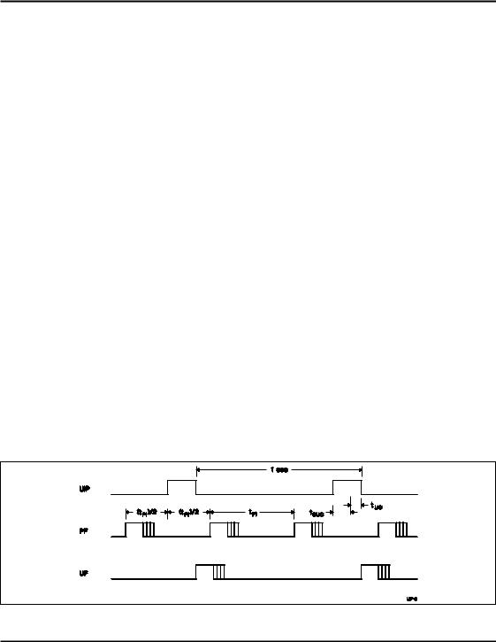
Update Period
The update period for the bq3285E/L is one second. The bq3285E/L updates the contents of the clock and calen-
dar locations during the update cycle at the end of each update period (see Figure 2). The alarm flag bit may also be set during the update cycle.
The bq3285E/L copies the local register updates into the user buffer accessed by the host processor. When a 1 is written to the update transfer inhibit bit (UTI) in register B, the user copy of the clock and calendar bytes remains unchanged, while the local copy of the same bytes continues to be updated every second.
The update-in-progress bit (UIP) in register A is set tBUC time before the beginning of an update cycle (see Figure 2). This bit is cleared and the update-complete flag (UF) is set at the end of the update cycle.
Figure 1. Address Map
Figure 2. Update Period Timing and UIP
Apr. 1999 D
4

bq3285E/L
Programming the RTC
The time-of-day, alarm, and calendar bytes can be written in either the BCD or binary format (see Table 2).
These steps may be followed to program the time, alarm, and calendar:
1.Modify the contents of register B:
a.Write a 1 to the UTI bit to prevent transfers between RTC bytes and user buffer.
b.Write the appropriate value to the data format (DF) bit to select BCD or binary format for all time, alarm, and calendar bytes.
c.Write the appropriate value to the hour format (HF) bit.
2.Write new values to all the time, alarm, and calendar locations.
3.Clear the UTI bit to allow update transfers.
On the next update cycle, the RTC updates all 10 bytes in the selected format.
Table 2. Time, Alarm, and Calendar Formats
|
|
|
Range |
|
|
|
|
|
|
|
|
|
|
|
|
Binary-Coded |
|
Address |
RTC Bytes |
Decimal |
Binary |
Decimal |
|
|
|
|
|
|
|
0 |
Seconds |
0–59 |
00H–3BH |
00H–59H |
|
|
|
|
|
|
|
1 |
Seconds alarm |
0–59 |
00H–3BH |
00H–59H |
|
|
|
|
|
|
|
2 |
Minutes |
0–59 |
00H–3BH |
00H–59H |
|
|
|
|
|
|
|
3 |
Minutes alarm |
0–59 |
00H–3BH |
00H–59H |
|
|
|
|
|
|
|
|
Hours, 12-hour format |
1–12 |
01H–OCH AM; |
01H–12H AM; |
|
4 |
81H–8CH PM |
81H–92H PM |
|||
|
|
||||
|
|
|
|
||
|
Hours, 24-hour format |
0–23 |
00H–17H |
00H–23H |
|
|
|
|
|
|
|
|
Hours alarm, 12-hour format |
1–12 |
01H–OCH AM; |
01H–12H AM; |
|
5 |
81H–8CH PM |
81H–92H PM |
|||
|
|
||||
|
|
|
|
||
|
Hours alarm, 24-hour format |
0–23 |
00H–17H |
00H–23H |
|
|
|
|
|
|
|
6 |
Day of week (1=Sunday) |
1–7 |
01H–07H |
01H–07H |
|
|
|
|
|
|
|
7 |
Day of month |
1–31 |
01H–1FH |
01H–31H |
|
|
|
|
|
|
|
8 |
Month |
1–12 |
01H–0CH |
01H–12H |
|
|
|
|
|
|
|
9 |
Year |
0–99 |
00H–63H |
00H–99H |
|
|
|
|
|
|
Apr. 1999 D
5

bq3285E/L
Square-Wave Output
The bq3285E/L divides the 32.768kHz oscillator frequency to produce the 1Hz update frequency for the clock and calendar. Thirteen taps from the frequency divider are fed to a 16:1 multiplexer circuit. The output of this mux is fed to the SQW output and periodic interrupt generation circuitry. The four least-significant bits of register A, RS0–RS3, select among the 13 taps (see Table 3). The square-wave output is enabled by writing a 1 to the square-wave enable bit (SQWE) in register B. A 32.768kHz output may be selected by setting OSC2–OSC0 in register A to 011 while SQWE = 1 and 32KE = 1.
Interrupts
The bq3285E/L allows three individually selected interrupt events to generate an interrupt request. These three interrupt events are:
■The periodic interrupt, programmable to occur once every 122μs to 500ms.
■The alarm interrupt, programmable to occur once per second to once per day, is active in battery-backup mode, providing a “wake-up” feature.
■The update-ended interrupt, which occurs at the end of each update cycle.
Each of the three interrupt events is enabled by an individual interrupt-enable bit in register B. When an event occurs, its event flag bit in register C is set. If the corresponding event enable bit is also set, then an interrupt request is generated. The interrupt request flag bit (INTF) of register C is set with every interrupt request. Reading register C clears all flag bits, including INTF, and makes INT high-impedance.
Two methods can be used to process bq3285E/L interrupt events:
■Enable interrupt events and use the interrupt request output to invoke an interrupt service routine.
■Do not enable the interrupts and use a polling routine to periodically check the status of the flag bits.
The individual interrupt sources are described in detail in the following sections.
Table 3. Square-Wave Frequency/Periodic Interrupt Rate
|
|
Register A Bits |
|
|
Square Wave |
Periodic Interrupt |
||||
OSC2 |
OSC1 |
OSC0 |
RS3 |
RS2 |
RS1 |
RS0 |
Frequency |
Units |
Period |
Units |
0 |
1 |
0 |
0 |
0 |
0 |
0 |
None |
|
None |
|
0 |
1 |
0 |
0 |
0 |
0 |
1 |
256 |
Hz |
3.90625 |
ms |
0 |
1 |
0 |
0 |
0 |
1 |
0 |
128 |
Hz |
7.8125 |
ms |
0 |
1 |
0 |
0 |
0 |
1 |
1 |
8.192 |
kHz |
122.070 |
μs |
0 |
1 |
0 |
0 |
1 |
0 |
0 |
4.096 |
kHz |
244.141 |
μs |
0 |
1 |
0 |
0 |
1 |
0 |
1 |
2.048 |
kHz |
488.281 |
μs |
0 |
1 |
0 |
0 |
1 |
1 |
0 |
1.024 |
kHz |
976.5625 |
μs |
0 |
1 |
0 |
0 |
1 |
1 |
1 |
512 |
Hz |
1.95315 |
ms |
0 |
1 |
0 |
1 |
0 |
0 |
0 |
256 |
Hz |
3.90625 |
ms |
0 |
1 |
0 |
1 |
0 |
0 |
1 |
128 |
Hz |
7.8125 |
ms |
0 |
1 |
0 |
1 |
0 |
1 |
0 |
64 |
Hz |
15.625 |
ms |
0 |
1 |
0 |
1 |
0 |
1 |
1 |
32 |
Hz |
31.25 |
ms |
0 |
1 |
0 |
1 |
1 |
0 |
0 |
16 |
Hz |
62.5 |
ms |
0 |
1 |
0 |
1 |
1 |
0 |
1 |
8 |
Hz |
125 |
ms |
0 |
1 |
0 |
1 |
1 |
1 |
0 |
4 |
Hz |
250 |
ms |
0 |
1 |
0 |
1 |
1 |
1 |
1 |
2 |
Hz |
500 |
ms |
0 |
1 |
1 |
X |
X |
X |
X |
32.768 |
kHz |
same as above defined |
|
|
by RS3–RS0 |
|||||||||
|
|
|
|
|
|
|
|
|
||
|
|
|
|
|
|
|
|
|
|
Apr. 1999 D |
|
|
|
|
|
|
|
|
|
|
|
6
bq3285E/L
Periodic Interrupt
The mux output used to drive the SQW output also drives the interrupt-generation circuitry. If the periodic interrupt event is enabled by writing a 1 to the periodic interrupt enable bit (PIE) in register C, an interrupt request is generated once every 122μs to 500ms. The period between interrupts is selected by the same bits in register A that select the square wave frequency (see Table 3). Setting OSC2–OSC0 in register A to 011 does not affect the periodic interrupt timing.
Alarm Interrupt
The alarm interrupt is active in battery-backup mode, providing a “wake-up” capability. During each update cycle, the RTC compares the hours, minutes, and seconds bytes with the three corresponding alarm bytes. If a match of all bytes is found, the alarm interrupt event flag bit, AF in register C, is set to 1. If the alarm event is enabled, an interrupt request is generated.
An alarm byte may be removed from the comparison by setting it to a “don’t care” state. An alarm byte is set to a “don’t care” state by writing a 1 to each of its two most-significant bits. A “don’t care” state may be used to select the frequency of alarm interrupt events as follows:
■If none of the three alarm bytes is “don’t care,” the frequency is once per day, when hours, minutes, and seconds match.
■If only the hour alarm byte is “don’t care,” the frequency is once per hour, when minutes and seconds match.
■If only the hour and minute alarm bytes are “don’t care,” the frequency is once per minute, when seconds match.
■If the hour, minute, and second alarm bytes are “don’t care,” the frequency is once per second.
Update Cycle Interrupt
The update cycle ended flag bit (UF) in register C is set to a 1 at the end of an update cycle. If the update interrupt enable bit (UIE) of register B is 1, and the update transfer inhibit bit (UTI) in register B is 0, then an interrupt request is generated at the end of each update cycle.
Accessing RTC bytes
The EXTRAM pin must be low to access the RTC registers. Time and calendar bytes read during an update cycle may be in error. Three methods to access the time and calendar bytes without ambiguity are:
■Enable the update interrupt event to generate interrupt requests at the end of the update cycle. The interrupt handler has a maximum of 999ms to access the clock bytes before the next update cycle begins (see Figure 3).
■Poll the update-in-progress bit (UIP) in register A. If UIP = 0, the polling routine has a minimum of tBUC time to access the clock bytes (see Figure 3).
■Use the periodic interrupt event to generate interrupt requests every tPI time, such that UIP = 1 always occurs between the periodic interrupts. The interrupt handler has a minimum of tPI/2 + tBUC time to access the clock bytes (see Figure 3).
Oscillator Control
When power is first applied to the bq3285E/L and VCC is above VPFD, the internal oscillator and frequency divider are turned on by writing a 010 pattern to bits 4 through 6 of register A. A pattern of 011 behaves as 010 but additionally transforms register C into a read/write register. This allows the 32.768kHz output on the square wave pin to be turned on. A pattern of 11X turns the oscillator on, but keeps the frequency divider disabled. Any other pattern to these bits keeps the oscillator off.
Figure 3. Update-Ended/Periodic Interrupt Relationship
Apr. 1999 D
7

bq3285E/L
Power-Down/Power-Up Cycle
The bq3285E and bq3285L power-up/power-down cycles are different. The bq3285L continuously monitors VCC for out-of- tolerance. During a power failure, when VCC falls below VPFD (2.53V typical), the bq3285L write-protects the clock and storage registers. The power source is switched to BC when VCC is less than VPFD and BC is greater than VPFD, or when VCC is less than VBC and VBC is less than VPFD. RTC operation and storage data are sustained by a valid backup energy source. When VCC is above VPFD, the power source is VCC. Writeprotection continues for tCSR time after VCC rises above VPFD.
The bq3285E continuously monitors VCC for out-of-tolerance. During a power failure, when VCC falls below VPFD (4.17V typical), the bq3285E write-protects the clock and storage registers. When VCC is below VBC (3V typical), the power source is switched to BC. RTC operation and storage data are sustained by a valid backup energy source. When VCC is above VBC, the power source is VCC. Write-protection continues for tCSR time after VCC rises above VPFD.
Control/Status Registers
The four control/status registers of the bq3285E/L are accessible regardless of the status of the update cycle (see Table 4).
Register A provides:
■ Status of the update cycle.
RS0–RS3 - Frequency Select
7 |
6 |
5 |
4 |
3 |
2 |
1 |
0 |
- |
- |
- |
- |
RS3 |
RS2 |
RS1 |
RS0 |
These bits select one of the 13 frequencies for the SQW output and the periodic interrupt rate, as shown in Table 3.
OS0–OS2 - Oscillator Control
7 |
6 |
5 |
4 |
3 |
2 |
1 |
0 |
- |
OS2 |
OS1 |
OS0 |
- |
- |
- |
- |
These three bits control the state of the oscillator and divider stages. A pattern of 010 enables RTC operation by turning on the oscillator and enabling the frequency divider. A pattern of 011 behaves as 010 but additionally transforms register C into a read/write register. This allows the 32.768kHz output on the square wave pin to be turned on. A pattern of 11X turns the oscillator on, but keeps the frequency divider disabled. When 010 is written, the RTC begins its first update after 500ms.
UIP - Update Cycle Status
Register A
Register A Bits
7 |
6 |
5 |
4 |
3 |
2 |
1 |
0 |
UIP |
OS2 |
OS1 |
OS0 |
RS3 |
RS2 |
RS1 |
RS0 |
Register A programs:
■The frequency of the square-wave and the periodic event rate.
■Oscillator operation.
7 |
6 |
5 |
4 |
3 |
2 |
1 |
0 |
UIP |
- |
- |
- |
- |
- |
- |
- |
This read-only bit is set prior to the update cycle. When UIP equals 1, an RTC update cycle may be in progress. UIP is cleared at the end of each update cycle. This bit is also cleared when the update transfer inhibit (UTI) bit in register B is 1.
Table 4. Control/Status Registers
|
Loc. |
|
|
|
|
|
|
|
|
|
Bit Name and State on Reset |
|
|
|
|
|
|
|||||||
|
|
|
7 (MSB) |
|
6 |
5 |
|
|
4 |
3 |
|
2 |
|
|
1 |
0 (LSB) |
||||||||
Reg. |
(Hex) |
Read |
Write |
|
|
|
|
|
|
|||||||||||||||
A |
0A |
Yes |
Yes1 |
UIP |
na |
OS2 |
|
na |
OS1 |
|
na |
OS0 |
|
na |
RS3 |
na |
RS2 |
|
na |
RS1 |
|
na |
RS0 |
na |
B |
0B |
Yes |
Yes |
UTI |
na |
PIE |
|
0 |
AIE |
|
0 |
UIE |
|
0 |
SQWE |
0 |
DF |
|
na |
HF |
|
na |
DSE |
na |
C |
0C |
Yes |
No2 |
INTF |
0 |
PF |
|
0 |
AF |
|
0 |
UF |
|
0 |
- |
0 |
32KE |
|
na |
- |
|
0 |
- |
0 |
D |
0D |
Yes |
No |
VRT |
na |
- |
|
0 |
- |
|
0 |
- |
|
0 |
- |
0 |
- |
|
0 |
- |
|
0 |
- |
0 |
Notes: na = not affected.
1.Except bit 7.
2.Read/write only when OSC2–OSC0 in register A is 011 (binary).
Apr. 1999 D
8

bq3285E/L
Register B
Register B Bits
7 |
6 |
5 |
4 |
3 |
2 |
1 |
0 |
UTI |
PIE |
AIE |
UIE |
SQWE |
DF |
HF |
DSE |
Register B enables:
■Update cycle transfer operation
■Square-wave output
■Interrupt events
■Daylight saving adjustment Register B selects:
■Clock and calendar data formats All bits of register B are read/write.
DSE - Daylight Saving Enable
7 |
6 |
5 |
4 |
3 |
2 |
1 |
0 |
- |
- |
- |
- |
- |
- |
- |
DSE |
This bit enables daylight-saving time adjustments when written to 1:
■On the last Sunday in October, the first time the bq3285E/L increments past 1:59:59 AM, the time falls back to 1:00:00 AM.
■On the first Sunday in April, the time springs forward from 2:00:00 AM to 3:00:00 AM.
HF - Hour Format
7 |
6 |
5 |
4 |
3 |
2 |
1 |
0 |
- |
- |
- |
- |
- |
- |
HF |
- |
This bit selects the time-of-day and alarm hour format:
1 = 24-hour format
0 = 12-hour format
DF - Data Format
7 |
6 |
5 |
4 |
3 |
2 |
1 |
0 |
- |
- |
- |
- |
- |
DF |
- |
- |
This bit selects the numeric format in which the time, alarm, and calendar bytes are represented:
1 = Binary
0 = BCD
Apr. 1999 D
SQWE - Square-Wave Enable
7 |
6 |
5 |
4 |
3 |
2 |
1 |
0 |
- |
- |
- |
- |
SQWE |
- |
- |
- |
This bit enables the square-wave output: 1 = Enabled
0 = Disabled and held low
UIE - Update Cycle Interrupt Enable
7 |
6 |
5 |
4 |
3 |
2 |
1 |
0 |
- |
- |
- |
UIE |
- |
- |
- |
- |
This bit enables an interrupt request due to an update ended interrupt event:
1 = Enabled
0 = Disabled
The UIE bit is automatically cleared when the UTI bit equals 1.
AIE - Alarm Interrupt Enable
7 |
6 |
5 |
4 |
3 |
2 |
1 |
0 |
- |
- |
AIE |
- |
- |
- |
- |
- |
This bit enables an interrupt request due to an alarm interrupt event:
1 = Enabled
0 = Disabled
PIE - Periodic Interrupt Enable
7 |
6 |
5 |
4 |
3 |
2 |
1 |
0 |
- |
PIE |
- |
- |
- |
- |
- |
- |
This bit enables an interrupt request due to a periodic interrupt event:
1 = Enabled
0 = Disabled
9
 Loading...